Note: Descriptions are shown in the official language in which they were submitted.
CA 02956948 2017-02-03
225675B
ELECTRONIC SELF-CALIBRATION FOR SENSOR CLEARANCE
This application is a division of Canadian Application Serial. No. 2,682,067
filed
October 9, 2009.
BACKGROUND
The present description relates generally to methods and systems for
calibration of a
sensor system, and more particularly to calibration of differential sensing
systems.
Various types of sensor systems have been used to measure the distance between
two
objects. One of such sensor systems includes a two-channel differential
sensing
system. In a two channel differential sensing system, various error sources
that affect
the two channels uniformly can be eliminated or reduced. Matching a response
of the
two channels is of utmost importance to be able to realize the benefits of the
differential measurement. Any mismatch in the response of the two channels
results
in significant error in a measurement. For example, the error in clearance
measurement results in inaccurate displacement between a shroud and a turbine
blade
of a turbine. It is therefore desired to dynamically and periodically check
and correct
the matching of the response of the two channels in the system. Variation in
electronic components due to temperature effects and long term drifts are two
reasons
for change in response of the channel.
Various techniques in circuit design have been utilized to reduce the
temperature
coefficient of circuits and to reduce the effect of the drifts. However, these
techniques
don't ensure measurement accuracy over a long period of time. A commonly used
technique is use of temperature compensated components in the sensor system.
Another commonly used technique is use of very low drift components. Both of
these
methods reduce the variation, but make no provision for detecting and
correcting
drifts and variations over time and temperature. Current clearance sensing
systems
rely heavily on frequent lab calibration to address this problem. For example,
for a
flight system that requires many years of service without human intervention,
calibration must be done in a transparent way and must not require the system
be
taken apart, or any human intervention.
1
CA 02956948 2017-02-03
225675B
BRIEF DESCRIPTION
In accordance with one exemplary embodiment of the present invention, a system
for
self-calibration of multiple channel clearance sensor system is provided. The
system
includes a sensor for measuring a clearance parameter between a stationary
object
and a rotating object. The system also includes an offset correction section
to
determine an offset error in the clearance parameter and a level shifter to
shift the
clearance parameter by the offset error. An amplifier is provided to amplify
the level
shifter output and an analog to digital converter is coupled to the amplifier
output to
provide a digital output. The system further includes a signal level analyzer
to
determine a channel gain signal based on a discrepancy voltage. The level
shifter in
the system is switchably coupled to the clearance parameter signal and a
reference
signal to process the discrepancy voltage
In accordance with another exemplary embodiment of the present invention, a
system
for self-calibration of a clearance sensor system is provided. As in the
earlier
embodiment, the system includes a sensor, an offset correction section, a
level shifter,
an amplifier and a signal level analyzer. However, in this embodiment the
clearance
parameter signal and a reference signal to process the discrepancy voltage are
coupled
together to the level shifter.
In accordance with one embodiment of the present invention, a method for
calibrating
a multiple channel sensor system is provided. The method includes measuring a
clearance parameter between a stationary object and a rotating object,
measuring an
offset error in the clearance parameter and shifting the clearance parameter
to
compensate for the offset error. The method further includes measuring a
discrepancy
in the clearance parameter and controlling gain values of the channel based on
the
measured discrepancy.
In accordance with yet another embodiment of the present invention a system
for self-
calibration of a sensor system is provided. The system includes a sensor and a
calibration section coupled to the sensor. The calibration section consists of
a level
shifter, a gain stage and a signal level analyzer for processing calibration
curves. The
2
CA 02956948 2017-02-03
225675B
calibration section further includes a reference section providing a common
mode
reference.
DRAWINGS
These and other features, aspects, and advantages of the present invention
will
become better understood when the following detailed description is read with
reference to the accompanying drawings in which like characters represent like
parts
throughout the drawings, wherein;
FIG. 1 is a diagrammatical representation of a rotating machine having a
sensor
system, in accordance with an embodiment of the present invention;
FIG. 2 is a diagrammatical representation of a sensor system of FIG. 1, in
accordance
with an embodiment of the present invention;
FIG. 3 is a diagrammatical representation of an exemplary system for clearance
measurement in accordance with an embodiment of the present invention;
FIG. 4a is a schematic illustration of an exemplary absolute calibration
section, in
accordance with an embodiment of the present invention;
FIG. 4b is a schematic illustration of another exemplary absolute calibration
section,
in accordance with an embodiment of the present invention;
FIG. 5 is a schematic illustration of an exemplary relative calibration
section, in
accordance with another embodiment of the present invention;
FIG. 6 is a schematic illustration of an offset calibration section in
accordance with
an embodiment of the present invention; and
FIG. 7 is a flowchart illustrating steps of calibration of the sensor system.
DETAILED DESCRIPTION
As discussed in detail herein, embodiments of the invention include a system
and
method for self-calibration of clearance measurement.
3
CA 02956948 2017-02-03
225675B
FIG. 1 is a perspective view of an exemplary rotating machine, such as an
aircraft
engine turbine 10, wherein aspects of the present technique can be
incorporated. It
should be noted here, however, that the present technique can be used in any
other
rotating machine such as but not limited to steam turbine and gas turbine. The
turbine
includes a rotor 12 mounted on a shaft 14. A plurality of turbine blades 16,
are affixed
to the rotor 12. In operation, the blades 16 are subject to a fluid 18 or
steam at a high
temperature and pressure, which does work on the blades 16 and causes them to
rotate
about an axis 20. The blades 16 rotate within a stationary housing or shroud
22 that
is positioned approximately radially and circumferentially around the blades.
There
is a relatively small clearance between the blades 16 and the shroud 22 to
prevent
excessive leakage of the working fluid between the blades 16 and the shroud
22. In
the ideal no loss system, there should be no clearance, so all the fluid will
work on
blades 16 only. However, that configuration will make movement of blades
impossible due to the resistance between the blades 16 and the shroud 22 or to
prevent
rubs between the rotor blades 16 and the shroud 22. A zero clearance system is
also
impractical because of vibrations.
In accordance with one embodiment, one or more clearance sensors 24 are
disposed
within and circumferentially around the stationary shroud 22. In the
illustrated
embodiment, the clearance sensors 24 include capacitive probes. Capacitive
probe
sensors provide variable capacitance as a representative of the clearance. In
certain
embodiments, the clearance sensors 24 may include microwave based sensors,
optical
sensors, or eddy current sensors. As will be appreciated by those skilled in
the art,
microwave sensors or optical sensors emit a radio signal or a light signal
respectively
on the target and measure characteristics of the reflection that is based on
the
clearance. These characteristics may include the amplitude of the reflected
signal, a
time delay or phase difference between an excitation and a reflected signal.
Similarly,
eddy current sensors induce eddy currents in the target. The interaction of
the
magnetic fields produced by eddy currents and the sensor currents depends on
clearance. The eddy current sensor then provides a voltage output
representative of
the clearance. The target in one embodiment is a turbine blade.
4
CA 02956948 2017-02-03
225675B
One advantage of using capacitive sensors is it provides sub mills resolution.
Each
of the sensors 24 is configured to generate a signal indicative of a radial
and/or an
axial position of the blades 16 with respect to the shroud 22 at their
respective
circumferential locations. The sensor signals 26 are transmitted to a
clearance
measurement system 28 for measuring the clearance. Further, the clearance
measurement through the clearance measurement system 28 is used for
controlling
the clearance between the shroud 22 and the turbine blades 16 via a clearance
control
system 30. The sensor signals 26 can be communicated to the clearance
measurement
system 28 via a signal wire or wirelessly via a wireless transmitter or
transceiver (not
shown). The communication can be unidirectional from the sensors to the
clearance
measurement system or bidirectional between the sensors and the measurement
system.
Fig. 2 illustrates an exemplary configuration of a clearance measurement
system 28
of Fig. 1. The system 28 in this embodiment comprises first and second sensors
40,
42 configured to generate first and second measurement signals representative
of first
and second capacitance between the shroud 22 and the rotor blades 16 of steam
turbine of Fig. 1.
In this example, the clearance 32 between the shroud and the rotor blades of
the
turbine is calculated by ratiometric techniques from first and second signal
of first
and second sensor 40, 42. A bidirectional coupler 44 and a phase detector 46
are
coupled to the first sensor 40 for measuring the capacitance through the first
sensor
40. Similarly, a bidirectional coupler 48 and a phase detector 50 are coupled
to the
second sensor 42 for measuring the capacitance through the second sensor 42. A
signal generator 52 is coupled to the first and second sensors 40 and 42 for
exciting
the first and second sensors. Further, first and second amplifiers 54, 56 are
coupled
to the signal generator 52 to amplify input signals generated from the signal
generator
52. The amplifiers 54, 56 are optional depending upon the signal generation
capability and filtering can also be used to condition the signal generator
output. In
one embodiment, a capacitor (not shown) can be deployed in series with each
sensors
40, 42 and signal generator 52 and the phase detectors 46, 52 can be coupled
on either
side of the capacitor.
CA 02956948 2017-02-03
225675B
According to one embodiment, the signal generator 52 at an excitation
frequency
excites first and second sensors 40, 42 via the first and second excitation
signals 62,
64. A first and second reflected signal 58, 60 corresponding to the first and
second
excited signal 62, 64 will originate from the first and second sensors 40, 42.
The
capacitance through the first sensor 40 is measured by measuring a phase
difference
between the excitation signal 62 and the corresponding reflected signal 58 by
the
bidirectional coupler 44 and the phase detector 46. The phase detector 46 is
configured to detect a first reflected signal 58 based upon the excitation
frequency to
generate first measurement signal 66. Similarly, measuring a phase difference
between the excitation signal 64 and the corresponding reflected signal 60 by
the
bidirectional coupler 48 and the phase detector 50 generates the second
measurement
signal 68 representative of the capacitance through the second sensor 42. The
first
and second measurement signals 66 and 68 are then transmitted to a calibration
section 70 for calculation of the clearance based upon a function of the first
and
second measurement signals 66 and 68. In one embodiment the function is a
ratio
between first and second measurement signals. As described herein, the sensor
system 28 in this example employs two sensors 40, 42 for capacitive
measurements
between the rotor blades 22 and the shroud 16. However, other configurations
of the
sensor system having more sensors are within the scope of the system.
The capacitance between two objects that are approximately in a parallel plate
configuration is given by following equation:
C = ,Eõ ¨A (1);
where, C is the capacitance, A is the overlap surface area of the object, d is
the
distance between the two objects, sõ is permittivity of free space and sr is
the
permittivity of a medium between the two objects. From equation (1), it can be
seen
that the capacitance between two objects depends on the distance between two
objects. Thus, by calculating the capacitance between the shroud and the rotor
blades,
the distance between the shroud and the rotor blades is thereby calculated.
6
CA 02956948 2017-02-03
225675B
In one embodiment, the processing circuitry 70 includes a filter (not shown)
and a
combiner (not shown). The output signals 66, 68 from the phase detectors 46,
50 may
include a noise component due to crosstalk between the first sensor 40 and the
second
sensor 42. Thus, a filter can be used to filter signal noise generated by the
crosstalk
between the sensors. The combiner combines the output signals from the phase
detectors to determine a ratiometric capacitance between the shroud and the
rotor
blades. The ratiometric capacitance provides a substantially accurate error-
minimized capacitance measurement between the shroud and the rotor blades.
FIG. 3 is a diagrammatical illustration of an exemplary system 80 for
clearance
measurement for a rotating machine. In the illustrated embodiment, sensors 82
measure and generate signals representing clearance parameter. As explained
earlier
the sensors may be capacitive probe sensors, microwave based sensors, optical
sensors, or eddy current sensors. In one embodiment and offset correction
section is
used to determine the offset error in the clearance parameter signals 84. In
one
example, a DC level finder determines offset error in the clearance
measurement
signal and level shifters 86 are used in the system to correct the offset
errors in the
clearance measurement signals. The system further comprises signal level
analyzers
88 to determine the difference between the channel sensor outputs. In one
embodiment, a reference scheme 90 is used for matching the channel gains. The
reference scheme 90 may include an automatic gain controller and it can be an
absolute scheme or a relative scheme. It should be noted that the offset
correction
section and the signal level analyzer can be implemented in an analog domain
or by
appropriate programming of a digital processor, or a combination of analog and
digital circuitry such as amplifiers, microprocessors, analog-to-digital
converters and
digital-to-analog converters. One embodiment is a two channel sensor system
however multiple channel processing is also within the scope of the invention.
In one
multiple channel embodiment, the channels can be referenced to each other
while in
another embodiment one of the channels is selected as a reference channel. For
example, certain applications such as radial and axial clearance, that uses
multiple
sensors in the processing.
7
CA 02956948 2017-02-03
225675B
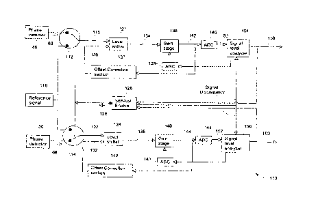
FIG. 4a is one representation 110 of an exemplary calibration circuitry in
FIG. 2. This
figure shows signal conditioning gain with absolute gain correlation for a two-
channel
system. As explained herein, in a two channel differential sensing system,
tight
matching of the response of the two channels results in higher performance.
The
reference to channel herein refers to the sensor(s) and its corresponding
elements that
are used to determine clearance such as shown in FIG. 1. Any mismatch in the
response of the two channels will reduce the common-mode error rejection
ability of
the system. The calibration section ensures the errors between first and
second
clearance measurement signals 66 and 68 are common-mode and ensures that any
error signals that are common to both channels continue to have an identical
effect on
the output of both channels after passing through the signal conditioning. In
the
illustrated example, first switch 112 and second switch 114 are coupled to the
first
phase detector 46 and the second phase detector 50 respectively. The first and
second
clearance measurement signals 66, 68 from the first and second phase detector
46, 50
are the first inputs to the first and second switches 112 and 114. In this
example the
first and second switches 112, 114 are single pole double through (SPDT)
switches.
As will be appreciated by those skilled in the art SPDT switch can have two
positions
thereby allowing the processing section to connect to either the phase
detector signals
66, 68 or a reference signal 116. In another embodiment, the switches 112, 114
are
radio frequency controlled switches that operate via multiple radio frequency
signals
in a desired range. In another embodiment the switch may be a MEMS switch.
Other
switching mechanisms can be employed which are known to those in the art.
A common reference signal 116 is a switched input to the first and the second
switches. Applying the common reference signal 116 to the calibration section
110
via the first and the second switch 112, 114 allows for establishing a common
reference point that ensures that differential error between the channels is
minimized.
An output signal 118 of the first switch 112 is an input to a first level
shifter 120.
Similarly, an output signal 122 of the second switch 114 is an input to a
second level
shifter 124. A self-test enable 126 generates an enable signal 128 for the
first and
second switches 112, 114 to control the switching for the reference signal
116. In
one embodiment, if the enable signal 128 is 'high', the reference signal 116
is the first
8
CA 02956948 2017-02-03
225675B
input 118, 122 to the level shifters 120, 124. If the enable signal is 'low',
the output
signal of phase detector 46, 50 is the first input 118, 122 to the level
shifters 120, 124
respectively. In one embodiment, the self-test enable circuit 126 generates
the enable
signal 128 at a pre-determined switching interval or in response to a
calibration
request signal.
The level shifters 120, 124 shift the input signals 118, 122 by a level
provided by the
shift level input signals 130, 132. The shift level input signals 130 and 132
are
provided by offset correction circuitry 137 and 143 respectively. The output
signals
134, 136 of the level shifters 120, 124 are then transmitted to the gain
stages 138, 140
or the amplifiers. The amplifiers 138, 140 amplify the output signals 134, 136
from
the level shifters 120, 124. There may be automatic gain controller (AGC) 139,
141
coupled to each corresponding gain stage 138, 140 to maintain a referenced
amplification.
In one embodiment, the reference signal source 116 used is a temperature
compensated very low drift components source. Thus, a high accuracy reference
signals ensures that the gain of the amplifier is also well controlled. The
output
signals from the amplifier 142 and 144 are then input to analog-to-digital
converters
146, 148 that converts signals 142, 144 to digital calibrated signals 150,
152. The
analog-to-digital converter 146, 148 outputs the calibrated voltages into
signal level
analyzers 154, 156. Voltage signal outputs or channel gain signals 158, 160
from the
signal level analyzers 154, 156 are used to generate calibration curves for
processing
that can be done in real-time or for post processing. The channel gain signals
158,
160 from the signal level analyzers 154, 156 are also coupled to the self-test
enable
126. The self-test enable 126 then controls the switching of the signals
between the
reference signal 116 and the phase detector output signals 66, 68. When the
reference
signal 116 is the input to the level shifters 120, 124, discrepancy in the
voltage signals
158 and 160 obtained from first and second signal level analyzers 154 and 156
respectively is measured. Accordingly, the gain one or both of the gain stages
138,
141 is then adjusted to match the respective discrepancy in the voltage
signals 158
and 160. In one embodiment, the adjustment takes place in the analog domain
through the use of controllable components such as variable gain amplifiers.
In
9
CA 02956948 2017-02-03
225675B
another embodiment, the discrepancy signal is digitized and a digital gain
correction
is calculated. The gain correction signal is used to correct the gain of the
two channels
in the digital domain.
It should be understood that while the explanation is directed to a two
channel system,
the system is not restricted to two channels and other embodiments have
multiple
channel processing capabilities. For example, a three-channel embodiment would
have three sensors and accompanying processing elements as detailed herein
with the
reference signal switched between the three channels. In one further
embodiment,
certain elements can be shared and the various sensors can be switched as
appropriate.
In one embodiment of the present invention, the DC level component in the
phase
detector signal and gain values of amplifiers are detected and tracked
periodically by
using on board references and algorithms to track these values. The
information is
then sent to a processing unit. The processing unit calculates correction
factors for
each channel and also tracks the history of corrections. The processor applies
the
corrections to the data i.e. corrections to the gain of the amplifiers or
corrections to
the shift level signal of the level shifter. The corrections are done to have
high degree
of matching between the characteristics of the two channels. If after the
corrections,
a trend is detected by the processor that the gain or offset is drifting at a
high rate,
health assessments of the sensor, and electronics are made. Based on the
assessment,
the processor may trigger an alert indicating that a higher than expected
error or
deterioration is detected and a service request for the clearance sensor
system is
dispatched. In a particular embodiment, the gain is adjusted via a digital
multiplier.
Fig. 4b is another representation of an exemplary calibration circuitry 170 of
FIG. 2.
In this embodiment, the phase detector output signals 66, 68 and the reference
signal
117 are both inputs to the level shifters 120, 124. In other words, the first
and second
switches 112 and 114 and the self-test enable circuit 126 of earlier
embodiment are
omitted in this embodiment. A summer 172 is used to combine the phase detector
output signal 66 and the reference signal 117 as appropriate to provide
correlation.
Similarly, a summer 174 adds the phase detector output signal 68 and the
reference
signal 117. In this embodiment, a frequency of the reference signal 117 and a
CA 02956948 2017-02-03
225675B
frequency of the output signals 66, 68 of the phase detectors 46, 50 are
different and
offset adequately so there is no effect by having the reference signal 117
combined
with the phase detector output signals 66, 68. In one embodiment, the
frequency of
the reference signal 117 is about 500 kHz and the frequency of the output
signals 66,
68 of the phase detectors 46, 50 are about 100 kHz. It should be noted,
however, that
other values of frequencies can be used for these signals. This configuration
enables
simultaneous connection of the phase detector signal and the reference signal,
and
therefore ensures continuous input of the phase detectors 46, 50 outputs to
the level
shifters 120, 124. The reference signal processing can be performed at various
time
intervals or as otherwise established by design criteria.
FIG. 5 illustrates another exemplary configuration 180 of the calibration
circuitry in
FIG. 2. This example shows the signal conditioning gain with relative gain
correlation between channels such that there is a relative reference signal
processing.
In this embodiment, output 66 of the first phase detector 46 is an input to
second
switch 114. Similarly, output 68 of the second phase detector 50 is an input
to the
first switch 112. In one embodiment, when the self-test enable signal 128 is
switched,
input signal 118, 122 to the first and second level shifters 120, 124 is the
output signal
66 of first phase detector 46. In another embodiment, when the self-test
enable signal
128 is switched, input signal 118, 122 to the first and second level shifters
120, 124
is the output signal 68 of second phase detector 50. This configuration avoids
use of
separate reference signal 116, 117 of FIG. 4a or FIG. 4b for the purpose of
calibration.
As noted herein, while described in a two channel implementation, multiple
channels
are a further embodiment and the reference processing can be implemented among
the channels.
FIG. 6 is a schematic representation 190 of an offset correction circuitry of
FIG. 4a,
FIG. 4b, and FIG. 5 wherein the elements for only one channel are depicted.
Similar
functionality would be used for the other channel and there could be a common
reference link such as coupling the inputs to the DC level finder 204. The
reference
signal is used to calculate an error signal between the actual DC level of the
signal
and the desired DC level. Using a common reference link in the DC level finder
ensures that errors in the reference contribute equally to both channels, and
therefore
11
CA 02956948 2017-02-03
225675B
maintains a high degree of matching between the two channels. According to one
embodiment this performs electronic offset processing and comprises a level
shifter
192 configured to shift the level of a first input signal 194 based on a
second input
signal 196 of the level shifter 192. In one embodiment, the first input signal
194 is
the first measurement signal 66 (FIG. 2) from first sensor 40 of FIG. 2. In
another
embodiment, the second input signal 196 of the level shifter 192 is a shift
level signal
or an offset signal. The offset correction circuitry 190 further comprises a
gain stage
198 or an amplifier to amplify the output signal 200 of the level shifter 192.
The gain
stage output 202 is then used as measurement signal for calculation of
clearance. The
gain stage output signal 202 is also fed back to a DC level finder 204. The DC
level
finder 204 determines the DC component in the gain stage output signal. The
error
signal output of the DC level finder 204 is transmitted to a level shifter
correction
circuitry 206. The level shifter correction circuitry 206 then determines the
offset by
which the first input signal 194 of the level shifter 192 need to be shifted.
Dynamic
adjustment of the level shifter 192 ensures that large offsets do not saturate
the
amplifier stage 198. In one embodiment, similar offset correction circuitry is
used
for the second channel of FIG. 4a, FIG. 4b, and FIG. 5. The offset correction
circuitry
190 is shown in a structural presentation however certain functionality may be
implemented via software processing.
FIG. 7 is a flowchart 220 illustrating steps of calibration of the multiple
channel
sensor system according to one embodiment. In step 221, the clearance
parameter
between the stationary object and the rotating object is measured using sensor
channels. In step 222, an offset error in the clearance parameter is measured
using an
offset correction circuitry. In step 224, both the sensor channels are
provided with a
reference signal, whether a common reference signal such as shown in FIG. 4a,
FIG.
4b or via the relative processing of FIG. 5. As described earlier, the common
reference signal source will have temperature compensated very low drift
components to control the gain properly. In one embodiment, in step 224, the
output
responses of the channels are measured and compared against each other. In
other
words, discrepancy between the channel output signals is measured. In step
226, the
gain values of the amplifiers in the channels are controlled based on the
measured
12
CA 02956948 2017-02-03
225675B
discrepancy between two output signals and in step 228, the discrepancy or the
error
is tracked periodically. In one embodiment, a threshold value of the error is
set in the
memory of a processor. If the error is larger than the threshold value or
larger than
an expected error trend, then the processor triggers an alert indicating a
maintenance
request for the clearance sensor system in step 230. As explained herein, in
one of
the absolute calibration examples, a self-test enable circuit controls the
input to the
channels between the reference signal and the actual sensor output signal. The
alert
provides a mechanism to determine the health of the system and there are
various
alerting mechanisms such as audio, visual or both as well as notification
schemes that
can dispatch emails, text messages, or dial phone numbers.
As will be appreciated by those of ordinary skill in the art, the foregoing
method or
part of the method and the process steps may be implemented by suitable
computer
program code on a processor-based system, such as a general-purpose or special-
purpose computer. The computer program code, as will be appreciated by those
of
ordinary skill in the art, may be stored or adapted for storage on one or more
tangible,
machine readable media, such as on memory chips, local or remote hard disks,
optical
disks (that is, CD's or DVD's), or other media, which may be accessed by a
processor-
based system to execute the stored code. Note that the tangible media may
comprise
paper or another suitable medium upon which the instructions are printed. For
instance, the instructions can be electronically captured via optical scanning
of the
paper or other medium, then compiled, interpreted or otherwise processed in a
suitable manner if necessary, and then stored in a computer memory.
While only certain features of the invention have been illustrated and
described
herein, many modifications and changes will occur to those skilled in the art.
It is,
therefore, to be understood that the appended claims are intended to cover all
such
modifications and changes as fall within the scope of the invention.
13