Note: Descriptions are shown in the official language in which they were submitted.
CA 2958964 2017-02-23
GAS DISCHARGE TUBES AND METHODS AND ELECTRICAL SYSTEMS
INCLUDING SAME
FIELD OF THE INVENTION
[0001] The present invention relates to circuit protection devices and, more
particularly, to overvoltage protection devices and methods.
BACKGROUND
[0002] Frequently, excessive voltage or current is applied across service
lines that
deliver power to residences and commercial and institutional facilities. Such
excess voltage
or current spikes (transient overvoltages and surge currents) may result from
lightning strikes,
for example. The above events may be of particular concern in
telecommunications
distribution centers, hospitals and other facilities where equipment damage
caused by
overvoltages and/or current surges and resulting down time may be very costly.
SUMMARY
[0003] According to embodiments of the invention, a gas discharge tube
includes a
housing defining a chamber, first and second terminal electrodes mounted on
the housing, a
plurality of inner electrodes located in the chamber, and a gas contained in
the chamber. The
inner electrodes are serially disposed in the chamber in spaced apart relation
to define a series
of spark gaps from the first terminal electrode to the second terminal
electrode. The chamber
is hermetically sealed.
[0004] In some embodiments, the plurality of electrodes includes at least
three inner
electrodes defining at least four inner spark gaps.
[0005] In some embodiments, the housing includes an insulator and a cover
forming
the housing and defining the chamber, and the insulator is formed of an
electrically insulating
material. The cover may be electrically conductive.
[0006] According to some embodiments, at least some of the inner electrodes
are
curved plates.
[0007] In some embodiments, the inner electrodes are captured in the chamber
to
permit limited displacement between the housing and the inner electrodes.
CA 2958964 2017-02-23
[0008] The gas discharge tube may further include a trigger device that is
contained in
the housing and that is electrically conductively coupled to either one of the
first terminal
electrode or the second terminal electrode and to ones of the plurality of
inner electrodes.
[0009] In some embodiments, the trigger device is disposed in the chamber.
[00010] According to some embodiments, the trigger device includes: a
substrate
formed of an electrically insulating material; and a plurality of resistor
links mounted on the
substrate, wherein the resistor links are configured to conduct current from
the inner
electrodes.
[00011] In some embodiments, the trigger device includes holes defined in the
substrate to permit electrical connection between the resistor links and the
inner electrodes.
[00012] According to some embodiments, each of the resistor links includes a
resistor
layer bonded to the substrate, the resistor layer being formed of an
electrically resistive
material. The electrically resistive material may include graphite in an
adhesive carrier. In
some embodiments, each of the resistor links further includes a terminal
interface layer
between the resistor layer thereof and the inner electrode associated with the
resistor link, and
the terminal interface layer is formed of metal.
[00013] According to some embodiments, each of the resistor links has a
resistance
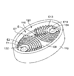
value in the range of from about 3 to 500 ohm.
[00014] The trigger device may include integral locator features that secure
the inner
electrodes in position in the chamber.
[00015] The housing may include integral locator features that secure the
inner
electrodes in position in the chamber.
[00016] In some embodiments, the housing includes a partition wall that
divides the
chamber into fluidly connected first and second subchambers, the first
terminal electrode is
disposed in the first subchamber, the second terminal electrode is disposed in
the second
subchamber; and some of the inner electrodes are disposed in the first
subchamber and some
of the inner electrodes are disposed in the second subchamber.
[00017] In some embodiments, the inner electrodes are concentric,
cylindrically-
shaped plates, and the second terminal includes an annular wall concentric
with and
circumferentially surrounding the inner electrodes.
[00018] In some embodiments, the trigger device includes first and second
substrates
each formed of an electrically insulating material, at least one resistor link
mounted on the
first substrate, and at least one resistor link mounted on the second
substrate. The resistor
2
CA 2958964 2017-02-23
links are configured to conduct current from the inner electrodes. In some
embodiments, the
second substrate is stacked on the first substrate.
[00019] In some embodiments, the gas contained in the chamber comprises
helium.
In some embodiments, the helium gas is present in the chamber in an amount of
at least 50%
by volume of the total volume of gas in the chamber. In some embodiments, the
gas
contained in the chamber comprises a mixture of helium and at least one other
gas.
[00020] According to method embodiments of the invention, a method includes:
electrically conductively coupling a first terminal electrode to a phase line
of a power system
and a second terminal electrode to a neutral line of a power system; providing
a plurality of
inner electrodes that are arranged between first terminal electrode and the
second terminal
electrode and that are spaced apart from one another; and electrically
conductively coupling a
plurality of resistors between respective ones of the plurality of inner
electrodes and the
second terminal electrode.
[00021] In some embodiments, the providing the plurality of inner electrodes
comprises arranging the plurality of inner electrodes to define a plurality of
spark gaps
between the first electrode and a first one of the plurality of the inner
electrodes, between
ones of the plurality of inner electrodes and between a second one of the
plurality of inner
electrodes and the second terminal.
[00022] According to some embodiments, responsive to a system operating
voltage
being present on the phase line, no current flows between the first terminal
electrode and the
second terminal, and responsive to an overvoltage condition being present on
the phase line, a
current flows from the first terminal electrode to the second terminal
electrode. In some
embodiments, the current that flows from the first terminal electrode to the
second terminal
electrode flows across the plurality of spark gaps.
[00023] The method may further include providing a housing that defines a
chamber,
wherein the first terminal electrode and the second terminal electrode are
mounted on the
housing, wherein the plurality of inner electrodes are located in the chamber,
and wherein the
plurality of resistors are located in the chamber.
[00024] According to embodiments of the technology, an overvoltage protection
circuit includes at least one housing defining at least one hermetically
sealed chamber, and a
series of spaced apart electrodes defining a series of spark gaps therebetween
located in the at
least one chamber. A gas is contained in the at least one chamber. The gas
contained in the
at least one chamber includes helium.
3
[0024a] In another aspect, there is provided a gas discharge tube comprising:
a
housing defining a chamber; first and second terminal electrodes mounted on
the housing; a
plurality of inner electrodes located in the chamber; a gas contained in the
chamber; wherein
the inner electrodes are serially disposed in the chamber in spaced apart
relation to define a
series of spark gaps from the first terminal electrode to the second terminal
electrode;
wherein the chamber is hermetically sealed; and wherein: the gas discharge
tube includes a
trigger device that is contained in the housing and that is electrically
conductively coupled to
either one of the first terminal electrode or the second terminal electrode
and to ones of the
plurality of inner electrodes; the gas discharge tube includes the trigger
device is disposed in
the hermetically sealed chamber with the inner electrodes and in fluid
communication with
the gas; and the trigger device includes a plurality of resistor links
configured to conduct
current from the inner electrodes.
10024b] In another aspect, there is provided a gas discharge tube comprising:
a
housing defining a chamber; first and second terminal electrodes mounted on
the housing; a
plurality of inner electrodes located in the chamber; and a gas contained in
the chamber;
wherein the inner electrodes are serially disposed in the chamber in spaced
apart relation to
define a series of spark gaps from the first terminal electrode to the second
terminal
electrode; wherein the chamber is hermetically sealed; wherein the gas
discharge tube further
comprises a trigger device that is contained in the housing and that is
electrically
conductively coupled to either one of the first terminal electrode or the
second terminal
electrode and to ones of the plurality of inner electrodes; wherein the
trigger device includes
a plurality of resistor links; wherein the resistor links are configured to
conduct current from
the inner electrodes; and wherein the inner electrodes are captured in the
chamber such that
limited displacement is permitted between the housing and the inner
electrodes.
100240 In yet another aspect, there is provided a gas discharge tube
comprising: a
housing defining a chamber; first and second terminal electrodes mounted on
the housing; a
plurality of inner electrodes located in the chamber; a gas contained in the
chamber; wherein
the inner electrodes are serially disposed in the chamber in spaced apart
relation to define a
series of spark gaps from the first terminal electrode to the second terminal
electrode;
wherein the chamber is hermetically sealed; and wherein: the inner electrodes
are concentric,
cylindrically-shaped plates; and the second terminal includes an annular wall
concentric with
and circumferentially surrounding the inner electrodes.
[0024d] In still another aspect, there is provided a gas discharge tube
comprising: a
housing defining a chamber; first and second terminal electrodes mounted on
the housing; a
4
Date Recue/Date Received 2022-05-14
plurality of inner electrodes located in the chamber; a gas contained in the
chamber; wherein
the inner electrodes are serially disposed in the chamber in spaced apart
relation to define a
series of spark gaps from the first terminal electrode to the second terminal
electrode; and
wherein the chamber is hermetically sealed; wherein: the gas discharge tube
includes a
trigger device that is contained in the housing and that is electrically
conductively coupled to
either one of the first terminal electrode or the second terminal electrode
and to ones of the
plurality of inner electrodes; the trigger device includes: a substrate formed
of an electrically
insulating material; and a plurality of resistor links mounted on the
substrate; wherein the
resistor links are configured to conduct current from the inner electrodes;
each of the resistor
links includes a resistor layer bonded to the substrate, the resistor layer
being formed of an
electrically resistive material; and the resistor links each have a different
length.
[00025] It is noted that aspects of the invention described with respect to
one
embodiment, may be incorporated in a different embodiment although not
specifically
described relative thereto. That is, all embodiments and/or features of any
embodiment can
be combined in any way and/or combination. These and other objects and/or
aspects of the
present invention are explained in detail in the specification set forth
below.
Brief Description of the Drawin2s
[00026] The accompanying figures are included to provide a further
understanding of
the present invention, and are incorporated in and constitute a part of this
specification. The
drawings illustrate some embodiments of the present invention and, together
with the
description, serve to explain principles of the present invention.
[00027] FIG. 1 is a bottom perspective view of a gas discharge tube (GDT)
according
to some embodiments of the invention.
[00028] FIG. 2 is a top perspective view of the GDT of FIG. 1.
[00029] FIG. 3 is an exploded, top perspective view of the GDT of FIG. 1.
[00030] FIG. 4 is an exploded, bottom perspective view of the GDT of FIG. 1.
[00031] FIG. 5 is a fragmentary top perspective view of the GDT of FIG. 1.
[00032] FIG. 6 is cross-sectional view of the GDT of FIG. 1 taken along the
line 6-6
of FIG. 2.
[00033] FIG. 7 is cross-sectional view of the GDT of FIG. 1 taken along the
line 7-7
of FIG. 6.
[00034] FIG. 8 is a fragmentary top plan view of the GDT of FIG. 1.
4a
Date Recue/Date Received 2022-05-14
[00035] FIG. 9 is a bottom plan view of a trigger device forming a part of the
GDT of
FIG. 1.
[00036] FIG. 10 is a schematic view of an electrical assembly including the
GDT of
FIG. 1.
[00037] FIGS. 11A and 11B are electrical schematic circuits representing two
different embodiments corresponding to the GDT of FIG. 1.
[00038] FIG. 12 is a bottom perspective view of a gas discharge tube (GDT)
according to further embodiments of the invention.
[00039] FIG. 13 is an exploded, top perspective view of the GDT of FIG. 12.
[00040] FIG. 14 is an exploded, bottom perspective view of the GDT of FIG. 12.
[00041] FIG. 15 is cross-sectional view of the GDT of FIG. 12 taken along the
line
15-15 of FIG. 12.
4b
Date Recue/Date Received 2022-05-14
" CA 2958964 2017-02-23
[00042] FIG. 16 is a fragmentary top perspective view of the GDT of FIG. 12.
[00043] FIG. 17 is a fragmentary top plan view of the GDT of FIG. 12.
[00044] FIG. 18 is a fragmentary top plan view of the GDT of FIG. 12.
[00045] FIG. 19 is a top perspective view of a gas discharge tube (GDT)
according to
further embodiments of the invention.
[00046] FIG. 20 is an exploded, top perspective view of the GDT of FIG. 19.
[00047] FIG. 21 is a fragmentary top perspective view of the GDT of FIG. 19.
[00048] FIG. 22 is cross-sectional view of the GDT of FIG. 12 taken along the
line
22-22 of FIG. 19.
[00049] FIG. 23 is a fragmentary top plan view of the GDT of FIG. 19.
[00050] FIG. 24 is a bottom perspective view of a trigger device forming a
part of the
GDT of FIG. 19.
[00051] FIG. 25 is a top perspective view of a gas discharge tube (GDT)
according to
further embodiments of the invention.
[00052] FIG. 26 is an exploded, top perspective view of the GDT of FIG. 25.
[00053] FIG. 27 is an exploded, top perspective view of the GDT of FIG. 25.
[00054] FIG. 28 is cross-sectional view of the GDT of FIG. 25 taken along the
line
28-28 of FIG. 25.
[00055] FIG. 29 is a bottom perspective view of a trigger device forming a
part of the
GDT of FIG. 25.
[00056] FIG. 30 is a top perspective view of a gas discharge tube (GDT)
according to
further embodiments of the invention.
[00057] FIG. 31 is an exploded, bottom perspective view of the GDT of FIG. 30.
[00058] FIG. 32 is an exploded, top perspective view of the GDT of FIG. 30.
[00059] FIG. 33 is cross-sectional view of the GDT of FIG. 30 taken along the
line
33-33 of FIG. 30.
[00060] FIG. 34 is a fragmentary top plan view of the GDT of FIG. 30.
[00061] FIG. 35 is a bottom plan view of a trigger device forming a part of
the GDT
of FIG. 30.
[00062] FIG. 36 is an enlarged, fragmentary view of the GDT of FIG. 30
including
an alternative trigger device.
[00063] FIG. 37 is an enlarged, fragmentary view of the GDT of FIG. 30
including a
further alternative trigger device.
CA 2958964 2017-02-23
[00064] FIGS. 38 and 39 are exploded, perspective views of a gas discharge
tube
(GDT) according to further embodiments of the invention.
[00065] FIGS. 40-43 are perspective views illustrating a method of assembling
the
GDT of FIG. 38.
[00066] FIG. 44 is a cross-sectional view of the GDT of FIG. 38 taken along
the line
44-44 of FIG. 38.
Detailed Description of Embodiments of the Invention
[00067] The present invention now will be described more fully hereinafter
with
reference to the accompanying drawings, in which illustrative embodiments of
the invention
are shown. In the drawings, the relative sizes of regions or features may be
exaggerated for
clarity. This invention may, however, be embodied in many different forms and
should not
be construed as limited to the embodiments set forth herein; rather, these
embodiments are
provided so that this disclosure will be thorough and complete, and will fully
convey the
scope of the invention to those skilled in the art.
[00068] It will be understood that when an element is referred to as being
"coupled"
or "connected" to another element, it can be directly coupled or connected to
the other
element or intervening elements may also be present. In contrast, when an
element is
referred to as being "directly coupled" or "directly connected" to another
element, there are
no intervening elements present. Like numbers refer to like elements
throughout.
[00069] In addition, spatially relative terms, such as "under", "below",
"lower",
"over", "upper" and the like, may be used herein for ease of description to
describe one
element or feature's relationship to another element(s) or feature(s) as
illustrated in the
figures. It will be understood that the spatially relative terms are intended
to encompass
different orientations of the device in use or operation in addition to the
orientation depicted
in the figures. For example, if the device in the figures is turned over,
elements described as
"under" or "beneath" other elements or features would then be oriented "over"
the other
elements or features. Thus, the exemplary term "under" can encompass both an
orientation of
over and under. The device may be otherwise oriented (rotated 90 degrees or at
other
orientations) and the spatially relative descriptors used herein interpreted
accordingly.
[00070] Well-known functions or constructions may not be described in detail
for
brevity and/or clarity.
[00071] As used herein the expression "and/or" includes any and all
combinations of
one or more of the associated listed items.
6
= CA 2958964 2017-02-23
[00072] The terminology used herein is for the purpose of describing
particular
embodiments only and is not intended to be limiting of the invention. As used
herein, the
singular forms "a", "an" and "the" are intended to include the plural forms as
well, unless the
context clearly indicates otherwise. It will be further understood that the
terms "comprises"
and/or "comprising," when used in this specification, specify the presence of
stated features,
integers, steps, operations, elements, and/or components, but do not preclude
the presence or
addition of one or more other features, integers, steps, operations, elements,
components,
and/or groups thereof.
[00073] Unless otherwise defined, all terms (including technical and
scientific terms)
used herein have the same meaning as commonly understood by one of ordinary
skill in the
art to which this invention belongs. It will be further understood that terms,
such as those
defined in commonly used dictionaries, should be interpreted as having a
meaning that is
consistent with their meaning in the context of the relevant art and will not
be interpreted in
an idealized or overly formal sense unless expressly so defined herein.
[00074] As used herein, a "hermetic seal" is a seal that prevents the passage,
escape
or intrusion of air or other gas through the seal (i.e., airtight).
"Hermetically sealed" means
that the described void or structure (e.g., chamber) is sealed to prevent the
passage, escape or
intrusion of air or other gas into or out of the void or structure.
[00075] As used herein, "monolithic" means an object that is a single, unitary
piece
formed or composed of a material without joints or seams.
[00076] With reference to FIGS. 1-11, a modular, multi-cell gas discharge tube
(GDT) 100 according to embodiments of the invention is shown therein. The GDT
100
includes an insulator 110, a cover 130, a first terminal electrode 132, a
second terminal
electrode 134, a set E of inner electrodes E1-E14, an insulator 136, seals
135, 138, bonding
layers 137, 139, a trigger device 150, and a selected gas M (FIG. 6).
[00077] The insulator 110 and the cover 130 collectively form an enclosure or
housing 102 defining an enclosed GDT chamber 104 (FIG. 6). The terminal
electrodes 132,
134, the inner electrodes E1-E14, the insulator plate 136, the trigger device
150, and the gas
M are contained in the chamber 104. The housing 102 has a central axis A-A
(FIG. 1), a first
lateral axis B-B, and a second lateral axis C-C (FIG. 6). As discussed
hereinbelow, the
sixteen electrodes 132, 134, El-E14 define a plurality of gaps G (fifteen gaps
G) and a
plurality of cells C (fifteen cells C) between the electrodes 132, 134, E1-E14
(FIG. 6). The
electrodes 132, 134 E1-E14 and the gaps G and cells C are serially distributed
in spaced
apart relation along the axis B-B.
7
r
= CA 2958964 2017-02-23
[00078] The insulator 110 may be generally cup-shaped. The insulator 110
includes
an end or bottom wall 112 and an annular, elliptical, upstanding side wall 114
collectively
defining a cavity 120 and a top opening 122 communicating with the cavity 120.
Electrode
through holes or openings 124 extend through the bottom wall 112. Integral
locator features
or tabs 116 project upwardly from the bottom wall 112. The insulator 110, the
cavity 120
and the chamber 104 are elliptically shaped in cross-section perpendicular to
the axis A-A.
[00079] The insulator 110 may be formed of any suitable electrically
insulating
material. According to some embodiments, the insulator 110 is formed of a
material having a
melting temperature of at least 1000 degrees Celsius and, in some embodiments,
at least 1600
degrees Celsius. In some embodiments, the insulator 110 is formed of a
ceramic. In some
embodiments, the insulator 110 includes or is formed of alumina ceramic
(A1203) and, in
some embodiments, at least about 90% A1203. In some embodiments, the insulator
110 is
monolithic.
[00080] The electrodes 132, 134 each include a head 132A, 134A disposed in the
cavity 120 and a contact post 132B, 134B extending through a respective
opening 124 and
projecting outwardly from the insulator 110. A bonding layer 137 is interposed
between each
post 132B, 134B and the inner surface of its opening 124. The posts 132B, 134B
are bonded
to the insulator 110 by the bonding layers 137 continuously about the full
peripheries of the
openings 124. The bonding layers 137 along with the seals 138 hermetically
seal the
openings 124. In some embodiments, the bonding layers 137 are metallization,
solder or
metal-based layers. Suitable metal-based materials for forming the bonding
layers 137 may
include nickel-plated Ma-Mo metallization. Suitable materials for the seals
138 may include
silver-copper alloy.
[00081] The electrodes 132, 134 may be formed of any suitable material.
According
to some embodiments, the electrodes 132, 134 are formed of metal and, in some
embodiments, are formed of molybdenum or Kovar. According to some embodiments,
each
of the electrodes 132, 134 is unitary and, in some embodiments, monolithic.
[00082] As discussed above, the inner electrodes E1-E14 are serially
positioned and
distributed in the cavity 120 along the axis B-B. The electrodes E1-E14 are
positioned such
that each electrode E1-E14 is physically spaced apart from the immediately
adjacent other
inner electrode(s) E1-E14, 132, 134. The lower edge of each electrode E1-E14
is captured in
slots defined between associated ones of the locator tabs 116 to thereby limit
lateral
displacement of the electrode E1-E14 relative to the housing 102. Each
electrode E1-E14 is
8
CA 2958964 2017-02-23
also captured between the bottom wall 112 and the trigger device 150 to
thereby limit axial
displacement (along axis A-A) of the electrode E1-E14 relative to the housing
102.
[00083] In this manner, each electrode E1-E14 is positively positioned and
retained in
position relative to the housing 102 and the other electrodes E1-E14, 132,
134. In some
embodiments, the electrodes E1-E14 are secured in this manner without the use
of additional
bonding or fasteners applied to the electrodes El-E14. The electrodes El-E14
may be semi-
fixed or loosely captured between the locator features 116, the bottom wall
112 and the
triggering device 150. The electrodes E1-E14 may be capable of floating up and
down to a
limited degree within the housing 102.
[00084] The electrodes E1-E14 are each arcuate, bent or curved plates. More
particularly, each electrode E1-E14 has an arcuate, or curvilinear cross-
secitonal shape or
profile in the plane defined by the lateral axes B-B and C-C, and is straight,
flat or linear in
planes parallel to the plane defined by the axes A-A and C-C. The opposing
surfaces of the
electrodes E1-E14 extend substantially parallel to one another. This
configuration permits a
greater gap length within a housing 102 of a given width and for the
electrodes to have
similar lengths.
[00085] The electrodes El -E14 may be formed of any suitable material.
According
to some embodiments, the electrodes E1-E14 are formed of metal and, in some
embodiments,
are formed of molybdenum, copper, tungsten or steel. According to some
embodiments, each
of the electrodes E1-E14 is unitary and, in some embodiments, monolithic.
[00086] According to some embodiments, each of the electrodes E1-E14 has a
thickness T1 (FIG. 6) in the range of from about 0.3 to 2 mm and, in some
embodiments, in
the range of from about 0.5 to 1 mm. According to some embodiments, each
electrode El-
E14 has a height Hi (FIG. 7) in the range of from about Ito 20 mm and, in some
embodiments, in the range of from 3 to 10 mm. According to some embodiments,
the length
of each electrode El -E14 is in the range of from about 10 to 50 mm.
[00087] The insulator 136 may be shaped as a flat plate or otherwise
configured. The
insulator 136 may be formed of any suitable electrically insulating material.
According to
some embodiments, the insulator 136 is formed of a material having a melting
point of at
least 1000 degrees Celsius and, in some embodiments, at least 1600 degrees
Celsius. In some
embodiments, the insulator 136 is formed of a ceramic. In some embodiments,
the insulator
136 includes or is formed of alumina ceramic (A1203) and, in some embodiments,
at least
about 90% A1203. In some embodiments, the insulator 136 is monolithic.
9
CA 2958964 2017-02-23
[00088] The cover plate 130 may be shaped as a flat plate or otherwise
configured.
The cover plate 130 may be formed of any suitable material. According to some
embodiments, the cover plate 130 is formed of metal and, in some embodiments,
is formed of
copper or Kovar. According to some embodiments, the cover plate 130 is unitary
and, in
some embodiments, monolithic.
[00089] An annular bonding layer 139 is interposed between an annular top edge
surface 118 of the insulator 110 and the lower surface of the cover 130. The
seal 135 is
interposed between the bonding layer 139 and the cover 130. The cover 130 is
bonded to the
surface 118 by the bonding layer 139. According to some embodiments, the cover
130 is
bonded to the surface 118 by the bonding layer 139 continuously about the full
periphery of
the opening 122 so that the opening 122 is hermetically sealed by the cover
130 and the
bonding layer 139 and the seal 135. The bonding layer 139 may be formed of the
same
material as described above for the bonding layer 137. The seal layer 135 may
be formed of
the same material as described above for the seals 138.
[00090] The trigger device 150 (FIGS. 3, 4 and 7-9) includes a substrate 152,
a
plurality of resistor links R1-R14 (FIG. 8), and a conductor link 162. The
resistor links R1-
R14 and the conductor link 162 constitute a trigger circuit 151.
[00091] The substrate 152 includes a body 154 and an integral annular flange
156.
Recesses 158 are defined in the top side 154A of the body 154 and communicate
with
through holes 159 that extend to the bottom side 154B of the body 154. A
channel 157 is
also defined in the top side 154A.
[00092] The substrate 152 may be formed of any suitable electrically
insulating
material. According to some embodiments, the substrate 152 is formed of a
material having a
melting temperature of at least 1000 degrees Celsius and, in some embodiments,
at least 1600
degrees Celsius. In some embodiments, the substrate 152 is formed of a
ceramic. In some
embodiments, the substrate 152 includes or is formed of alumina ceramic
(A1203) and, in
some embodiments, at least about 90% A1203. In some embodiments, the substrate
152 is
monolithic.
[00093] With reference to FIGS. 7-9, the connecting layer 162 is bonded to the
top
surface of the substrate 152 in the channel 157. Each resistor link R1-R14
includes a resistor
layer 164 and a terminal interface layer 160. Each resistor link R1-R14 is
terminated on one
end by the connecting layer 162 and by its terminal interface layer 160 on its
opposing end.
The terminal interface layers 160 are thereby electrically connected to the
connecting layer
through the resistor layers 164. The terminal interface layers 160 are bonded
to the top
CA 2958964 2017-02-23
surface of the substrate 152 in respective ones of the recesses 158. The
terminal interface
layers 160 extend to and may extend into the through holes 159.
[00094] The connecting layer 162 may be formed of any suitable material.
According
to some embodiments, the connecting layer 162 is formed of metal and, in some
embodiments, is formed of metal in an adhesive carrier. In some embodiments,
the carrier is
a silicate-based adhesive carrier such as a sodium silicate or potassium
silicate adhesive.
According to some embodiments, the connecting layer 162 has a thickness in the
range of
from about 50 to 1000 micrometers.
[00095] The terminal interface layers 160 may be formed of any suitable
material.
According to some embodiments, the terminal interface layers 160 are formed of
metal and,
in some embodiments, are formed of metal in an adhesive carrier. In some
embodiments, the
carrier is a silicate-based adhesive carrier such as a sodium silicate or
potassium silicate
adhesive. According to some embodiments, each of the terminal interface layers
160 has a
thickness in the range of from about 50 to 1000 micrometers.
[00096] The resistor layers 164 may be formed of any suitable electrically
resistive
material. According to some embodiments, the resistor layers 164 are formed of
graphite-
based compound. According to some embodiments, the resistor layers 164 are
formed of a
compound including graphite in an adhesive carrier. In some embodiments, the
carrier is a
silicate-based adhesive carrier such as a sodium silicate or potassium
silicate adhesive.
[00097] According to some embodiments, the resistor layers 164 are formed of a
material having a specific electrical resistance in the range of from about 1
micro-ohm-meter
to 1 ohm-meter.
[00098] According to some embodiments, each of the resistor links R1-R14 has
an
electrical resistance in the range of from about 3 to 500 ohms.
[00099] According to some embodiments, each of the resistor layers 164 has a
thickness in the range of from about 1 to 150 micrometers.
[000100] The gas M may be any suitable gas, and may be a single gas or a
mixture of
two or more (e.g., 2, 3, 4, 5. or more) gases. According to some embodiments,
the gas M
includes at least one inert gas. In some embodiments, the gas M includes at
least one gas
selected from argon, neon, helium, hydrogen, and/or nitrogen. According to
some
embodiments, the gas M is or includes helium. In some embodiments, the gas M
may be air
and/or a mixture of gases present in air.
[000101] According to some embodiments, the gas M may comprise a single gas in
any suitable amount, such as, for example, in any suitable amount in a mixture
with at least
11
= CA 2958964 2017-02-23
one other gas. In some embodiments, the gas M may comprise a single gas in an
amount of
about 0.1%, 0.5%, 1%, 5%, 10%, 15%, 20%, 25%, 30%, 35%, 40%, 45%, 50%, 55%,
60%,
65%, 70%, 75%, 80%, 85%, 90%, 95%, 98%, or 99% by volume of the total volume
of gas
present in the GDT chamber 104, or any range therein. In some embodiments, the
gas M
may comprise a single gas in an amount of less than 50% (e.g., less than 40%,
30%, 20%,
10%, 5%, or 1%) by volume of the total volume of gas present in the GDT
chamber 104. In
some embodiments, the gas M may comprise a single gas in an amount of more
than 50%
(e.g., more than 60%, 70%, 80%, 90%, or 95%) by volume of the total volume of
gas present
in the GDT chamber 104. In some embodiments, the gas M may comprise a single
gas in an
amount in a range of about 0.5% to about 15%, about 1% to about 50%, or about
50% to
about 99% by volume of the total volume of gas present in the GDT chamber 104.
In some
embodiments, the gas M comprises at least one gas present in an amount of at
least 50% by
volume of the total volume of gas present in the GDT chamber 104. According to
some
embodiments, the gas M comprises helium in an amount of at least 50% by volume
of the
total volume of gas present in the GDT chamber 104. According to some
embodiments, the
gas M comprises at least one gas present in an amount of about 90% or more by
volume of
the total volume of gas present in the GDT chamber 104, and, in some
embodiments, in an
amount of about 100% by volume of the total volume of gas present in the GDT
chamber
104.
[000102] According to some embodiments, the gas M may comprise a mixture of a
first gas and a second gas (e.g., an inert gas) different from the first gas
with the first gas
present in an amount of less than 50% by volume of the total volume of gas
present in the
GDT chamber 104 and the second gas present in an amount of at least 50% by
volume of the
total volume of gas present in the GDT chamber 104. In some embodiments, the
first gas is
present in an amount in a range of about 5% to about 20% by volume of the
total volume of
gas present in the GDT chamber 104 and the second gas is present in an amount
of about
50% to about 90% by volume of the total volume of gas present in the GDT
chamber 104. In
some embodiments, the first gas is present in an amount of about 10% by volume
of the total
volume of gas present in the GDT chamber 104 and the second gas is present in
an amount of
about 90% by volume of the total volume of gas present in the GDT chamber 104.
In some
embodiments, the second gas is helium, which may be present in the proportions
described
above for the second gas. In some embodiments, the first gas (which may be
present in the
proportions described above for the first gas) is selected from the group
consisting of argon,
12
-
CA 2958964 2017-02-23
neon, hydrogen, and/or nitrogen, and the second gas is helium (which may be
present in the
proportions described above for the second gas).
[000103] The GDT 100 may be assembled as follows. The terminal electrodes 132
and 134 are inserted through the openings 159. The bonding layers 137 are
heated to bond
the terminals 132, 134 to the insulator 110 in the openings 124. The seals 138
are installed or
formed about the posts 132B, 134B to secure the electrodes 132, 134 in place
and
hermetically seal the openings 159. According to some embodiments, the seals
138 are metal
solder or brazings, which may be formed of silver-copper alloy, for example.
[000104] The inner electrodes E1-E14 are installed in the cavity 120. More
particularly, the electrodes E1-E14 are each installed in a respective set of
slots between the
locator features 116 as shown in FIG. 6.
[000105] The trigger device 150 is placed over the inner electrodes E1-E14 so
that
the bottom side 154B rests on the top edges 142A (FIG. 7) of the inner
electrodes E1-E14.
The trigger device 150 is aligned such that the through holes 159 are each
aligned with a
respective one of top edges 142A of the electrodes E1-E14, 134, and the
interface layers 160
therein are located on or closely adjacent said respective top edges 142A.
[000106] The insulator plate 136 and the cover 130 are then placed over the
trigger
device 150. The cover 130 is bonded to the top face 118 of the insulator 110
to form the
housing 102 and gas-tight sealed chamber 104. According to some embodiments,
the cover
130 is sealingly secured to the insulator 110 by brazing or heating the cover
130 and thereby
melt-bonding the bonding layer 139 to the cover 130. The bonding layer 139 may
be sprayed
onto or otherwise applied to the insulator 110.
[000107] In some embodiments, the components of the GDT 100 are disposed in an
assembly chamber during the steps of placing the cover 130 on the insulator
110 and securing
the cover 130 to the insulator 110 to enclose and seal the chamber 104. The
assembly
chamber is filled with the gas M at a prescribed pressure and temperature. As
a result, the
gas M is thereafter captured and contained in the chamber 104 of the assembled
GDT 100 at
a prescribed pressure and temperature. The prescribed pressure and temperature
are selected
such that the gas M is present at a desired operational pressure when the GDT
100 is installed
and in use at a prescribed service temperature.
[000108] In some embodiments, the pressure of the gas M in the chamber 104 of
the
assembled GDT 100 is in the range of from about 50 to 1000 mbar at 20 degrees
Celsius.
[000109] According to some embodiments, the relative dimensions of the
insulator
110, the electrodes E1-E14, the trigger device 150, the insulator plate 136,
and the cover 130
13
CA 2958964 2017-02-23
=
are selected such that the electrodes E1-E14 are loosely captured between the
substrate 152
and the insulator bottom wall 112 to permit the electrodes E1-E14 to slide up
and down a
small distance. In some embodiments, the permitted vertical float distance is
in the range of
from about 0.05 to 0.5 mm. In other embodiments, the substrate 152 and the
bottom wall 112
fit snuggly against or apply a compressive load to the electrodes E1-E14.
[000110] The electrodes 132, E1-E14, 134 define a plurality of gaps G and a
plurality
of cells C between each pair of electrodes 132, E1-E14, 134. According to some
embodiments, the minimum width W1 (FIG. 6) of each gap G (i.e., the smallest
gap distance
between the two electrode surfaces forming the cell C) is in the range of from
about 0.2 to 1.5
mm.
[000111] The through holes 159 associated with the resistor links R1-R14 are
positioned over the top edges 142A, 134C of the electrodes E1-E14 and 134,
respectively.
As a result, the terminal layer 160 of each resistor link R1-R14 is positioned
on or closely
adjacent the corresponding top edge 142A, 134C through the corresponding
through hole
159.
[000112] In use, the resistor links R1-R14 are electrically coupled to the
electrodes
E1-E14, 134 through their respective terminal layers 160. Because the
electrodes E1-E14
are floating or not fully fixed in the housing 102 and the terminal electrode
134 is spaced
from the trigger device 150, it may not be possible to ensure tight contact
between the resistor
links R1-R14 and the electrodes E1-E14, 134. As a result, a small gap J (FIG.
7) may be
present between each resistor link R1-R14 and its electrode E1-E14, 134.
According to
some embodiments, each gap J has a width in the range of from about 0 to 0.5
mm. During
a surge event, this gap J may cause sparking between the resistor link R1-R14
and the
electrode E1-E14, 134. If the sparking is applied to the resistor layer 164,
such sparking may
damage the resistor layer 164, which may in turn enlarge the gap and adversely
affect
performance of the GDT 100 (e.g., increase the required spark over voltage).
[000113] The terminal interface layers 160 can prevent or reduce such damage
to the
resistor links R1-R14 and thereby improve the performance and service life of
the GDT 100.
The material of the terminal interface layers 160 has an electrical
conductivity substantially
the same as the electrode and greater than that of the resistor layer 164 so
that the
aforementioned sparking is eliminated or reduced. Moreover, the material of
the terminal
interface layers 160 may be more resistant to degradation from etching than
the material of
the resistor layer 164.
14
= CA 2958964 2017-02-23
[000114] Advantageously, the plurality of spark gaps G are housed or enveloped
in
the same housing 102 and chamber 104. The plurality of cells C and spark gaps
G defined
between the electrodes 132, E1-E14, 134 are in fluid communication so that
they share the
same mass or volume of gas M. By providing multiple electrodes, cells and
spark gaps in
one common or shared chamber 104, the size and number of parts can be reduced.
As a
result, the size, cost and reliability of the GDT 100 can be reduced as
compared to a plurality
of individual GDTs connected in series.
[000115] Moreover, the trigger device 150 including the trigger circuit 151 is
housed
or enveloped in the same housing 102 and chamber 104 as the electrodes 132, E1-
E14, 134,
and is likewise in fluid communication with the same mass of gas M. As a
result, the size,
cost and reliability of the GDT 100 can be reduced as compared to a plurality
of individual
GDTs connected in series with an external trigger circuit.
[000116] The arcuate configurations of the electrodes E1-E14 can help to
ensure that,
in the case of a surge event, spark over occurs between the midsections of the
electrodes El-
E14, not at their edges.
[000117] The floating or semi-fixed mounting of the electrodes E1-E14 in the
housing 102 can facilitate ease of assembly.
[000118] The performance attributes of the GDT 100 can be determined by
selection
of the gas M, the pressure of the gas M in the chamber 104, the dimensions and
geometries of
the electrodes 132, E1-E14, 134, the geometry and dimensions of the housing
102, the sizes
of the gaps G, and/or the electrical resistances of the resistor links R1-R14.
[000119] In some embodiments and with reference to FIG. 10, an electrical
assembly
according to embodiments of the invention is shown therein. The electrical
assembly 5
incorporates the GDT 100. The GDT 100 is mounted in an enclosure 52 of a GDT
module 50
that is removeably and replaceably mounted on a base 60. The base 60 is in
turn mounted on
a support DR to mechanically and electrically connect the CDT 100 to an
electrical power
system. In some embodiments, the support DR is a DIN rail. The base 60
includes an
enclosure 62, a first electrical connector 64 to which a first electrical wire
WL (e.g., a line
wire) is secured and a second electrical connector 66 to which a second
electrical wire WN
(e.g., a neutral wire) is secured. The GDT module 50 includes a jumper 54
including
connectors 54A and 54B. The connector 54A is secured to the terminal electrode
132 and the
connector 54B is releasably interlocked with the base connector 64. The GDT
module 50
further includes a second jumper 56 including connectors 56A and 56B. The
connector 56A
is secured to the terminal electrode 134 and the connector 56B is releasably
interlocked with
CA 2958964 2017-02-23
the base connector 66. The jumper 56 may further include a thermal
disconnector
mechanism 56D.
[000120] Brief reference is now made to FIG. 11A, which is an electrical
schematic
circuit of a modular, multi-cell gas discharge tube 100 as illustrated in
FIGS. 1-9 according
to some embodiments of the present invention. As illustrated, in the
electrical schematic
context, the modular, multi-cell gas discharge tube 100 may include a
plurality of single cell
GDTs that are arranged serially between terminals 132 and 134. For example, a
first terminal
132 and the inner electrode El may function as a first single cell GDT1, the
inner electrode
El and the inner electrode E2 may function as a second single cell GDT2 that
is serially
connected to the first single cell GDT1 and so on.
[000121] Additionally, a trigger circuit 150 may include multiple resistors R1-
R14
that may be connected between respective ones of the inner electrodes E1-E14
and the
terminal 134. In some embodiments, the resistors R1-R14 include resistive
layers 164 and
are electrically conductively coupled to the connecting layer 162 and
interface layers 160. As
described above, the modular, multi-cell gas discharge tube 100 provides that
the interface
layers 160 are electrically conductively coupled to the inner electrodes EL-
E14.
[000122] In use and operation, the first terminal 132 may be connected to a
line or
phase voltage of a single or multi-phase power system and the second terminal
134 may be
connected to a neutral line of the single or multi-phase power system. The
total arcing
voltage of the modular, multi-cell gas discharge tube 100 generally
corresponds to the sum of
the arcing voltage of individual series connected single cell GDTs and thus
exceeds the peak
value of the system voltage. As such, when the modular, multi-cell gas
discharge tube 100 is
in conduction mode, the current flowing therethrough will be generally limited
to the current
corresponding to a surge event, such as lighting, and not from the system
source.
[000123] Under normal (i.e., non-conducting) conditions, since no current is
flowing
through GDT1, then no current is flowing through R1 and the voltage across
GDT1 is the
same as the line-neutral voltage at the second terminal 134. When an
overvoltage is applied
to the system, the overvoltage will be applied to the first terminal 132,
which is the top
electrode of GDT1. Since the lower electrode of GllTi, which is the inner
electrode El, is at
the same potential as the second terminal 134, GDT1 begins to conduct
electrical current and
the overvoltage is applied to the second GDT2, which includes inner electrodes
El and E2.
Also, once GDT1 begins to conduct, a small current will flow through resistor
Rl. In some
embodiments, the current may only flow through resistor RI until GDT2 begins
to conduct,
16
CA 2958964 2017-02-23
which may be a very short period of time. For example, current may only flow
through R1
for a time interval that is less than 1 microsecond.
[000124] As provided above, as soon as CDT] begins conducting, the overvoltage
is
applied to GDT2, which then begins to conduct. Once GDT2 begins to conduct,
the
overvoltage is applied to GDT3, which then begins to conduct. Similarly,
resistor R2 will
conduct a small amount of current once GDT2 begins conducting until GDT3
begins to
conduct. Once each of the series connected single cell GDTs conducts current,
the GDTs
stay in conduction mode until the overvoltage condition has ceased. Once the
overvoltage
condition ceases, the GDTs cease to conduct because the peak value of the
system voltage is
less than the total arcing voltage of the modular, multi-cell gas discharge
tube 100.
[0001251 The quantity of gaps in the modular, multi-cell gas discharge tube
100 may
vary depending on the operating voltage of the system. For example, for a 255V
application,
a modular, multi-cell gas discharge tube 100 may use between 14 and 21 total
gaps between
the terminal 132, the inner electrodes E1-E14 and the terminal 134. Some
embodiments
provide that the quantity of gaps may be less than 14 if the system voltage is
correspondingly
less than the examples provided herein and the quantity of gaps may be greater
than 21 if the
system voltage is correspondingly greater than the examples provided herein.
[000126] Additionally, some embodiments provide that the resistance values of
resistors R1-R14 may be in a range between about 3 Ohms to about 500 Ohms,
however,
such embodiments are non-limiting and the resistance values may be less than 3
Ohms and/or
greater than 500 Ohms. In some embodiments, the resistance values of resistors
R1-R14 may
all be the same, while in other embodiments the resistor values of resistors
R1-R14 may be
different from one another.
[000127] Brief reference is now made to FIG. 11B, which is an electrical
schematic
circuit of a modular, multi-cell gas discharge tube 100 as illustrated in
FIGS. 1-9 according
to some other embodiments of the present invention. Many elements as discussed
above
regarding FIG. 11A are substantially the same and thus duplicative discussion
thereof will be
omitted. As illustrated, an additional gap corresponding to GDT n may be added
in series
with the circuit of FIG. 11A. In this manner, instead of a single GDT (e.g.,
GDT1) beginning
to conduct to trigger the remaining GDTs into conduction, both GDT1 and GDT,,
must begin
conducting to trigger the conduction of the other GDTs. An advantage of having
both GDT1
and GDT, to begin conducting is that if either of GDT1 or GDT n short circuit
or begin to
degrade, a gap will still be present in the other GDT and the device may still
function. Such
17
= CA 2958964 2017-02-23
advantage may provide increased safety in operation, although response time
may be
increased.
[000128] Although the use and operation described above are provided in the
context
of the modular, multi-cell gas discharge tube 100, the description of the use
and operation
may be application to other embodiments described herein.
[000129] With reference to FIGS. 12-18, a modular, multi-cell GDT 200
according to
further embodiments of the invention is shown therein, The GDT 200 includes an
insulator
210, a cover 230, a first terminal electrode 232, a second terminal electrode
234, a set 2E of
inner electrodes 2E1-2E19, an insulator 236, seals 235, 238, bonding layers
237, 239, a
trigger device 250, and a selected gas M corresponding to the insulator 110,
the cover 130,
the first terminal electrode 132, the second terminal electrode 134, the inner
electrodes El-
E14, the insulator 136, the seals 135, 138, the bonding layers 137, 139, the
trigger device
150, and the selected gas M of the GDT 100, except as follows.
[000130] The electrodes 2E1-2E19, the trigger device 250, and the gas M are
all
contained in a hermetically sealed chamber 204 in a housing 202 formed by the
insulator 210
and the cover 230.
[000131] The insulator 210 includes an integral ceramic partition wall 215
that bisects
the cavity 220. The partition wall 215 divides the cavity 220 into subcavities
220A, 220B.
The substrate 252 of the trigger device 250 includes an integral ceramic rib
252A that is
received in a groove 215A defined in the top edge of the partition wall 215.
The insulator
210, the cavity 220 and the chamber 204 are cylindrically shaped.
[000132] The terminal electrodes 232, 234 are secured and sealed by the
bonding
layers 237 and the seals 238 in openings 224 on the same lateral end of the
cavity 220 and
opposite sides of the partition wall 215.
[000133] The arcuate inner electrodes 2E1-2E9 are secured in the subcavity
220A
and the arcuate inner electrodes 2E11-2E19 are secured in the subcavity 220B.
The inner
electrode 2E10 includes an integral first portion 244A in the subcavity 220A
and an integral
second portion 244B in the subcavity 220B. The electrode portions 244A, 244B
are
connected by an integral connecting portion 244C that extends through a slot
220C defined
between the sidewall 214 and an end of the partition wall 215. The electrodes
2E1-2E19 are
each arcuate, curved or bent plates that are curvilinear in lateral profile
and straight in axial
profile. The electrodes 2E1-2E19 are captured to be semi-fixed or floating by
the locator
features 216, the sidewall 214 and the partition wall 215.
18
CA 2958964 2017-02-23
[000134] The trigger device 250 includes a ceramic substrate 252, connecting
layers
262, and resistor links 2R2-2R19 corresponding to the ceramic substrate 152,
connecting
layers 162, and resistor links R1-R14 of the GDT 100. The terminal interface
layers 260 of
the first connecting layer 262 and the resistor links 2R2-2R19 are positioned
on or closely
adjacent the top edges of the electrodes 2E1-2E19 and 234, respectively,
through the through
holes 259 in the substrate 252.
[000135] The GDT 200 includes twenty spark gaps G and twenty cells C. In use,
spark over occurs sequentially from the electrode 232, through the electrodes
2E1-2E19 and
to the electrode 234. Spark over directly between the electrodes 2E1-2E9 in
the subcavity
220A and the electrodes 2E11-2E19 in the subcavity 220B is prevented by the
electrically
insulating partition wall 215 and rib 252A. The trigger device 250 operates in
the same
manner as described above with regard to the trigger device 150 to control the
firing
sequence and timing.
[000136] With reference to FIGS. 19-24, a modular, multi-cell GDT 300
according to
further embodiments of the invention is shown therein. The GDT 300 includes an
insulator
310, a cover 330, a first terminal electrode 332, a second terminal electrode
334, a set 3E of
inner electrodes 3E1-3E18, an insulator 336, seals 335, 338 bonding layers
337, 339, a
trigger device 350, and a selected gas M corresponding to the insulator 110,
the cover 130,
the first terminal electrode 132, the second terminal electrode 134, the inner
electrodes El-
E14, the insulator 136, the seals 135, 138, the bonding layers 137, 139, the
trigger device
150, and the selected gas M of the GDT 100, except as follows. The electrodes
3E1-3E18,
the trigger device 350, and the gas M are all contained in a hermetically
sealed chamber 304
in a housing 302 formed by the insulator 310 and the cover 330.
[000137] The insulator 310 includes integral ribs 317A defining locator slots
317B
therebetween. Opposed end openings 324 communicate with the cavity 320. The
insulator
310, the cavity 320 and the chamber 304 are rectangular in cross-section.
[000138] The terminal electrodes 332 and 334 are secured and sealed by the
bonding
layers 337 in the openings 324. The inner electrodes 3E1-3E18 are
substantially flat plates
with opposed planar faces. The electrodes 3E1-3E18 are seated in the slots
317B and thereby
semi-fixed or floatingly mounted in the chamber 304.
[000139] The trigger device 350 includes a ceramic substrate 352, connecting
layers
362, and resistor links 3R2-3R18 corresponding to the ceramic substrate 152,
connecting
layers 162, and resistor links R1-R14 of the GDT 100. The terminal interface
layers 360 of
the connecting layer 362 and the resistor links 3R2-3R18 are positioned on or
closely
19
CA 2958964 2017-02-23
adjacent the top edges of the electrodes 3E1-3E18 and 334, respectively,
through the through
holes 359 in the substrate 352.
[000140] The GDT 300 includes nineteen spark gaps G and nineteen cells C. In
use,
spark over occurs sequentially from the electrode 332, through the electrodes
3E1-3E18 and
to the electrode 334. The trigger device 350 operates in the same manner as
described above
with regard to the trigger device 150 to control the firing sequence and
timing.
[000141] With reference to FIGS. 25-29, a modular, multi-cell GDT 400
according to
further embodiments of the invention is shown therein. The GDT 400 includes an
insulator
410, a first terminal electrode 432, a second terminal electrode 434, a set 4E
of inner
electrodes 4E1-4E18, an insulator 436, bonding layers 437, seals 438, a
trigger device 450,
and a selected gas M corresponding to the insulator 110, the first terminal
electrode 132, the
second terminal electrode 134, the inner electrodes E1-E14, the insulator 136,
the bonding
layer 137, the seal 138, the trigger device 150, and the selected gas M of the
GDT 100,
except as follows.
[000142] The electrodes 4E1-4E18, the trigger device 450, and the gas M are
all
contained in a hermetically sealed chamber 404 in a housing 402 formed by the
insulator 410
and the electrodes 432, 434.
[000143] The insulator 410 is generally tubular and has opposed end openings
424
communicating with the cavity 420. The insulator 410, the cavity 420 and the
chamber 404
are rectangular in cross-section.
[000144] The insulator 436 is a plate having integral ribs 436A defining
locator slots
436B therebetween.
[000145] The trigger device 450 includes a ceramic substrate 452, connecting
layers
462, and resistor links 4R1-4R18 corresponding to the ceramic substrate 152,
connecting
layers 162, and resistor links R1-R18. The substrate 452 includes integral
ribs 453B defining
locator slots 453B therebetween.
[000146] The inner electrodes 4E1-4E18 are substantially flat plates with
opposed
planar faces.
[0001471 To assemble the GDT 400, the inner electrodes 4E1-4E18 are seated in
the
slots 436B of the insulator plate 436 on one side edge and are seated in the
slots 453B of the
trigger device 450 on the side edge to form a cassette or subassembly 403 as
shown in FIG.
27. The subsassembly 403 is inserted into the cavity 420 through the opening
424. The
terminal electrodes 432 and 434 are secured and sealed by the bonding layers
437 in the
openings 424. The inner electrodes 4E1-4E18 are semi-fixed or floatingly
secured in the
CA 2958964 2017-02-23
sealed chamber 404 by the locator ribs 436A, 453A and the top and bottom walls
of the
insulator 410.
[000148] The terminal interface layers 460 of the resistor links 4R1-4R18 are
positioned on or closely adjacent the top edges of the electrodes 4E1-4E18 and
434,
respectively, through the through holes 459 in the substrate 452.
[000149] The GDT 400 includes nineteen spark gaps G and nineteen cells C. In
use,
spark over occurs sequentially from the electrode 432, through the electrodes
4E1-4E18 and
to the electrode 434. The trigger device 450 operates in the same manner as
described above
with regard to the trigger device 150 to control the firing sequence and
timing.
[000150] With reference to FIGS. 30-35, a modular, multi-cell GDT 500
according to
further embodiments of the invention is shown therein. The GDT 500 includes an
insulator
510, a first terminal electrode 532, a second terminal electrode 534, a set 5E
of inner
electrodes 5E1-5E7, an insulator 536, a seal 538, bonding layers 537, 539, a
trigger device
550, and a selected gas M corresponding to the insulator 110, the first
terminal electrode 132,
the second terminal electrode 134, the inner electrodes E1-E14, the insulator
136, the seals
138, the bonding layers 137, 139, the trigger device 150, and the selected gas
M of the GDT
100, except as follows.
[000151] The electrodes 5E1-5E7, the trigger device 550, and the gas M are all
contained in a hermetically sealed chamber 504 in a housing formed by the
insulator 510 and
the electrode 534. The electrode 534 serves as a cover.
[000152] The insulator 510 includes an electrode opening 524 within which the
terminal electrode 532 is secured and hermetically sealed by a seal 538 and
the bonding layer
537. The insulator 510 includes a series of concentric, annular steps 519. The
steps 519
progressively increase in height in the direction from the terminal electrode
532 to the side
wall 514. The insulator 510, the cavity 520 and the chamber 504 are tubular or
cylindrically
shaped.
[000153] The terminal electrode 534 includes an end wall 534A and an annular
side
wall 534B. The side wall 534B is secured to the side wall 514 of the insulator
510 by the
bonding layer 539. The interface between the terminal electrode 534 and the
side wall 514 is
hermetically sealed by a seal 538 and the bonding layer 539.
[000154] The inner electrodes 5E1-5E7 are cylindrical and concentrically
mounted
on respective ones of the steps 519 in the chamber 504. The inner electrodes
5E1-5E7 are
radially spaced apart to define annular spark gaps G and cells C therebetween.
The
electrodes 5E1-5E7 are radially constrained by the steps 519 and axially
constrained by the
21
CA 2958964 2017-02-23
insulator bottom wall 512 and the trigger device 550 so that the electrodes
are semi-fixed or
floating in the chamber 504. The trigger device 550 is in turn constrained by
the insulator
plate 536 and the terminal electrode 534.
[0001551 The trigger device 550 includes a ceramic substrate 552 and resistor
links
5R1-5R7 corresponding to the ceramic substrate 152 and resistor links R1-R14
of the GDT
100. The terminal interface layers 560 of the resistor links 5R1-5R7 are
positioned in
recesses 558 and on or closely adjacent the top edges of the electrodes 5E1-
5E7 and 534,
respectively, through the through holes 559 in the substrate 552. Each
resistor link 5R1-5R7
includes a terminal contact 565 on its end opposite its terminal interface
layer 560. The
resistor links 5R1-5R7, respectively, are electrically connected to the
electrode 534 via their
respective terminal contacts 565. Small gaps may be present between the
electrode 534 and
some or all of the terminal contacts 565. According to some embodiments, the
terminal
contacts 565 are formed of a material as described above for the terminal
interface layers 160
in order to prevent sparking and degradation of the resistor layers 564 of the
resistor links
5R1-5R7 as discussed above with regard to the terminal interface layers 160
and the resistor
layers 164.
10001561 The GDT 500 includes eight spark gaps G and eight cells C. In use,
spark
over occurs sequentially from the electrode 532, through the electrodes 5E1-
5E7 and to the
electrode 534. The trigger device 550 operates in the same manner as described
above with
regard to the trigger device 150 to control the firing sequence and timing.
[000157] The terminal interface layers 560 may be masses or plugs of the
electrically
conductive material that substantially fill the holes 559 as shown and
described above with
regard to the terminal interface layers 160 and with reference to FIG. 7.
According to further
embodiments and as shown in FIG. 36, the terminal interface layers 560 may
take the form
of relatively thin layers 560' and the through holes 559 may remain open. The
terminal
interface layers 160, 260, 360, 460 may likewise be formed in this manner. A
gap J may be
present between each or some of the terminal interface layers 560' and their
respective
electrodes 5E1-5E7. According to some embodiments, each of the gaps J has a
width W5 of
less than about 0.5 mm.
[000158] According to further embodiments and with reference to FIG. 37, each
electrode 5E1-5E7 may include an integral contact protrusion or pin 557
projecting upwardly
from its top edge. The pin 557 is received in a respective through hole 559
and extends into
the associated recess 558. In this embodiment, each terminal interface layer
560 takes the
form of a terminal interface layer 560" that fills the space about the pin 557
in the recess 558.
22
CA 2958964 2017-02-23
Each terminal interface layer 560" is bonded to its corresponding resistor
layer 564 to the
ceramic 552 and to the pin 557 to effect electrical and mechanical connection
therebetween.
Thus, in this embodiment, the gaps between each terminal interface layer 560
and its
electrode may be eliminated. The terminal interface layers 160, 260, 360, 460
may likewise
be formed in this manner. This embodiment may be manufactured by installing
the pins 557
in the through holes 559, and then placing the material of the terminal
interface layers 560"
in the recesses 558 in molten or liquid form, after which the material
solidifies (e.g., by
drying or cooling) or heating (sintering) and bonds to the resistor layer,
ceramic and pin.
[000159] With reference to FIGS. 38-44, a modular multi-cell GDT 600 according
to
further embodiments of the invention is shown therein. While FIGS. 38 and 39
are exploded
views, the GDT 600 will outwardly appear substantially the same as the GDT 400
when
assembled. The GDT 600 includes an insulator 610, a first terminal electrode
632, a second
terminal electrode 634, a set 6E of inner electrodes 6E1-6E18 (FIG. 40),
bonding layers (not
labeled), seals (not labeled), and a selected gas (not labeled) corresponding
to the insulator
410, the first terminal electrode 432, the second terminal electrode 434, the
set 4E of inner
electrodes 4E1-4E18, the bonding layers 437, the seals 438, and the gas M of
the GDT 400,
except as discussed below. The GDT 600 further includes a multi-layered
trigger device 650
corresponding to the trigger device 450. The trigger device 650 performs the
same function
as the trigger device 450 in generally the same manner, but is differently
constructed in order
to provide improved and/or more consistent and reliable performance.
[000160] The inner electrodes 6E1-6E18 each include relatively short integral
locator
pins 653 (FIGS. 38 and 39) projecting from one side edge, and relatively long
integral
electrical contact pins 657 projecting from their opposed side edges. The
contact pins 657
have different lengths and are staggered in height along the electrode side
edges.
[000161] The trigger device 650 includes six discrete substrates 671, 672,
673, 674,
675, and 676. The substrates 671-676 may be formed in substantially the same
manner and
of the same material as the substrate 452.
10001621 Each of the substrates 671-676 includes three longitudinally
extending
grooves 677 extending along a lengthwise axis I-I (FIG. 44) from a proximal
end 677A to an
opposing distal end 677B (FIG. 38). The distal ends 677B each terminate
proximate, at or
closely adjacent a distal end 679 of the substrate 671-676. Laterally
extending through holes
678 extend fully through the thicknesses of the substrates 671-676. The
through holes 678
are axially staggered. One of the holes 678 terminates proximate the proximal
end 677A of
each groove 677.
23
CA 2958964 2017-02-23
[000163] The substrates 671 and 674 each include slots 617B corresponding to
slots
417B to receive and to secure the inner electrodes 6E1-6E18. The substrates
671, 674 also
include locator recesses 617C to receive the locator pins 653 to locate the
electrodes 6E1-
6E18 along the height axis. The substrate 671 includes axially distributed
recesses 671A
with a step 671B therebetween, The substrate 674 includes recesses 674A with a
step 674B
therebetween.
[000164] A respective resistor link 6R1-6R18 (FIGS. 39-42) is located in each
groove 677. Each resistor link 6R1-6R18 includes a resistor layer 664
corresponding to the
resistor layers 464, and terminal interface layers 660A, 660B corresponding to
the terminal
interface layers 460. The interface layers 660A are located at the through
holes 678. The
interface layers 660B are located at the distal ends 679. The trigger device
650 does not
include a conductive link corresponding to the connecting layer 462.
[000165] The second terminal electrode 634 (FIG. 44) includes an outer contact
section 634A, a trigger contact section 634B, and an electrode gap surface
634C.
[000166] The GDT 600 may be assembled in the same manner as the GDT 400,
except as follows. The substrates 671 and 674 are mounted on either side of
the set 6E of
electrodes as shown in FIG. 40. The edge portions of the electrodes 6E1-6E18
are received
in the slots 617B of the substrates 671, 674 and the electrodes 6E1-6E18 are
thereby captured
between the substrates 671, 674. The locator pins 653 are seated in the
locator recesses
617C. The contact pins 657 project through the holes 678. On one side, the
three distal most
contact pins 657 extend into the holes 678 the resistor links 6R16-6R18 of the
substrate 671
such that they make contact with or are positioned closely adjacent to the
interface layers
660A of the resistor links 6R16-6R18. On the other side, the distalmost
contact pins 657
extend into the holes 678 of the resistor links 6R13-6R15 of the substrate 674
such that they
make contact with or are positioned closely adjacent the interface layers 660A
of the resistor
links 6R13-6R15.
[000167] With reference to FIG. 41, the substrate 672 is mounted in the lower
recess
671A of the substrate 671 such that the middle three contact pins 657 on that
side extend
through the holes 678 in the substrate 672. These contact pins 657 make
contact with or are
located closely adjacent the interface layers 660A of the resistor links 6R10-
6R12. Similarly,
the substrate 675 is mounted in the lower recess 674A of the substrate 674
such that the
middle three contact pins 657 on that side extend through the holes 678 in the
substrate 675.
These contact pins 657 make contact with or are located closely adjacent to
the interface
layers 660A of the resistor links 6R7-6R9.
24
CA 2958964 2017-02-23
[000168] With reference FIG. 42, the substrate 673 is mounted over the
substrate 672
and in the upper recess 671A of the substrate 671. The three proximal contact
pins 657
extends through the through holes 628 and the substrate 673 and make contact
with or are
positioned closely adjacent the interface layers 660A of the resistor links
6R4-6R6.
Similarly, the substrate 676 is mounted over the substrate 675 and in the
upper recess 674A
of the substrate 674. The three proximal contact pins 657 extend through the
holes 678 in the
substrate 676 and make contact with or are positioned closely adjacent to the
interface layers
660A of the resistor links 6R1-6R3. A subassembly 603 as shown in FIGS. 42 and
43 is thus
formed.
[000169] The subassembly 603 is inserted in the passage 620 of the housing
610. The
terminal electrodes 632, 634 are secured to the housing 610 on either end. As
best as seen in
FIG. 44, the substrate distal ends 679 are located adjacent the terminal
electrode section
634A so that the distal interface layers 660B are located in contact with or
closely adjacent
the section 634A. The terminal electrode section 634C is positioned at a
prescribed distance
from the inner electrode 6E18 define a gap G.
[000170] In this manner, each of the inner electrodes 6E1-6E18 is electrically
connected directly to the terminal electrode 634 through its respective
contact pin 657 and its
respective resistor link 6R1-6R18.
[000171] The resistor links 6R1-6R18 (and, in particular, the resistor layers
664
thereof) are relatively layered so that the resistor links of each substrate
671-676 lie in
different longitudinally and heightwise extending planes, which planes are
laterally spaced
apart. The substrates 671-676 electrically insulate the resistor links 6R1-
6R18 from one
another.
[000172] The multi-layered trigger device 650 can provide certain advantages.
The
resistor layers 664 of each of the resistor links 6R1-6R18 can be formed of
sufficient length
to reliably provide electrical resistance that is sufficiently high and stable
for the intended
operation. Also, by eliminating the connecting layer 462, the risk of
unintended electrical
resistance in that layer (e.g., caused by damage in use) can be eliminated.
Thus, the trigger
device 650 can be constructed to have robust electrical performance while also
permitting the
compact form factor and other advantages (e.g., in manufacture) of the
rectangular GDT
configuration.
[000173] It has been found that, when the gas M includes helium gas in a
significant
proportion, the arc voltage between adjacent electrodes is significantly
increased as compared
to when other commonly used gases are used, while maintaining substantially
the same or a
CA 2958964 2017-02-23
similar overall protection level voltage for the GDT device. As a result, the
GDT can be
constructed with fewer inner electrodes and cells, which permits the GDT to be
formed with a
smaller size and fewer parts in the GDT. As described above, in some
embodiments, the gas
M includes helium in an amount at least 50% by volume of the total volume of
gas present in
the GDT chamber (e.g., the chamber 104, 204, 304, 404, 504, or the chamber of
the GDT
600). As discussed above, in some embodiments, a GDT containing a gas M
including
helium as described is electrically connected between a line or phase voltage
of a single or
multi-phase power system or circuit and a neutral line of the single or multi-
phase power
system or circuit.
10001741 Moreover, a gas medium including helium gas may be used in each one
of a
group or set of serially electrically connected single-cell GDTs (e.g., of
otherwise known
design) that are arranged to provide an overvoltage protection circuit. In
this case, each
single-cell GDT may include its own respective housing defining its own
individual sealed
GDT chamber, and the helium-containing gas mediums are present in each GDT
chamber
between the electrodes of the respective GDT (i.e., the gas is not shared
between fluidly
communicating cells as in the multi-cell GDTs described herein). The
overvoltage protection
circuit may include an external trigger device operative to serially trigger
the cells of the
linked single-cell GDTs. In some embodiments, an overvoltage protection
circuit including
helium-containing gases as described is electrically connected between a line
or phase
voltage of a single or multi-phase power system or circuit and a neutral line
of the single or
multi-phase power system or circuit.
[000175] According to some embodiments, the terminal interface layers (e.g.,
layers
160, 260, 360, 460, 560, 560', 560", 660A, 660B) and the connecting layers
(e.g., layer 162)
are initially provided as metal compound including a metal powder in a liquid
phase carrier.
The compound is applied to the substrate (e.g., substrate 152) and then dries
and becomes
solid to form the respective terminal interface layer or connecting layer
bonded to the
substrate and resistor layer. According to some embodiments, the liquid phase
carrier is
liquid sodium silicate in liquid phase.
10001761 While the GDTs 100-600 have been shown and described herein having
certain numbers of inner electrodes (e.g., electrodes E1-E14), GDTs according
to
embodiments of the invention may have more or fewer inner electrodes.
According to some
embodiments, a GDT as disclosed herein has at least two inner electrodes
defining at least
three spark gaps G and, in some embodiments, or at least three inner
electrodes defining at
least four spark gaps G.
26
CA 2958964 2017-02-23
[0001771 According to further embodiments, the terminal electrodes and the
inner
electrodes may have different shapes than those shown in the figures. In some
embodiments,
the inner electrodes El, E14, 2E1, 2E19 nearest the terminal electrodes 132,
134, 232, 234
are annular or cylindrical. This configuration can enlarge the active area of
the inner
electrodes to conduct current from the terminal electrodes.
[000178] Many alterations and modifications may be made by those having
ordinary
skill in the art, given the benefit of present disclosure, without departing
from the spirit and
scope of the invention. Therefore, it must be understood that the illustrated
embodiments
have been set forth only for the purposes of example, and that it should not
be taken as
limiting the invention as defined by the following claims. The following
claims, therefore, are
to be read to include not only the combination of elements which are literally
set forth but all
equivalent elements for performing substantially the same function in
substantially the same
way to obtain substantially the same result. The claims are thus to be
understood to include
what is specifically illustrated and described above, what is conceptually
equivalent, and also
what incorporates the essential idea of the invention.
27