Note: Descriptions are shown in the official language in which they were submitted.
CA 2959780 2017-03-02
1
CONTROL METHOD FOR POLYPHASE STEP-UP CONVERTER, AND POLYPHASE
STEP-UP CONVERTER
BACKGROUND OF THE INVENTION
1. Field of the Invention
[0001] The
invention relates to a control method for a polyphase step-up
converter, and the polyphase step-up converter. For example, the invention
relates to a
control method for a polyphase step-up converter that includes a plurality of
step-up
converters connected in parallel with each other and that controls the
plurality of step-up
converters with the use of a plurality of driving signals having different
phases, and the
polyphase step-up converter.
2. Description of Related Art
[0002] There is a
polyphase step-up converter as one of step-up converters. The
polyphase step-up converter includes a plurality of step-up converters
connected in parallel
with each other and controls the plurality of step-up converters with the use
of a plurality
of driving signals having different phases. The polyphase step-up converter is
allowed to
reduce a load per one phase at a high load as compared to a single-phase step-
up converter,
so a reduction in size is possible. An example of the polyphase step-up
converter is
described in Japanese Patent Application Publication No. 2014-042410 (JP 2014-
042410
A).
[0003] The
polyphase step-up converter described in JP 2014-042410 A includes
a circuit in which a switch and a reactor are connected in parallel with each
other between
an output terminal of the polyphase step-up converter and a load circuit to
which a
stepped-up voltage generated by the polyphase step-up converter is supplied.
In the
polyphase step-up converter described in JP 2014-042410 A, the reactor is
switched
between an active state and an inactive state with the switch. Thus, the
polyphase step-up
converter described in JP 2014-042410 A avoids a resonance phenomenon that
occurs as a
CA 2959780 2017-03-02
2
result of coincidence of a ripple component of an output signal of the
polyphase converter
with a resonance frequency of a resonance circuit formed of a smoothing
capacitor
connected to the output terminal of the polyphase step-up converter and an
inductor that
parasitizes a wire connected to the output terminal.
[0004] However, the
technique described in JP 2014-042410 A requires the circuit
in which the switch and the inductor are connected in parallel with each
other. Generally,
an inductor has a large volume and weight. For this reason, when the resonance
phenomenon of a system including a polyphase step-up converter is avoided with
the
technique described in JP 2014-042410 A, the volume and weight of the system
are large.
SUMMARY OF THE INVENTION
[0005] The
invention avoids a resonance phenomenon while minimizing the
volume and weight of a system including a polyphase step-up converter.
[0006] An
aspect of the invention provides a control method for a polyphase
step-up converter that drives a plurality of step-up circuits with the use of
a plurality of
driving signals having the same frequency, respectively, the plurality of step-
up circuits
being connected in parallel with each other between an input terminal to which
an input
voltage is applied and an output terminal from which an output voltage that is
supplied to a
load circuit is output. The control method includes: in changing the frequency
of each of
the plurality of driving signals from a first frequency to a second frequency
while N (an
integer larger than or equal to two) step-up circuits are being driven,
determining whether
the second frequency is M (a natural number smaller than or equal to N) times
as high as a
resonance frequency of a resonance circuit that is provided between the
polyphase step-up
converter and the load circuit; and, when the second frequency is M times as
high as the
resonance frequency, setting a phase difference between the plurality of
driving signals to a
phase difference that is determined in accordance with a value of M and at
which a
resonance phenomenon is avoided.
[0007]
According to the above aspect, the phase difference between the plurality
of driving signals is set to a phase difference that is determined in
accordance with the
CA 2959780 2017-03-02
3
value of M and at which a resonance phenomenon is avoided. Thus, with a system
that
uses the control method for a polyphase step-up converter according to the
invention, it is
possible to avoid occurrence of a resonance phenomenon in the system by
setting the phase
difference between the plurality of driving signals to an appropriate value
without using an
inductor for shifting the resonance frequency of the resonance circuit.
[0008] In
the above aspect, where the number of the plurality of step-up circuits
of the polyphase step-up converter is A (an integer larger than or equal to
N), the phase
difference that is determined in accordance with the value of M and at which
the resonance
phenomenon is avoided may be set by using values, obtained by dividing 3600 by
values
ranging from two to the A, as choices.
[0009] With
this configuration, it is possible to change the phase difference
between the plurality of driving signals after the change of the frequency at
high speed
through processing with a small amount of calculation.
[0010] A
second aspect of the invention provides a polyphase step-up converter.
The polyphase step-up converter includes: a plurality of step-up circuits
connected in
parallel with each other between an input terminal to which an input voltage
is applied and
an output terminal from which an output voltage that is supplied to a load
circuit is output;
and a control unit configured to drive the plurality of step-up circuits with
the use of a
plurality of driving signals having the same frequency, respectively. The
control unit is
configured to, in changing the frequency of each of the plurality of driving
signals from a
first frequency to a second frequency while N (an integer larger than or equal
to two)
step-up circuits are being driven, determine whether the second frequency is M
(a natural
number smaller than or equal to N) times as high as a resonance frequency of a
resonance
circuit that is provided between the output terminal and the load circuit,
and, when the
second frequency is M times as high as the resonance frequency, set a phase
difference
between the plurality of driving signals to a phase difference that is
determined in
accordance with a value of M and at which the resonance phenomenon is avoided.
[0011]
According to the above aspect of the invention, the phase difference
between the plurality of driving signals is set to a phase difference that is
determined in
CA 2959780 2017-03-02
4
accordance with the value of M and at which a resonance phenomenon is avoided.
Thus,
with a system that uses the polyphase step-up converter according to the
invention, it is
possible to avoid occurrence of a resonance phenomenon in the system by
setting the phase
difference between the plurality of driving signals to an appropriate value
without using an
inductor for shifting the resonance frequency of the resonance circuit.
[0012] With the control method for a polyphase step-up converter and
the
polyphase step-up converter according to the invention, it is possible to
avoid a resonance
phenomenon while minimizing the volume and weight of the system.
BRIEF DESCRIPTION OF THE DRAWINGS
[0013] Features, advantages, and technical and industrial
significance of
exemplary embodiments of the invention will be described below with reference
to the
accompanying drawings, in which like numerals denote like elements, and
wherein:
FIG 1 is a block diagram of a system including a polyphase step-up converter
according to a first embodiment;
FIG 2 is a timing chart that shows an example of driving signals and currents
that are
input to capacitors in the polyphase step-up converter according to the first
embodiment;
FIG 3A and FIG. 3B are timing charts that illustrate a condition of occurrence
of a
resonance phenomenon in the system including the polyphase step-up converter
according
to the first embodiment;
FIG 4 is a flowchart of phase control over driving signals in the case where
the
polyphase step-up converter according to the first embodiment is controlled by
three
phases;
FIG 5 is a timing chart that illustrates ripple frequencies in the case where
the
polyphase step-up converter according to the first embodiment is controlled by
three
phases;
FIG 6 is a flowchart of phase control over driving signals in the case where
the
polyphase step-up converter according to the first embodiment is controlled by
two phases;
and
CA 2959780 2017-03-02
FIG 7 is a flowchart of phase control over driving signals in the case where
the
polyphase step-up converter according to the first embodiment is controlled by
four
phases.
5 DETAILED DESCRIPTION OF EMBODIMENTS
[0014]
Hereinafter, an embodiment of the invention will be described with
reference to the accompanying drawings. For the sake of clear explanation, the
following
description and drawings are omitted or simplified as needed. In each drawing,
like
reference numerals denote the same components, and the overlap description is
omitted
where appropriate.
[0015] FIG 1
shows the schematic view of a system 1 including a polyphase
step-up converter according to a first embodiment. As shown in FIG I, the
system 1
according to the first embodiment includes an input power supply 10, a
polyphase step-up
converter 11 and an electric power control unit 20. FIG 1 shows a parasitic
inductor Lw
of a wire that connects the polyphase step-up converter 11 to the electric
power control unit
20.
[0016] The
input power supply 10 is, for example, a fuel cell. In the system 1,
an output voltage Vfco is generated by stepping up an input voltage Vfc with
the use of the
polyphase step-up converter 11. The output voltage Vfco is applied to the
electric power
control unit 20. The input voltage Vfc is generated by the fuel cell 10. The
polyphase
step-up converter 11 is configured to drive a plurality of step-up circuits
with the use of a
plurality of driving signals having the same frequency. The plurality of step-
up circuits
are connected in parallel with each other between an input terminal and an
output terminal.
The input voltage is applied to the input terminal. The output voltage that is
supplied to a
load circuit is output from the output terminal. The electric power control
unit 20
includes a step-up converter and an inverter. The step-up converter steps up
an in-vehicle
high-tension battery voltage to a system voltage. The inverter drives a motor
by
converting a direct-current voltage to an alternating-current voltage. The
motor serves as
a power source of a vehicle.
CA 2959780 2017-03-02
6
[0017] The
polyphase step-up converter 11 includes reactors L1 to L4, diodes D1
to D4, driving transistors STr 1 to STr4, a control unit 12 and a capacitor C
1 . The
polyphase step-up converter 11 is a four-phase step-up converter, and includes
four step-up
circuits. Each of the four step-up circuits includes the reactor, the diode
and the driving
transistor. Of course, the number of phases of the polyphase step-up converter
11 (the
number of step-up circuits of the polyphase step-up converter 11) is not
limited to four, and
may be two or more.
[0018] In the
example shown in FIG 1, one ends of the reactors L1 to L4 are
connected to the input terminal of the polyphase step-up converter 11. The
anode of the
diode DI is connected to the other end of the reactor L1, and the cathode of
the diode D1 is
connected to the output terminal of the polyphase step-up converter 11. The
anode of the
diode D2 is connected to the other end of the reactor L2, and the cathode of
the diode D2 is
connected to the output terminal of the polyphase step-up converter 11. The
anode of the
diode D3 is connected to the other end of the reactor L3, and the cathode of
the diode D3 is
connected to the output terminal of the polyphase step-up converter 11. The
anode of the
diode D4 is connected to the other end of the reactor L4, and the cathode of
the diode D4 is
connected to the output terminal of the polyphase step-up converter 11.
[0019] The
collector of the driving transistor STr 1 is connected between the
reactor L1 and the diode D1, the emitter of the driving transistor STr 1 is
connected to a
ground wire, and a U-phase driving signal SCu is applied to the base of the
driving
transistor STr 1 . The collector of the driving transistor STr2 is connected
between the
reactor L2 and the diode D2, the emitter of the driving transistor STr2 is
connected to the
ground wire, and a V-phase driving signal SCv is applied to the base of the
driving
transistor STr2. The collector of the driving transistor STr3 is connected
between the
reactor L3 and the diode D3, the emitter of the driving transistor STr3 is
connected to the
ground wire, and a W-phase driving signal SCw is applied to the base of the
driving
transistor STr3. The collector of the driving transistor STr4 is connected
between the
reactor L4 and the diode D4, the emitter of the driving transistor STr4 is
connected to the
ground wire, and an X-phase driving signal SCx is applied to the base of the
driving
CA 2959780 2017-03-02
7
transistor STr4.
[0020] In
the system 1 according to the first embodiment, the capacitor C1 is
arranged at the output terminal of the polyphase step-up converter 11, and the
capacitor C2
is arranged at the input terminal of the electric power control unit 20. The
capacitor C1
smoothes the output voltage of the polyphase step-up converter 11. The
capacitor C2 is a
bypass capacitor that reduces fluctuations in voltage that is applied to the
electric power
control unit 20 in response to a current that is consumed by the electric
power control unit
20. In the system 1 according to the first embodiment, a resonance circuit is
formed of
the capacitors C1, C2 and the parasitic inductor Lw. The parasitic inductor Lw
is the
inductor of the wire that connects the polyphase step-up converter 11 to the
electric power
control unit 20. A resonance frequency Fr of the resonance circuit is
expressed by the
following mathematical expression (1).
1
Fr= ___________________ (1)
271. \IL x Cl + C2
Clx C2
In the mathematical expression (1), C1 denotes the capacitance of the
capacitor C1, C2
denotes the capacitance of the capacitor C2, and L denotes the inductance of
the parasitic
inductor Lw.
[0021] The
control unit 12 drives the plurality of step-up circuits with the use of
the plurality of driving signals (for example, the driving signals SCu, SCv,
SCw, SCx)
having the same frequency. The control unit 12 changes the frequency of each
driving
signal while manipulating a phase difference between the driving signals such
that a ripple
frequency that occurs in the output voltage Vfco of the polyphase step-up
converter 11
does not coincide with the resonance frequency Fr of the resonance circuit on
the basis of
the frequency of each of the plurality of driving signals that are output from
the control
unit 12 and the phase difference between the driving signals. Thus, it is
possible to avoid
a resonance phenomenon in the resonance circuit. Specific processes that are
executed by
the control unit 12 will be described later.
[0022] A
condition for avoiding the resonance phenomenon in the resonance
CA 2959780 2017-03-02
8
circuit will be described. Initially, the ripple frequency Frp will be
described. FIG. 2
shows a timing chart that shows an example of driving signals and currents
that are input to
the capacitor in the polyphase step-up converter according to the first
embodiment. The
example shown in FIG. 2 is a timing chart in a state where three phases out of
the four
phases are being driven with a phase difference of 90 between the driving
signals. As
shown in FIG 2, each driving circuit of the polyphase step-up converter 11
according to
the first embodiment increases a charging current to the capacitor C1 in a
period during
which the corresponding driving signal is at a low level, and reduces the
charging current
to the capacitor C1 in a period during which the corresponding driving signal
is at a high
level. In the polyphase step-up converter 11, the capacitor C1 is charged by
supplying the
capacitor Cl with charging currents respectively having peaks at different
phases with the
use of the plurality of step-up circuits. In such a case, ripple fluctuations
in the output
voltage Vfco fluctuate in accordance with the peak of the composite waveform
of the
charging currents from the plurality of step-up circuits to the capacitor C1.
For this
reason, an occurrence period Tic 1 of the peak of the charging currents is a
ripple period
Trpl. In the example shown in FIG. 2, the ripple period Trpl is a ripple
period that arises
in accordance to one driving signal. A ripple period Trp2 is a ripple period
that arises in
accordance with driving signals between which the phase difference is 180 .
The ripple
frequency is allowed to be calculated as the inverse of the ripple period.
[0023] In the control
unit 12, when the two or more driving circuits of the
polyphase step-up converter 11 are operated, a condition is set for a phase
difference
between driving signals to be selected such that the ripple frequencies other
than the ripple
frequency that is calculated from the ripple period of one-phase driving
signal out of the
thus calculated plurality of ripple frequencies do not coincide with the
resonance frequency
Fr. The condition of the phase difference between the driving signals to be
selected will
be described below.
[0024] The
condition of the phase difference between the driving signals to be
selected is a condition that the ripple frequency Frp does not coincide with
the resonance
frequency Fr of the resonance circuit. As a result of diligent research of the
inventors, the
CA 2959780 2017-03-02
9
inventors found that the resonance phenomenon is avoided by setting the phase
difference
between the driving signals to any one of phase differences indicated by the
following
conditions I to IV. In the conditions I to IV, Fs denotes the switching
frequency of each
driving signal, Fr denotes the resonance frequency of the resonance circuit, N
denotes the
number of driven phases (which is the number of the step-up circuits to be
driven and is an
integer larger than or equal to two), B denotes the phase difference between
the driving
signals, and n denotes a resonance driving constant and is an integer smaller
than the
number of driven phases N and larger than or equal to two. In the case of the
condition I
Fr = Fs, B = 360/N. In the case of the condition II Fr = FsxN, B 360/N. In the
case of
the condition III Fr = Fsxn, B = 360/n and n phases out of the N phases are
other than B.
In the case of the condition IV Fr Fs or Fr FsxN or Fr Fsxn, that is, Fr FsxM
(a
natural number smaller than or equal to N), no resonance frequency occurs.
[0025] As
shown in the above-described conditions I to III, a resonance
phenomenon can occur when the resonance frequency Fr becomes M (M is a natural
number smaller than or equal to N) times as high as the switching frequency Fs
of each
driving signal. On the other hand, as shown in the above-described condition
IV, no
resonance phenomenon can occur unless the resonance frequency Fr is M times as
high as
the switching frequency Fs of each driving signal.
[0026] For
the sake of easy understanding, a specific example of the
above-described conditions I to IV in the case where the polyphase step-up
converter 11 is
driven by three phases (that is, in the case of N = 3) will be described.
[0027] As
shown in the condition I, when the switching frequency Fs of each
driving signal coincides with the resonance frequency Fr, that is, when Fs =
Fr, the phase
difference B between the three-phase driving signals is set to 3600/3 = 1200.
[0028] As shown in the
condition II, when a threefold of the switching frequency
Fs of each driving signal coincides with the resonance frequency Fr, that is,
when Fr =
FsxN, the phase difference B between the three-phase= driving signals is set
to a phase
difference other than 3600/3 = 1200.
[0029] As
shown in the condition III, when a twofold of the switching frequency
CA 2959780 2017-03-02
Fs of each driving signal coincides with the resonance frequency Fr, that is,
when Fr =
Fsxn (n = 2), the phase difference B between the two-phase driving signals out
of the
three-phase driving signals is set to a phase difference other than 360 /2 =
180 .
[0030] In
consideration of the above conditions, specific processes that are
5 executed
by the control unit 12 in order to avoid a situation that the ripple frequency
coincides with the resonance frequency Fr (a resonance phenomenon occurs) will
be
described.
[0031] In
changing the frequency of each driving signal from a first frequency to
a second frequency while the N (an integer larger than or equal to two) step-
up circuits are
10 being
driven, the control unit 12 executes a frequency determination step and a
phase
difference setting step.
[0032] In
the frequency determination step, it is determined whether the second
frequency is M (a natural number smaller than or equal to N) times as high as
the
resonance frequency Fr of the resonance circuit provided between the polyphase
step-up
converter 11 and the load circuit (for example, the electric power control
unit 20). This is
because, as described above, when the second frequency is M times as high as
the
resonance frequency, there is a possibility that the ripple frequency
coincides with the
resonance frequency Fr (a resonance phenomenon occurs).
[0033]
Subsequently, in the phase difference setting step, when the second
frequency is M times as high as the resonance frequency, the phase difference
between the
plurality of driving signals is set to a phase difference that is determined
in accordance
with the value of M and at which a resonance phenomenon is avoided (any one of
the
phase differences shown in the above-described conditions I to III).
[0034]
Preferably, when the control unit 12 sets the phase difference between the
plurality of driving signals, the control unit 12 changes the phase difference
by using
values, obtained by dividing 360 by values ranging from two to the value of A
(which is
the number of the step-up circuits included in the polyphase step-up converter
11 and is an
integer larger than or equal to N), as choices of the phase difference between
the plurality
of driving signals. For example, when the number of the step-up circuits is
four (that is, A
CA 2959780 2017-03-02
11
= 4), the phase difference between the driving signals is selected from among
three choices,
that is, 1800 (= 360 /2), 120 (= 360 /3) and 90 (= 360 /4).
[0035] The
phase difference between the driving signals may be set to any value
as long as a resonance phenomenon is avoided. However, by determining choices
of the
phase difference in advance in this way, the amount of calculation of the
control unit 12,
required to change the phase difference, is reduced, so it is possible to
increase the rate at
which the phase difference is changed.
[0036] Next,
the operation of the polyphase step-up converter 11 according to the
first embodiment will be described. First, a state where a resonance
phenomenon occurs
and a state where no resonance phenomenon occurs will be described on the
basis of the
frequency of each driving signal. FIG 3A and FIG 3B show timing charts that
illustrate a
condition of occurrence of a resonance phenomenon in the system including the
polyphase
step-up converter according to the first embodiment.
[0037] FIG
3A is a timing chart in a state where a resonance phenomenon occurs.
As shown in FIG 3A, when the phase difference between the driving signals is
90 , the
ripple frequency Frp that is calculated from the switching frequency Fs and
the phase
difference between the driving signals includes a frequency component (2Fr)
twice as high
as the resonance frequency Fr and a frequency component as high as the
resonance
frequency Fr. For this reason, there occurs a resonance phenomenon due to the
ripple
frequency Frp of the frequency component that coincides with the resonance
frequency Fr.
[0038] FIG
3B is a timing chart in a state where no resonance phenomenon
occurs. As shown in FIG. 3B, when the phase difference between the driving
signals is
120 , the ripple frequency Frp that is calculated from the switching frequency
Fs and the
phase difference between the driving signals includes only a frequency
component (3Fr)
three times as high as the resonance frequency Fr. For this reason, under the
condition as
shown in FIG 3B, even when the switching frequency Fs coincides with the
resonance
frequency Fr, no resonance phenomenon occurs.
[0039] In
the polyphase step-up converter 11 according to the first embodiment,
in order to avoid a resonance phenomenon that occurs in the resonance circuit,
the phase
CA 2959780 2017-03-02
12
difference between the driving signals is changed by the control unit 12 in
response to a
change of the switching frequency Fs. A phase control method for the driving
signals in
the polyphase step-up converter 11 according to the first embodiment will be
described
below.
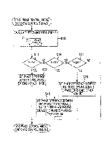
[0040] FIG 4 shows a
flowchart of phase control between the driving signals as a
result of a change of the switching frequency Fs in the case where the
polyphase step-up
converter according to the first embodiment is driven by three phases.
Processes based
on the flowchart are executed in the control unit 12.
[0041] As
shown in FIG. 4, the control unit 12 initially calculates the resonance
frequency Fr (step S10). This calculation is performed by using the above-
described
mathematical expression (1). The resonance frequency Fr depends on the
configuration
of the system 1, so the resonance frequency Fr may be calculated in advance.
[0042]
Subsequently, the control unit 12 executes the frequency determination
step (step S11, step S14, step S17) and the phase difference setting step
(step S13, step S16,
step S19).
[0043] As
described above, in the frequency determination step (step S11, step
S14, step S17), in changing the frequency of each driving signal from the
first frequency to
the second frequency while the N (an integer larger than or equal to two) step-
up circuits
are being driven, it is determined whether the second frequency is M (a
natural number
smaller than or equal to N) times as high as the resonance frequency Fr of the
resonance
circuit provided between the polyphase step-up converter 11 and the load
circuit (for
example, the electric power control unit 20).
[0044] In
the phase difference setting step (step S13, step S16, step S19), when
the second frequency is M times as high as the resonance frequency, the phase
difference
between the plurality of driving signals is set to a phase difference that is
determined in
accordance with the value of M and at which a resonance phenomenon is avoided
(any one
of the phase differences shown in the above-described conditions I to III).
[0045]
Specifically, after completion of step S10, the control unit 12 determines
whether the changed switching frequency Fs of each driving signal coincides
with the
CA 2959780 2017-03-02
13
resonance frequency Fr (step S11). When it is determined in step Sll that the
changed
switching frequency Fs coincides with the resonance frequency Fr (the branch
of YES in
step S11), the control unit 12 sets the phase difference between the three-
phase driving
signals to 120 on the basis of the above-described condition I (step S13),
and ends the
process.
[0046] When
it is determined in step S11 that the switching frequency Fs does not
coincide with the resonance frequency Fr (the branch of NO in step S11), the
control unit
12 determines whether a frequency twice as high as the switching frequency Fs
coincides
with the resonance frequency Fr (step S14). When it is determined in step S14
that the
frequency twice as high as the switching frequency Fs coincides with the
resonance
frequency Fr (the branch of YES in step S14), the control unit 12 sets the
phase difference
between two-phase driving signals out of the three-phase driving signals to a
phase
difference other than 180 on the basis of the above-described condition III
(step S16), and
ends the process.
[0047] When it is
determined in step S14 that the frequency twice as high as the
switching frequency Fs does not coincide with the resonance frequency Fr (the
branch of
NO in step S14), the control unit 12 determines whether a frequency three
times as high as
the switching frequency Fs coincides with the resonance frequency Fr (step
S17). When
it is determined in step S17 that the frequency three times as high as the
switching
frequency Fs coincides with the resonance frequency Fr (the branch of YES in
step S17),
the control unit 12 sets the phase difference between the three-phase driving
signals to a
phase difference other than 120 on the basis of the above-described condition
II (step S19),
and ends the process. When it is determined in step S17 that the frequency
three times as
high as the switching frequency Fs does not coincide with the resonance
frequency Fr (the
branch of NO in step S17), the control unit 12 ends the process without
changing the
current phase difference between the driving signals.
[0048] The
polyphase step-up converter 11 according to the first embodiment
repeats step S11, step S13, step S14, step S16, step S17, step S19 each time
the switching
frequency Fs is changed.
CA 2959780 2017-03-02
14
[0049] In
the polyphase step-up converter 11 according to the first embodiment,
the phase difference between the driving signals is set in accordance with the
flowchart
shown in FIG. 4. This specific example will be described with reference to FIG
5. FIG
shows a timing chart that illustrates a ripple frequency in the case where the
polyphase
5 step-up
converter according to the first embodiment is controlled by three phases. The
example of setting a frequency, shown in FIG 5, is an example of a mode of
setting the
phase difference. When the phase difference is set such that any one of the
conditions I to
IV is satisfied, a phase difference other than that in FIG 5 may also be
employed.
[0050] As
shown in the top graph of FIG. 5, when the switching frequency Fs is
lower than a third of the resonance frequency Fr (in the case of 3Fs < Fr),
the polyphase
step-up converter 11 according to the first embodiment operates while the
phase difference
between the driving signals is set to 120 . In this case, the ripple frequency
Frp includes
only a frequency component (3Fr) that is three times as high as the resonance
frequency Fr.
[0051] As
shown in the above-described condition II, as the switching frequency
Fs reaches a third of the resonance frequency Fr (that is, when 3Fs = Fr), a
resonance
phenomenon occurs if the phase difference between the three-phase driving
signals while
the polyphase step-up converter 11 is being driven by three phases is 120 (=
360 /3).
For this reason, at the time when the frequency three times as high as the
switching
frequency Fs coincides with the resonance frequency Fr, the polyphase step-up
converter
11 changes the phase difference between the driving signals.
[0052]
Specifically, as shown in the second top graph in FIG 5, when the
switching frequency Fs is higher than or equal to a third of the resonance
frequency Fr and
is lower than a half of the resonance frequency Fr (when 2Fs < Fr), the
polyphase step-up
converter 11 operates while the phase difference between the U-phase and V-
phase driving
signals and the phase difference between the V-phase and W-phase driving
signals are set
to 90 and the phase difference between the W-phase and U-phase driving
signals is set to
180 . In this case, the ripple frequency Frp includes a frequency component
(2Fr) twice
as high as the resonance frequency Fr and a frequency component as high as the
resonance
frequency Fr.
CA 2959780 2017-03-02
[0053] As
shown in the above-described condition III, as the switching frequency
Fs reaches a half of the resonance frequency Fr (that is, when 2Fs = Fr), a
resonance
phenomenon occurs if the phase difference between the two W-phase and U-phase
driving
signals while the polyphase step-up converter 11 is being driven by three
phases is 180 (=
5 3600/2).
For this reason, at the time when the frequency twice as high as the switching
frequency Fs coincides with the resonance frequency Fr, the polyphase step-up
converter
11 changes the phase difference between the driving signals.
[0054]
Specifically, as shown in the third top graph in FIG 5, when the switching
frequency Fs is higher than or equal to a half of the resonance frequency Fr
and is lower
10 than the resonance frequency Fr (when Fs < Fr), the polyphase step-up
converter 11
operates while the phase difference between the U-phase and V-phase driving
signals is set
to 900, the phase difference between the U-phase and W-phase driving signals
is set to
240 and the phase difference between the W-phase and U-phase driving signals
is set to
120 . In this case, the ripple frequency Frp includes only a frequency
component as high
15 as the resonance frequency Fr.
[0055] As
shown in the above-described condition I, as the switching frequency
Fs reaches the resonance frequency Fr (that is, when Fs = Fr), a resonance
phenomenon
occurs unless the phase difference between the three-phase driving signals
while the
polyphase step-up converter 11 is being driven is 120 (= 360 /3). For this
reason, at the
time when the switching frequency Fs coincides with the resonance frequency
Fr, the
polyphase step-up converter 11 changes the phase difference between the
driving signals.
[0056]
Specifically, as shown in the bottom graph in FIG 5, when the switching
frequency Fs is higher than or equal to the resonance frequency Fr (when Fs
Fr), the
polyphase step-up converter 11 operates while the phase difference between the
U-phase
and V-phase driving signals, the phase difference between the V-phase and W-
phase
driving signals and the phase difference between the W-phase and U-phase
driving signals
are set to 120 .
[0057] Next,
the case where the polyphase step-up converter 11 is operated while
being driven by two phases will be described. FIG 6 shows a flowchart of phase
control
CA 2959780 2017-03-02
16
between driving signals in the case where the polyphase step-up converter
according to the
first embodiment is controlled by two phases.
[0058] As
shown in FIG. 6, the control unit 12 initially calculates the resonance
frequency Fr (step S20). This calculation is performed by using the above-
described
mathematical expression (1). The resonance frequency Fr depends on the
configuration
of the system 1, so the resonance frequency Fr may be calculated in advance.
[0059]
Subsequently, the control unit 12 executes a frequency determination step
(step S21, step S24) and a phase difference setting step (step S23, step S26).
[0060]
Specifically, after completion of step S20, the control unit 12 determines
whether the switching frequency Fs of each driving signal coincides with the
resonance
frequency Fr (step S21). When it is determined in step S21 that the changed
switching
frequency Fs coincides with the resonance frequency Fr (the branch of YES in
step S21),
the control unit 12 sets the phase difference between the two-phase driving
signals to 180
on the basis of the above-described condition I (step S23), and ends the
process.
[0061] When it is
determined in step S21 that the switching frequency Fs does not
coincide with the resonance frequency Fr (the branch of NO in step S21), the
control unit
12 determines whether a frequency twice as high as the switching frequency Fs
coincides
with the resonance frequency Fr (step S24). When it is determined in step S24
that the
frequency twice as high as the switching frequency Fs coincides with the
resonance
frequency Fr (the branch of YES in step S24), the control unit 12 sets the
phase difference
between the two-phase driving signals to a phase difference other than 180 on
the basis of
. the above-described condition II (step S26), and ends the process. When it
is determined
in step S24 that the frequency twice as high as the switching frequency Fs
does not
coincide with the resonance frequency Fr (the branch of NO in step S24), the
control unit
12 ends the process without changing the current phase difference between the
driving
signals.
[0062] The
polyphase step-up converter 11 according to the first embodiment
repeats step S21, step S23, step S24, step S26 each time the switching
frequency Fs is
changed.
CA 2959780 2017-03-02
17
[0063] Next,
the case where the polyphase step-up converter 11 is operated while
being driven by four phases will be described. FIG. 7 shows a flowchart of
phase control
between driving signals in the case where the polyphase step-up converter
according to the
first embodiment is controlled by four phases.
[0064] As shown in
FIG. 7, the control unit 12 initially calculates the resonance
frequency Fr (step S30). This calculation is performed by using the above-
described
mathematical expression (1). The resonance frequency Fr depends on the
configuration
of the system 1, so the resonance frequency Fr may be calculated in advance.
[0065]
Subsequently, the control unit 12 executes a frequency determination step
(step S31, step S34, step S37, step S40) and a phase difference setting step
(step S33, step
S36, step S39, step S42).
[0066]
Specifically, after completion of step S30, the control unit 12 determines
whether the switching frequency Fs of each driving signal coincides with the
resonance
frequency Fr (step S31). When it is determined in step S31 that the changed
switching
frequency Fs coincides with the resonance frequency Fr (the branch of YES in
step S31),
the control unit 12 sets the phase difference between the four-phase driving
signals to 90
or uses two pairs of driving signals between which the phase difference is set
to 180'on the
basis of the above-described condition I (step S33), and ends the process.
[0067] When
it is determined in step S31 that the switching frequency Fs does not
coincide with the resonance frequency Fr (the branch of NO in step S31), the
control unit
12 determines whether a frequency twice as high as the switching frequency Fs
coincides
with the resonance frequency Fr (step S34). When it is determined in step S34
that the
frequency twice as high as the switching frequency Fs coincides with the
resonance
frequency Fr (the branch of YES in step S34), the control unit 12 sets the
phase difference
between two-phase driving signals out of the four-phase driving signals to a
phase
difference other than 180 (however, it is allowed when the phase difference
between the
four-phase driving signals is 90 ) on the basis of the above-described
condition III (step
S36), and ends the process.
[0068] When
it is determined in step S34 that the frequency twice as high as the
CA 2959780 2017-03-02
18
switching frequency Fs does not coincide with the resonance frequency Fr (the
branch of
NO in step S34), the control unit 12 determines whether a frequency three
times as high as
the switching frequency Fs coincides with the resonance frequency Fr (step
S37). When
it is determined in step S37 that the frequency three times as high as the
switching
frequency Fs coincides with the resonance frequency Fr (the branch of YES in
step S37),
the control unit 12 sets the phase difference between the three-phase driving
signals out of
the four-phase driving signals to a phase difference other than 1200 on the
basis of the
above-described condition III (step S39), and ends the process.
[0069] When
it is determined in step S37 that the frequency three times as high as
the switching frequency Fs does not coincide with the resonance frequency Fr
(the branch
of NO in step S37), the control unit 12 determines whether a frequency four
times as high
as the switching frequency Fs coincides with the resonance frequency Fr (step
S40).
When it is determined in step S40 that the frequency four times as high as the
switching
frequency Fs coincides with the resonance frequency Fr (the branch of YES in
step S40),
the control unit 12 sets the phase difference between the four-phase driving
signals to a
phase difference other than 90 on the basis of the above-described condition
II (step S42),
and ends the process. When it is determined in step S40 that the frequency
four times as
high as the switching frequency Fs does not coincide with the resonance
frequency Fr (the
branch of NO in step S40), the control unit 12 ends the process without
changing the
current phase difference between the driving signals.
[0070] The
polyphase step-up converter 11 according to the first embodiment
repeats step S31, step S33, step S34, step S36, step S37, step S39, step S40,
step S42 each
time the switching frequency Fs is changed.
[0071]
According to the above description, in the polyphase step-up converter 11
according to the first embodiment, when it is determined that a resonance
phenomenon
occurs as a result of coincidence of the ripple frequency superimposed on an
output voltage
on the basis of the switching frequency of each driving signal and the phase
difference
between the driving signals with the resonance frequency of the resonance
circuit, the
ripple frequency is shifted from the resonance frequency by changing the phase
difference
CA 2959780 2017-03-02
19
between the driving signals. Thus, the polyphase step-up converter 11
according to the
first embodiment is able to avoid a resonance phenomenon that occurs in the
resonance
circuit without providing a circuit or element for shifting the resonance
frequency in the
resonance circuit. That is, with the use of the polyphase step-up converter 11
according
to the first embodiment, it is possible to avoid a resonance phenomenon that
occurs in the
system without increasing the volume or weight of the system.
[0072]
Particularly, in order to reduce the size of the polyphase step-up converter,
it is effective to increase the switching frequency Fs of each driving signal.
However, if
the switching frequency is attempted to be made higher than the resonance
frequency Fr of
the resonance circuit that is provided in a path that connects the polyphase
step-up
converter 11 to the electric power control unit 20, an output voltage
excessively increases
unless a resonance phenomenon in the resonance circuit is avoided, so there is
an
inconvenience that measures for handling an increase in the output voltage are
taken in the
electric power control unit 20. For the above reasons, when the switching
frequency is
increased, there is a great significance of avoiding a resonance phenomenon of
the
resonance circuit while minimizing the volume and weight of the system.
[0073] The
invention made by the inventors is specifically described above on the
basis of the embodiment; however, the invention is not limited to the
embodiment
described above. Of course, various modifications are applicable without
departing from
the scope of the invention.