Note: Descriptions are shown in the official language in which they were submitted.
CA 2959819 2017-03-02
DESCRIPTION
TITLE OF THE INVENTION
A Drive Circuit for Transmitting Data Signals on Power Wire
TECHNICAL FIELD OF THE INVENTION
This invention relates to the signal transmission technology field, and
particularly relates to a drive circuit for transmitting data signals on power
wire.
BACKGROUND OF THE INVENTION
Currently, in many application fields, signals are transmitted to the part of
receiving signals through the special signal line, such setting needs special
signal
line, and causes many signal connection lines on the interface, wiring is
difficult,
installation and decoration is inconvenient, the line cost is high, and the
workload is
heavy; the wiring of circuit boards is crowded, and sometimes there are too
many
liens to add the wiring layer.
How to use the power wire to transmit data signals so as to save the lines
and reduce the complexity of wiring is a pressing problem.
BRIEF SUMMARY OF THE INVENTION
This invention provides a drive circuit for transmitting data signals on
power wire, and it, by controlling the connection and disconnection of
switching
circuit, indirectly controls the voltage outputted by DC power supply to the
receiving
terminal, so as to transmit the information, and the receiving terminal
collects the
data signals according to the voltage change.
To achieve such purpose, this invention adopts the following technical plan:
A drive circuit for transmitting data signals on power wire, which comprises:
A DC power supply, used to convert the input alternating current into direct
current;
1
CA 2959819 2017-03-02
A switching circuit, connected between DC power supply and receiving
terminal;
A voltage division clamping circuit, connected between DC power supply
and receiving terminal;
And a control circuit, connected to the said switching circuit, so as to
control the connection and disconnection of the said switching circuit; when
the
switching circuit is connected, the said DC power supply applies a higher
voltage to
the receiving terminal through the said switching circuit, and when the
switching
circuit is disconnected, the said DC power supply applies a lower voltage to
the
receiving terminal through the said voltage division clamping circuit.
Wherein, the said switching circuit is a NMOS tube, the source electrode
of the said NMOS is connected to the negative electrode of the said DC power
supply, the drain electrode of the said NMOS tube is connected to the control
signal
output end of the said control circuit; and the input end of the said
receiving terminal
is connected to the positive electrode of the said DC power supply; or
The said switching circuit is a PMOS tube, the source electrode of the said
PMOS tube is connected to the positive electrode of the said DC power supply,
the
drain electrode of the said PMOS tube is connected to the input end of the
said
receiving terminal, the grid electrode of the said PMOS tube is connected to
the
control signal output end of the said control circuit; and the output end of
the said
receiving terminal is connected to the negative electrode of the said DC power
supply.
Wherein, the said control circuit is a microcontroller unit, VCC end and
GND end of the said microcontroller unit are connected to a voltage regulator
diode
D2 in parallel, VCC end of the said microcontroller unit is connected to the
negative
2
CA 2959819 2017-03-02
electrode of the said voltage regulator diode D2, and GND end of the said
microcontroller unit is connected to the positive electrode of the said
voltage
regulator diode D2.
Wherein, the said voltage division clamping circuit contains the voltage
divider resistor R2 and the voltage regulator diode D3;
If the switching circuit is a NMOS tube, the negative electrode of the said
voltage regulator diode D3 is connected to the positive electrode of DC power
supply,
the positive electrode of the voltage regulator diode D3 is connected to one
end of
the said voltage divider resistor R2 and the output end of the receiving
terminal, the
other end of the voltage divider resistor R2 is connected to VCC end of the
microcontroller unit, and GND end of the microcontroller unit is connected to
the
negative electrode of DC power supply;
If the switching circuit is a PMOS tube, one end of the said voltage divider
resistor R2 is connected to GND end of the microcontroller unit, the other end
of the
said voltage divider resistor R2 is connected to the negative electrode of the
voltage
regulator diode D3 and the input end of the receiving terminal, the positive
electrode
of the said voltage regulator diode D3 is connected to the negative electrode
of DC
power supply; and VCC end of the microcontroller unit is connected to the
positive
electrode of DC power supply.
Wherein, the said drive circuit also includes a filter circuit, the said
filter
circuit contains the resistor R3 and the capacitor C3, one end of the said
resistor R3
and one end of the capacitor C3 are connected to the positive electrode of DC
power
supply, and the other end of the said resistor R3 and the other end of
capacitor C3
are connected to the negative electrode of DC power supply;
3
CA 2959819 2017-03-02
VCC end and GND end of the said microcontroller unit are connected to
the resistor R1 and the capacitor C1 in parallel;
The side of the said receiving terminal connected to the voltage division
clamping circuit is connected to the capacitor C2 in parallel and connected to
the
diode D1 in series; if the said switching circuit is a NMOS tube, the output
end of the
receiving terminal is connected to the positive electrode of the diode D1, the
negative electrode of the diode D1 is connected to one end of the capacitor C2
and
the positive electrode of the voltage regulator diode D3, and the other end of
the
capacitor C2 is connected to the input end of the receiving terminal; if the
said
switching circuit is a PMOS tube, the input end of the said receiving terminal
is
connected to the negative electrode of the diode D1, the positive electrode of
the
diode D1 is connected to the negative electrode of the voltage regulator diode
D3
and one end of the capacitor C2, and the other end of the capacitor C2 is
connected
to the output end of the receiving terminal.
Wherein, the said DC power supply is a constant-current source.
Wherein, the said receiving terminal is a LED bar which is connected to N
LED beads in series or in parallel, the positive electrode of the said LED bar
is the
input end of the receiving terminal, and the negative electrode of the said
LED bar is
the output end of the receiving terminal; or
The said receiving terminal is at least two LED bars which are connected
to N LED beads in series or in parallel, the end of the positive electrode of
each said
LED bar connected in parallel is the input end of the receiving terminal, and
the end
of the negative electrode of each said LED bar connected in parallel is the
output
end of the receiving terminal;
Wherein, N is a positive integer.
4
CA 2959819 2017-03-02
Wherein, the said DC power supply is AC-DC constant-voltage source.
Wherein, the said receiving terminal is a LED bar which is connected to
the limited current circuit in series and is connected to N LED beads in
series or in
parallel, the positive electrode of the said LED bar is the input end of the
receiving
terminal, the negative electrode of the said LED bar is connected to the input
end of
the limited current circuit, and the output end of the said limited current
circuit is the
output end of the said receiving terminal; or
The said receiving terminal is at least two LED bars which are connected
to the limited current circuit in series and are connected to N LED beads in
series or
in parallel, the end of the positive electrode of each said LED bar connected
in
parallel is the input end of the receiving terminal, the negative electrode of
each said
LED bar is connected to the input end of a limited current circuit, and the
end of the
output end of each said limited current circuit connected in parallel is the
output end
of the said receiving terminal;
Wherein, N is a positive integer.
Wherein, the said limited current circuit comprises the resistor R4, the
resistor R5, the triode Q1 and the triode Q2, one end of the said resistor R4
and the
collector electrode of the said triode Q2 are connected to the input end of
the limited
current circuit, the other end of the said resistor R4 is connected to the
base
electrode of the said triode Q2 and the collector electrode of the said triode
Q1, the
emitter electrode of the said triode Q2 is connected to the base electrode of
the said
triode Q1 and one end of the said resistor R5, and the emitter electrode of
the said
triode Q1 and the other end of the said resistor R5 are connected to the
output end
of the limited current circuit.
CA 2959819 2017-03-02
Compared with the prior art, the advantageous effect of this invention is:
this invention changes the voltage applied by DC power supply to both ends of
the
receiving terminal by controlling the connection and disconnection of switch
control
circuit, and when the said switch control circuit is connected, the voltage
across the
said receiving terminal is high voltage, and when the said switch control
circuit is
disconnected, the voltage across the receiving terminal will be clamped at low
voltage through the voltage division clamping circuit, and by controlling the
connection and disconnection of the switch control circuit, this invention
indirectly
controls the voltage outputted by DC power supply to the receiving terminal so
as to
transmit the information, and the receiving terminal collects the data signals
according to the voltage change, so as to transmit the data signals on DC
power wire.
BRIEF DESCRIPTION OF THE DRAWINGS
Fig. 1 is the structure diagram I of the drive circuit for transmitting data
signals on power wire provided by this invention.
Fig. 2 is the structure diagram II of the drive circuit for transmitting data
signals on power wire provided by this invention.
Fig. 3 is the circuit diagram I of the drive circuit for transmitting data
signals on power wire provided by this invention.
Fig. 4 is the circuit diagram II of the drive circuit for transmitting data
signals on power wire provided by this invention.
Fig. 5 is the circuit diagram III of the drive circuit for transmitting data
signals on power wire provided by this invention.
Fig. 6 is the circuit diagram IV of the drive circuit for transmitting data
signals on power wire provided by this invention.
6
CA 2959819 2017-03-02
Fig. 7 is the example diagram of the drive circuit for transmitting data
signals on power wire provided by this invention connected to mini light bar.
Fig. 8 is the example diagram of the drive circuit for transmitting data
signals on power wire provided by this invention connected to LED bar of LED
bead.
Fig. 9 is the circuit diagram of a limited current circuit provided by this
invention.
Fig. 10 is the definition of a data Bit0 and data Bit1 provided by this
invention.
Fig. 11 is a data frame format provided by this invention.
DETAILED DESCRIPTION OF THE INVENTION
To make the technical problems solved by this invention, the adopted
technical plan and the achieved technical effect clearer, the following will
present
further detailed description about the technical plan of this invention's
example in
conjunction with the drawings. Obviously, the described example is only part
of the
examples of this invention and not all examples. All the other examples
obtained by
the technicians of this field based on this invention's examples under the
condition of
no creative work belong to the protection scope of this invention.
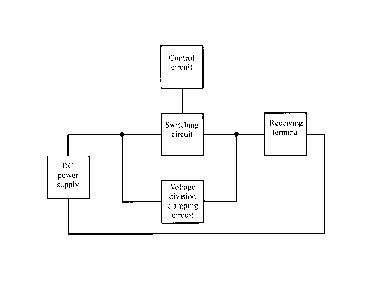
Please refer to Fig. 1-2, Fig. us the structure diagram I of the drive circuit
for transmitting data signals on power wire provided by this invention; Fig. 2
is the
structure diagram ll of the drive circuit for transmitting data signals on
power wire
provided by this invention; a drive circuit for transmitting data signals on
power wire,
which comprises: a DC power supply, used to convert the input alternating
current
into direct current; a switching circuit, connected between DC power supply
and
receiving terminal; a voltage division clamping circuit, connected between DC
power
supply and receiving terminal; and a control circuit, connected to the said
switching
7
CA 2959819 2017-03-02
circuit, so as to control the connection and disconnection of the said
switching circuit;
when the switching circuit is connected, the said DC power supply applies a
higher
voltage to the receiving terminal through the said switching circuit, and when
the
switching circuit is disconnected, the said DC power supply applies a lower
voltage
to the receiving terminal through the said voltage division clamping circuit.
The
difference between Fig. 1 and Fig. 2 is: in Fig. 1, DC power supply passes
through
the switch circuit and then goes to the receiving terminal; while in Fig. 2,
DC power
supply passes through the receiving terminal and then goes to the switching
circuit,
and the voltage division clamping circuit is adjusted appropriately. It needs
to be
explained that, the higher voltage and lower voltage in this example are
relative to
them, namely, the voltage applied to the receiving terminal by the said DC
power
supply through the said switch circuit when the switch circuit is connected is
higher
than the voltage applied to the receiving terminal by the said DC power supply
through the said voltage division clamping circuit when the switch circuit is
disconnected.
The example of this invention, by controlling the connection and
disconnection of control switch circuit, indirectly controls the voltage
applied by DC
power supply to the receiving terminal, so as to transmit the information, and
the
receiving terminal collects the data signals according to the voltage change,
so as to
transmit the data signals on DC power wire.
Please refer to Fig. 3-6, Fig. 3 and Fig. 4 are NMOS-based drive circuit,
while Fig. 5 and Fig. 6 are PMOS-based drive circuit.
As shown in Fig. 3 and Fig. 4, the said switch circuit is a NMOS tube, the
source electrode (S-electrode) of the said NMOS is connected to the negative
8
CA 2959819 2017-03-02
electrode of the said DC power supply, the drain electrode (D-electrode) of
the said
NMOS tube is connected to the output end of the said receiving terminal, the
grid
electrode (G-electrode) of the said NMOS tube is connected to the control
signal
output end of the said control circuit; and the input end of the said
receiving terminal
is connected to the positive electrode of the said DC power supply; or
As shown in Fig. 5 and Fig. 6, the said switching circuit is a PMOS tube,
the source electrode (S-electrode) of the said PMOS tube is connected to the
positive electrode of the said DC power supply, the drain electrode (D-
electrode) of
the said PMOS tube is connected to the input end of the said receiving
terminal, the
grid electrode (G-electrode) of the said PMOS tube is connected to the control
signal
output end of the said control circuit; and the output end of the said
receiving
terminal is connected to the negative electrode of the said DC power supply.
The said control circuit is a microcontroller unit (MCU), VCC end and GND
end of the said microcontroller unit are connected to a voltage regulator
diode D2 in
parallel, VCC end of the said microcontroller unit is connected to the
negative
electrode of the said voltage regulator diode 02, and GND end of the said
microcontroller unit is connected to the positive electrode of the said
voltage
regulator diode D2. It needs to be explained that, the voltage regulator diode
D2 has
VCC end and GND end of the microcontroller unit clamped at 3.3V-5V, so as to
ensure normal work of the microcontroller unit.
The said voltage division clamping circuit contains the voltage divider
resistor R2 and the voltage regulator diode D3;
9
CA 2959819 2017-03-02
As shown in Fig. 3 and Fig. 4, if the switching circuit is a NMOS tube, the
negative electrode of the said voltage regulator diode D3 is connected to the
positive
electrode of DC power supply, the positive electrode of the voltage regulator
diode
D3 is connected to one end of the said voltage divider resistor R2 and the
output end
of the receiving terminal, the other end of the voltage divider resistor R2 is
connected
to VCC end of the microcontroller unit, and GND end of the microcontroller
unit is
connected to the negative electrode of DC power supply;
As shown in Fig. 5 and Fig. 6, if the switching circuit is a PMOS tube, one
end of the said voltage divider resistor R2 is connected to GND end of the
microcontroller unit, the other end of the said voltage divider resistor R2 is
connected
to the negative electrode of the voltage regulator diode D3 and the input end
of the
receiving terminal, the positive electrode of the said voltage regulator diode
D3 is
connected to the negative electrode of DC power supply; and VCC end of the
microcontroller unit is connected to the positive electrode of DC power
supply.
As shown in Fig. 3-6, the said drive circuit also includes a filter circuit,
the
said filter circuit contains the resistor R3 and the capacitor C3, one end of
the said
resistor R3 and one end of the capacitor C3 are connected to the positive
electrode
of DC power supply, and the other end of the said resistor R3 and the other
end of
the capacitor C3 are connected to the negative electrode of DC power supply.
It
needs to be explained that, since the capacitor C3 is to filter DC power
supply, the
voltage / current between positive electrode and negative electrode of DC
power
supply is stable, and the function of R3 is to make the capacitor discharge
path when
DC power supply is disconnected, the capacitor C3 discharges electricity from
the
resistor R3, and because the capacitor C3 starts to supply power after DC
power
CA 2959819 2017-03-02
supply is disconnected, if just relying on the power consumption of the load
on the
receiving terminal, it takes a very long time to finish discharging the
electricity, and if
it is slow to discharge the electricity, when the load on the receiving
terminal is not
powered off thoroughly, if the system is electrified again, the load on the
receiving
terminal might work abnormally.
Preferably, VCC end and GND end of the microcontroller unit are
connected to the resistor R1 and the capacitor Cl in parallel; since the
capacitor C1
is to filter DC power supply, the voltage / current between VCC end and GND
end of
the microcontroller unit is stable, and the function of R1 is to make the
capacitor
discharge path when DC power supply is disconnected, the capacitor C1
discharges
electricity from the resistor R1, and because the capacitor Cl starts to
supply power
after DC power supply is disconnected , if just relying on the power
consumption of
the microcontroller unit, it takes a very long time to finish discharging the
electricity,
and if it is slow to discharge the electricity, when the microcontroller unit
is not
powered off thoroughly, if the system is electrified again, the
microcontroller unit
might work abnormally.
The side of the said receiving terminal connected to the voltage division
clamping circuit is connected to the capacitor C2 in parallel and connected to
the
diode D1 in series; if the said switching circuit is a NMOS tube, the output
end of the
receiving terminal is connected to the positive electrode of the diode D1, the
negative electrode of the diode D1 is connected to one end of the capacitor C2
and
the positive electrode of the voltage regulator diode D3, and the other end of
the
capacitor C2 is connected to the input end of the receiving terminal; if the
said
switching circuit is a PMOS tube, the output end of the said receiving
terminal is
11
CA 2959819 2017-03-02
connected to the negative electrode of the diode D1, the positive electrode of
the
diode D1 is connected to the negative electrode of the voltage regulator diode
D3
and one end of the capacitor C2, and the other end of the capacitor C2 is
connected
to the output end of the receiving terminal. The diode D1 is used to control
the
current direction, while the capacitor C2 is used to stabilize the voltage
across the
receiving terminal.
The basic principle of the example of this invention is: when the
microcontroller unit controls the NMOS to be connected, the current flows from
the
positive electrode of DC power supply to the receiving terminal, and then to
the
negative electrode of DC power supply, and the voltage across the receiving
terminal
is high voltage; when the microcontroller unit controls the NMOS to be
disconnected,
the current flows from the positive electrode of DC power supply to the
receiving
terminal, the diode D'1, the resistor R2, the voltage regulator tube D2, and
then to the
negative electrode of DC power supply, and due to the action of the voltage
regulator
tube D3, the voltage across the receiving terminal is clamped at low voltage,
as
shown in Fig. 3 and Fig. 4, this invention, by controlling the connection and
disconnection of NMOS, indirectly controls the voltage outputted by DC power
supply, so as to transmit the information, and the receiving terminal collects
the data
signals according to the voltage change. Or when the microcontroller unit
controls
PMOS to be connected, the current flows from the positive electrode of DC
power
supply to the receiving terminal, and then to the negative electrode of DC
power
supply, and the voltage across the receiving terminal is high voltage; when
the
microcontroller unit controls PMOS to be disconnected, the current flows from
the
positive electrode of DC power supply to the diode D2, the resistor R2, the
diode D1,
the receiving terminal, and then to the negative electrode of DC power supply,
and
12
CA 2959819 2017-03-02
due to the action of the voltage regulator tube D3, the voltage across the
receiving
terminal is clamped at low voltage, as shown in Fig. 3 and Fig. 4, this
invention, by
controlling the connection and disconnection of PMOS, indirectly controls the
voltage
outputted by DC power supply, so as to transmit the information, and the
receiving
terminal collects the data signals according to the voltage change.
Wherein, the said DC power supply is constant-current source, as shown
in Fig. 4 and Fig. 6. The said receiving terminal is a LED bar which is
connected to N
LED beads in series or in parallel, the positive electrode of the said LED bar
is the
input end of the receiving terminal, the negative electrode of the said LED
bar is the
output end of the receiving terminal, and N is a positive integer. As another
example,
the said receiving terminal is at least two LED bars which are connected to N
LED
beads in series or in parallel, the end of the positive electrode of each said
LED bar
connected in parallel is the input end of the receiving terminal, the end of
the
negative electrode of each said LED bar connected in parallel is the output
end of
the receiving terminal, and N is a positive integer.
Wherein, the said DC power supply is AC-DC constant-voltage source, as
shown in Fig. 3 and Fig. 5. The said receiving terminal is a LED bar which is
connected to the limited current circuit in series and is connected to N LED
beads in
series or in parallel, the positive electrode of the said LED bar is the input
end of the
receiving terminal, the negative electrode of the said LED bar is connected to
the
input end of the limited current circuit, and the output end of the said
limited current
circuit is the output end of the said receiving terminal. As another example,
the said
receiving terminal is at least two LED bars which are connected to the limited
current
circuit in series and are connected to N LED beads in series or in parallel,
the end of
13
CA 2959819 2017-03-02
the positive electrode of each said LED bar connected in parallel is the input
end of
the receiving terminal, the negative electrode of each said LED bar is
connected to
the input end of a limited current circuit, and the end of the output end of
each said
limited current circuit connected in parallel is the output end of the said
receiving
terminal.
Fig. 7-8 show a drive circuit for transmitting data signals on power wire
provided by this invention, and it can be applied to mini light bar or LED bar
of LED
bulb, so that the mini light bar or LED bar of LED bulb will have good
changing effect.
Fig. 9 shows the circuit diagram of a limited current circuit provided by this
invention, and the said limited current circuit comprises the resistor R4, the
resistor
R5, the triode Q1 and the triode Q2, one end of the said resistor R4 and the
collector
electrode of the said triode Q2 are connected to the input end of the limited
current
circuit, the other end of the said resistor R4 is connected to the base
electrode of the
said triode Q2 and the collector electrode of the said triode Q1, the emitter
electrode
of the said triode Q2 is connected to the base electrode of the said triode Q1
and
one end of the said resistor R5, and the emitter electrode of the said triode
Q1 and
the other end of the said resistor R5 are connected to the output end of the
limited
current circuit.
That is to say, the DC power supply can be constant-current source or AC-
DC constant-voltage source.
If the DC power supply is AC-DC constant-voltage source, the alternating
current outputs constant voltage after going through AC-DC constant-voltage
source.
The end of each LED bar needs to be connected to the limited current circuit,
as
14
CA 2959819 2017-03-02
shown in Fig. 1 and Fig. 3. When NM1 or PM1 is connected, both ends of LED bar
are connected constantly to the high voltage Uon=U-Uds (subtract the break-
over
voltage of one MOS tube from the regulated voltage), and the LED bead will
give out
light. However, the clamping voltage among the beads have difference, the
total
clamping voltage of each bar is different. Take 24 lights as an example, the
standard
voltage is 80V, the voltage of some bars is about 80V, the voltage of other
bars
might be only 70V, and because the branch voltage of bead on such light bar is
,
greater than the normal clamping voltage 400mV, the current through the chip
is too
high, and the chip will be burnt out easily, a limited current circuit is
added on the
end of LED bar to absorb the excess voltage. When NMOS or PMOS is
disconnected, due to the existence of the voltage regulator diode D3, the
voltage
across LED light is clamped at low voltage, and the LED bar will not give out
light.
Then the current IR2=1D3+1LED, and the resistance R2= (U-UD2-UD3)/IR2.
If the DC power supply is constant-current source, the alternating current
outputs constant current after going through constant-current drive, and the
structure
of drive circuit is unchanged and is the same as the drive circuit of constant-
voltage
source. The end of each LED bar does not need to be connected to the limited
current circuit, as shown in Fig. 2 and Fig. 4. When NMOS or PMOS is
connected,
both ends of LED bar are connected constantly to constant-current output, LED
bead
will give out light, and the voltage across the LED bar is determined by
multiplying
the number of the beads by the clamping voltage of LED bead. When NMOS or
PMOS is disconnected, the voltage across the LED bar is clamped at the low
voltage
UD3 and it will not give out light. As the resistance R2 = (U-UD2-UD3)/IR2, at
the
moment when MOS tube is closed, the high ILED applies to both ends of R2
suddenly, and the resistance voltage UR2 rises suddenly. At such moment, it
needs
CA 2959819 2017-03-02
to select higher capacitor C3 to stabilize the voltage, and when UR2>UC3, the
capacitor C3 is charging, and it is only required to ensure that when NMOS or
PMOS
is disconnected, the voltage across the capacitor C3 is basically unchanged.
Therefore, the calculation method of the divider resistance of R2 is
consistent with
the drive circuit of constant-voltage source.
As an example, the drive circuit provided by this invention can be used to
send data signals to LED bar, the definition of data Bit0 and data Bit1 is
shown in Fig.
10, the data of continuous lps low and 4ps high means Bit , the data of
continuous
2ps low and 4ps high means Bit1, and user can also define other Bit() and
Bit1. This
invention transmits data signals by controlling the connection and
disconnection of
MOS through the microcontroller unit, and the data frame format is shown in
Fig. 9.
In one data frame, the preamble + head + node RGB data + check bit (bit0)
constitute a complete frame of data, one frame contains 512 nodes at most, and
it
can be used to drive 512 RGB tri-colored LED beads, the chip in LED bead
receives
the data signals sent by the microcontroller unit, and controls the gray scale
of LED
bead according to the data signals.
Wherein, the preamble is 8bit data, the head is 4bit data, and they
represent the data frame type, as shown in Table 1.
Table 1 Correspondence Between Head and Data Frame Type
Header Type Define Description
4'b1010 RGB_FRAME Data frame, {R, G, B}=Data #1[23:0]
4'b1000 PROG _ID Burning chip address CHIPID, Data #1[7:0]
Test frame, not needing to match the chip address,
4'b0110 CURRJT
directly change RGB gray scale.
16
CA 2959819 2017-03-02
RGB data totally has 25 bits (from high bit to low bit, the high bit is sent
first), among which, 24 bits are RGB three-channel gray data, 8bit 256-scale
gray for
each channel, and the final 1 bit0 is check bit.
In conclusion, for a drive circuit for transmitting data signals on power wire
provided by this invention, when the microcontroller unit controls NMOS/PMOS
tube
to be connected, the voltage across the receiving terminal is high voltage;
when the
microcontroller unit controls NMOS/PMOS tube to be disconnected, due to the
action
of the voltage divider resistor R2 and the voltage regulator tube D3, the
voltage
across the receiving terminal is clamped at low voltage. By controlling the
connection
and disconnection of NMOS/PMOS tube, the drive circuit indirectly controls the
voltage applied by DC power supply to the receiving terminal, so as to
transmit the
information, and the receiving terminal collects the data signals according to
the
voltage change, so as to transmit the data signals on DC power wire. The drive
circuit provided by this invention can be used to drive LED beads connected in
series
or in parallel, and each LED bead connected in series or in parallel can
collect data
signals according to the voltage change, so as to change the gray scale of LED
bead.
The above describes this invention's technical principle in combination
with examples. These descriptions just explain this invention's principle, and
cannot
be interpreted in any manner as the limitation for protection scope of this
invention.
The drawings only show one of the implementation ways of this invention, and
the
actual structure is not limited to it. On the basis of such interpretation,
technicians of
this field can associate with other specific embodiments of this invention
without
creative work, and these embodiments will fall into the protection scope of
this
invention.
17