Note: Descriptions are shown in the official language in which they were submitted.
CA 02960115 2017-03-02
WO 2016/037175
PCT/US2015/048877
1
TITLE OF INVENTION
Nano-Structured Porous Thermoelectric Generators
CROSS-REFERENCE TO RELATED APPLICATIONS
[0001] This Application claims the benefit of United States Provisional
Patent
Application Number 62/046,434, filed September 5, 2014, incorporated herein in
its entirety
by reference.
STATEMENT REGARDING FEDERALLY SPONSORED RESEARCH OR
DEVELOPMENT
[0002] Not Applicable
BACKGROUND OF THE INVENTION
1. Field of Invention
[0003] The present general inventive concept relates to the preparation and
use of
thermoelectric materials and more particularly to methods and processes to
fabricate doped
thermoelectric generators, especially doped silicon-based thermoelectric
generators.
2. Description of the Related Art
[0004] Semiconductive materials that exhibit the Seebeck and Peltier
effects in the
presence of a temperature gradient are useful for the production of
electricity from waste
heat. Semiconductive materials which move heat from one side to the other when
presented
with an electrical charge from one side to the other are useful for cooling
and exhibit the
Seebeck effect in the form of the Peltier phenomena. The class of
semiconductive materials
exhibiting the Seebeck and Peltier effect is hereinafter called
thermoelectrics or
thermoelectric materials.
CA 02960115 2017-03-02
WO 2016/037175
PCT/US2015/048877
2
[0005] A number of contemporary thermoelectrics comprise alternating P-type
and
N-type semiconductor elements connected by metallic connectors. Many
contemporary
thermoelectrics present various disadvantages, including, in some instances,
high material
costs, high costs of production, difficulty of manufacture, the use of rare
elements, the use of
potentially carcinogenic or toxic substances, and limited formability.
[0006] To achieve a high level of conversion, both a high thermoelectric
figure-of-
merit (ZT) and a high operating temperature are required.
[0007] The Seebeck Coefficient (S) of a material is a measurement of the
magnitude
of an induced thermoelectric voltage in response to a temperature difference
across that
material. Optimally, a highly efficient thermoelectric material should have a
high Seebeck
Coefficient, high electrical conductivity, and low thermal conductivity and be
able to operate
at high temperatures, meaning it should have a low coefficient of thermal
expansion. See,
e.g., Ci et al., Materials Letters 65, 1618-1620 (2011). Other considerations
arise as well.
For instance in order to sustain a high temperature difference from one side
to the other a low
coefficient of thermal expansion, low Poisson ratio and high strength are
desirable. It is
desirable that a thermoelectric material be susceptible to being worked to
construct planar
and complex net-shaped objects that can be fitted into locations where they
may be used to
recover waste heat. Such a thermoelectric material should have a cross section
with
properties to maintain a sufficiently high temperature differential between
the two opposing
sides in order to generate voltage efficiently. It is also desirable that a
thermoelectric material
have high tensile strength, have resistance to thermal shock, and be formable
into layers to
allow the creation of graded indices for electrical, thermal, or other
parameters¨allowing
one thermoelectric material to serve as the basis for a range of
thermoelectric devices.
[0008] The thermoelectric figure-of-merit, ZT, for a thermoelectric
material (TEMat)
is a measure of its efficiency. Z is calculated by multiplying electrical
conductivity (s) and
Seebeck Coefficient (S) squared and dividing by thermal conductivity (k), or
Z= S2G/ k, and
ZT is calculated by multiplying Z with absolute temperature (in Kelvin). To
achieve a high
power factor, it is therefore desirable to have a TEMat with low thermal
conductivity, high
CA 02960115 2017-03-02
WO 2016/037175
PCT/US2015/048877
3
electrical conductivity, high Seebeck Coefficient, and with a high temperature
operating
capability (i.e., a sustainable temperature difference across its structure or
DT capability).
[0009] But potentially exploiting a TEMat's ZT is more than materials
science.
Successful exploitation will need to combine brittle material engineering
practices as
TEMats, as a material class, are very brittle (i.e., low fracture toughness).
A prerequisite to
exploiting a TEMat high temperature capability and its ZT is it must be able
to also
mechanically withstand a large DT in service. This in turn results in a need
for the TEMat to
have a minimum coefficient of thermal expansion (CTE) and maximum tensile
strength
(STen). Lastly, from a perspective of size, a larger TEMat component or "leg"
will promote
the ability to achieve a larger DT (presuming it does not mechanically fail);
this is an
important issue for achieving cold temperatures too.
[0010] Incumbent technologies offer little hope of making low cost thick
structures
able to operate at high temperatures with high unaided DT and attractive power
factors.
Traditional and new approaches to making thermoelectric generators (TEGs) are
all flawed
by fundamental and seemingly intractable challenges, such as high cost, high
CTE, limited to
thin planer structures, low S, low electrical conductivity, low mechanical
strength, or use of
rare and costly materials, or combinations thereof Many of those same issues
limit the
ability to achieve colder temperatures with thermoelectric coolers (TECs).
[0011] Also, thermoelectric materials, as a material class, are very
brittle. Therefore,
it is also desirable to be able to fashion a thermoelectric material with
reduced brittleness.
[0012] An ideal pathway for making thermoelectric devices would include a
way to
obtain nano sized equiaxed silicon grains that could be formed into robust
large shapes with
large cross sections and a nano structured morphology, so to achieve or
promote a low CTE,
a low value for k, very high values for s, gain high S values, and high
operating temperature
capability.
[0013] Many of the recent efforts and developments in this field have
focused on
nanowires and MEMS, which have brought forward announcements confirming
exceptionally high power factors with very high efficiencies in converting
waste heat to
CA 02960115 2017-03-02
WO 2016/037175
PCT/US2015/048877
4
electricity. Unfortunately, these structures are expensive and cannot be
practically made in
the thick cross sections required to maintain a large unaided or largely
unaided AT. Many of
the results reported used aggressive heat exchange apparatus to maintain a
high AT. In many
or most cases, these aggressive heat exchange apparatus are also necessary to
limit the AT in
order to avoid catastrophic thermomechanical failure of the thermoelectric
materials.
[0014] Some thermoelectric generators employ compounds and elements such
as
tellurium or rare earth metals¨many of which are scarce, sourced from only a
few locations.
For operators working in North America, many such materials must be imported
(for
example, most rare earth metals at this time are imported from China). It is
desirable to have
a thermoelectric material that does not require tellurium, rare earth metals,
and similarly rare
component materials.
[0015] Wang et al. ("Effect of Grain Sizes and Shapes on Phonon Thermal
Conductivity of Bulk Thermo Electric Materials," Journal of Applied Physics
110, 024312
[2011]) teach that silicon's thermal conductivity is insensitive to grain size
until the grain
sizes are reduced to quite a bit less than a micron, and then falls
precipitously from about 600
nm to 5 nm with thermal conductivity falling to less than 0.4 W/mK. But they
only address a
"bulk" material. They do not describe methods or sources for a silicon bulk
material with a
grain size in the range of a few or tens of nanometers, but conclude that only
by reducing the
grain size can one obtain silicon with very low thermal conductivity.
[0016] U.S. Patent No. 8,334,194, issued to Jonczyk and Rand, discloses
methods and
apparatus for fabricating a semiconductor sheet. In one aspect, a method for
fabricating a
semiconductor wafer includes applying a layer of semiconductor material across
a portion of
a setter material, introducing the setter material and the semiconductor
material to a
predetermined thermal gradient to form a melt, wherein the thermal gradient
includes a
predetermined nucleation and growth region, and forming at least one local
cold spot in the
nucleation and growth region to facilitate inducing crystal nucleation at the
at least one
desired location.
[0017] U.S. Patent No. 9,011,763, issued to Chen et al., discloses
nanocomposite
thermoelectric materials that exhibit enhanced thermoelectric properties. The
nanocomposite
CA 02960115 2017-03-02
WO 2016/037175
PCT/US2015/048877
materials include two or more components, with at least one of the components
forming
nano-sized structures within the composite material. The components are chosen
such that
thermal conductivity of the composite is decreased without substantially
diminishing the
composite's electrical conductivity. Suitable component materials exhibit
similar electronic
band structures. For example, a band-edge gap between at least one of a
conduction band or a
valence band of one component material and a corresponding band of the other
component
material at interfaces between the components can be less than about 5kBT,
wherein kB is the
Boltzman constant and T is an average temperature of said nanocomposite
composition.
BRIEF SUMMARY OF THE INVENTION
[0018] Silicon has a high Seebeck Coefficient, a high capability to work
at a range of
temperatures, and the ability to be tailored as a semiconductor. U.S. Patent
6,638,491 teaches
a safe and economical method for nano-sizing silicon safely and economically.
What is
needed is a silicon-based material with a low thermal conductivity.
[0019] Disclosed herein are methods and processes to fabricate
thermoelectric
materials and more particularly methods and processes to fabricate doped
silicon-based
semiconductive materials to use as thermoelectrics in the production of
electricity from
recovered waste heat.
[0020] The challenge of making a very effective thermoelectric device (for
generating
electricity or for cooling by the Seebeck and Peltier effects, respectively)
with silicon
depends upon several variables that relate to optimization per the Seebeck
equation. In
various example embodiments of the present general inventive concept,
fabrication of these
effective silicon-based thermoelectric devices involves: doping for high
electrical
conductivity for both P-type and N-type by doping from column III and column V
of the
periodic chart respectively, as is done for semiconductor applications; doping
within the
discipline of otherwise very high purity to maintain high values for the
Seebeck Coefficient;
utilizing the ability to manipulate silicon at very high temperatures; and
reducing the thermal
conductivity by exploiting the quantum size effect for blocking phonons while
maintaining
high electrical conductivity. The present general inventive concept
accomplishes all of this
CA 02960115 2017-03-02
WO 2016/037175
PCT/US2015/048877
6
with a porous silicon structure constructed with nano-sized grains which are
constructed with
electronic grade silicon, pre-doped to desired high electrical conductivity
and then
mechanically fractured in a controlled process to preclude oxidation and
contamination and
then recombined in a porous structure by pressing these nano grains into a
preform and
sintering at a temperature below the melting point of bulk silicon but above
the temperature
where the glassy state evolves and surface melting causes a fusion or melting
together, in
effect fusing or bonding the crystalline structures together in such a way
that the contacts are
large enough (more than 5 nanometers) to provide a Fermi wave vector that
keeps the
electrical conductivity within Ohms Law and sustain high electrical
conductivity, but small
enough (less than 200 nanometers) to preclude conduction of the phonon.
[0021] In various example embodiments, methods and processes according to
the
present general inventive concept involve processing suitable silicon
precursors into nano-
sized grains, essentially equiaxed, which can be formed into large net shape
simple or
complex thick shapes and sintered into structures containing these nano
structured
morphologies while containing dopants, for instance boron, that provide high
electrical
conductivity and a high Seebeck Coefficient in such a way as to preserve high
carrier
concentrations and long carrier lifetime. An element for success is protecting
the silicon
surfaces before and during sintering from any oxidation as a small amount of
oxidation in
these very small grain boundaries can cause very large increases in electrical
resistivity.
[0022] In some example embodiments of the present general inventive
concept, a
method for fabricating a doped silicon-based thermoelectric material
encompasses
introducing a first quantity of silicon particulates into an attrition mill in
the absence of
oxidants, subjecting said silicon particulates to attrition in the attrition
mill for a time
sufficient to reduce at least a portion of said silicon particulates to a
preselected average
particle size to produce a second quantity of reduced particle size silicon
particulates being
essentially oxidant free, said second quantity of reduced particle size
silicon particulates
having a median size of less than 3,000 nanometers, said second quantity of
reduced particle
size silicon particulates having substantially equiaxed grain particles,
withdrawing from said
attrition mill at least a portion of said second quantity of reduced particle
size silicon
particulates, admixing the withdrawn reduced particle size silicon
particulates with a dopant
CA 02960115 2017-03-02
WO 2016/037175
PCT/US2015/048877
7
to affect the semiconductive properties of the thermoelectric material,
fracturing the doped
silicon particulates in the absence of oxidants; pressing the doped silicon
particulates into a
preform; and sintering doped silicon particulates in the absence of oxidants
to form a doped
silicon-based thermoelectric material.
[0023] In some embodiments, said dopant includes boron or other P-type
dopants.
[0024] In some embodiments, said dopant includes phosphorous or arsenic or
other
N-type dopants.
[0025] In some embodiments, said dopant includes germanium or other
enhancements
for silion's performance.
[0026] In some embodiments, said dopant includes an element selected from
the
group consisting of selenium, tellurium, germanium, tungsten, boron, and
phosphorus.
[0027] In some embodiments, said sintering is carried out in an inert
atmosphere.
[0028] In some embodiments, said sintering is carried out under reduced
pressure.
[0029] In some embodiments, said sintering is carried out at a temperature
of between
1000 degrees Celsius and 1414 degrees Celsius.
[0030] In some embodiments, said sintering is carried out at a temperature
of at least
1150 degrees Celsius.
[0031] In some example embodiments of the present general inventive
concept, a
doped silicon-based thermoelectric material includes milled silicon grain
particles having a
median particle size of less than 3,000 nanometers, said milled silicon
particles being
substantially equiaxed, and a dopant mixed with milled silicon particles to
form a doped
silicon-containing material, said dopant reducing the thermal conductivity of
the doped
silicon-containing material compared to the milled silicon grain particles,
said doped silicon-
containing material being sintered in the absence of oxidants to form a doped
silicon-based
thermoelectric material.
CA 02960115 2017-03-02
WO 2016/037175
PCT/US2015/048877
8
[0032] In some embodiments, said dopant includes boron or other P-type
dopants.
[0033] In some embodiments, said dopant includes phosphorous or arsenic or
other
N-type dopants.
[0034] In some embodiments, said dopant includes germanium or other
enhancements
for silion's performance.
[0035] In some embodiments, said dopant includes an element selected from
the
group consisting of selenium, tellurium, germanium, tungsten, boron, and
phosphorus.
[0036] In some embodiments, the sintering is carried out in an inert
atmosphere.
[0037] In some embodiments, the sintering is carried out under reduced
pressure.
[0038] In some example embodiments of the present general inventive
concept, a
process for fabricating a doped silicon-based thermoelectric material includes
providing an
initial feedstock of silicon particulates; mixing the silicon particulates
with a dopant; milling
the silicon particulates and dopant so that said silicon particulates have a
median size of less
than 3,000 nanometers and are substantially equiaxed; and sintering recovered
silicon
particulates and dopant to form a doped silicon-based thermoelectric material.
[0039] In some embodiments, said dopant includes an element selected from
the
group consisting of selenium, tellurium, germanium, tungsten, boron,
phosphorus, and
arsenic.
[0040] In some embodiments, said dopant includes boron or other P-type
dopants.
[0041] In some embodiments, said dopant includes phosphorous or arsenic or
other
N-type dopants.
[0042] In some embodiments, said dopant includes germanium or other
enhancements
for silion's performance.
100431 In some embodiments, said sintering is carried out in an inert
atmosphere.
CA 02960115 2017-03-02
WO 2016/037175
PCT/US2015/048877
9
[0044] In some embodiments, said sintering is carried out under reduced
pressure.
[0045] In another example embodiment of the present invention, a process
for
fabricating a silicon-based thermoelectric material involves providing an
initial feedstock of
silicon particulates; mixing the silicon particulates with a dopant; milling
the silicon
particulates and dopant so that said silicon particulates have a median size
of less than 3,000
nanometers and are substantially equiaxed; and sintering recovered silicon
particulates and
dopant to form a doped silicon-based thermoelectric material.
[0046] In several example embodiments, the final product is a silicon-based
thermoelectric material comprising a heterogeneous mixture of silicon
particulates,
substantially free of oxidants, with a dopant added to affect the
semiconductiye properties of
the thermoelectric material, the heterogeneous mixture haying been sintered to
form a
polycrystalline silicon-based thermoelectric material. In some example
embodiments, the
thermoelectric material includes at least two layers haying different
thermoelectric properties.
[0047] In some of the several embodiments, the present invention allows for
the
fabrication of planar, net-shaped, or complexly shaped thermoelectric devices
that are
capable of being installed in a variety of places, and in particular are
capable of being
installed in places to absorb waste heat from machinery or equipment and
transform the waste
heat into electricity. For example, thermoelectric devices according to some
of the example
embodiments of the present invention are capable of being wrapped around pipes
in some
industrial settings, absorbing heat from the pipe.
BRIEF DESCRIPTION OF THE SEVERAL VIEWS OF THE DRAWINGS
[0048] The above-mentioned features and other aspects of the invention will
become
more clearly understood from the following detailed description of the
invention read
together with the drawings in which:
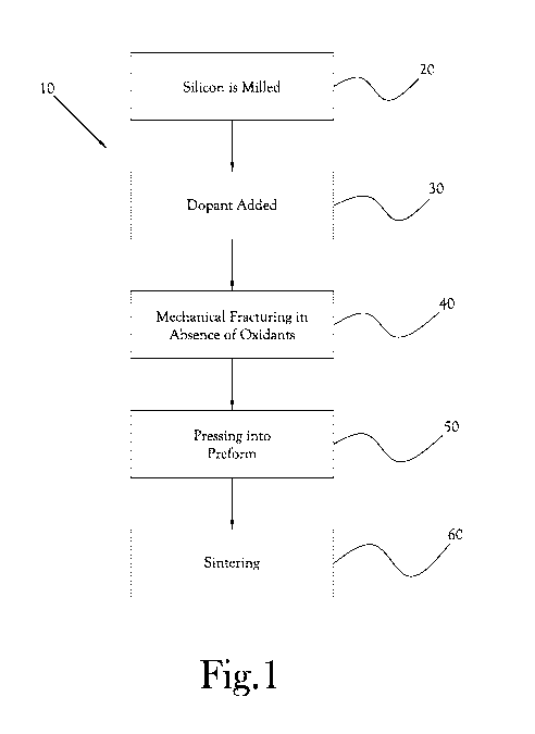
FIG. 1 is a flow diagram of an example embodiment of a method for fabricating
a
doped silicon-based thermoelectric material; and
CA 02960115 2017-03-02
WO 2016/037175
PCT/US2015/048877
FIG. 2 is a sectional view of an example embodiment of a silicon-based
thermoelectric device in which several layers of doped silicon-based
thermoelectric material
are combined.
DETAILED DESCRIPTION OF THE INVENTION
[0049] Disclosed herein are methods and processes to fabricate
thermoelectric
materials and more particularly to methods and processes to fabricate doped
silicon-based
semiconductive materials to use as thermoelectrics in the production of
electricity from
recovered waste heat. In some example embodiments, the present invention
comprises a
thermoelectric material that incorporates a silicon-based semiconductor
material.
[0050] Also disclosed herein are methods and processes that encompass the
use a
high-purity, properly-doped, nanostructured, porous silicon milled to a
particle size less than
a few microns, and sinter into a thick structure that will achieve a very high
efficiency
converting heat to electricity.
[0051] In various example embodiments of the present general inventive
concept,
fabrication of effective silicon-based thermoelectric devices involves: doping
for high
electrical conductivity for both P and N type by doping from column III and
column V of the
periodic chart respectively, as is done for semiconductor applications; doping
within the
discipline of otherwise very high purity to maintain high values for the
Seebeck Coefficient;
utilizing the ability to manipulate silicon at very high temperatures; and
reducing the thermal
conductivity by exploiting the quantum size effect for blocking phonons while
maintaining
high electrical conductivity.
[0052] The present general inventive concept, in various embodiments,
accomplishes
all of this with a porous silicon structure constructed with nano-sized grains
which are
constructed with electronic grade silicon, pre-doped to desired high
electrical conductivity
and then mechanically fractured in a controlled process to preclude oxidation
and
contamination and then recombined in a porous structure by pressing these nano
grains into a
preform and sintering at a temperature below the melting point of bulk silicon
but above the
CA 02960115 2017-03-02
WO 2016/037175
PCT/US2015/048877
11
temperature where the glassy state evolves and surface melting causes a fusion
or melting
together, in effect fusing or bonding the crystalline structures together.
[0053] Examples of the present general inventive concept encompass
approaches that
provide high operating temperature, long term temperature stability, required
low costs,
available materials, thick cross section to support large AT (i.e., difference
between
maximum and minimum temperatures associated with a temperature gradient, low
coefficient
of thermal expansion (CTE) to support the large AT, high Seebeck Coefficient,
and low
thermal conductivity.
[0054] It is desirable to have a thermoelectric material with low thermal
conductivity,
high electrical conductivity, and high Seebeck Coefficient. Through methods
and processes
according to the present general inventive concept, it is further possible to
produce
thermoelectric materials with high temperature operating capability (i.e., a
sustainable
temperature difference across its structure or AT capability) with a very low
coefficient of
thermal expansion (CTE).
[0055] A prerequisite to exploiting a thermoelectric material high
temperature
capability and its ZT is it must be able to also mechanically withstand a
large, mostly unaided
AT in service. This in turn results in a need for the Thermoelectric material
to have a
minimum CTE and maximum tensile strength (STen), and those are particularly
crucial to
minimize thermal shock susceptibility given Thermoelectric materials have a
desirably low
(which compromises that same susceptibility).
[0056] A larger thermoelectric material component or "leg" will promote the
ability to
achieve a larger unaided AT (requiring it does not mechanically fail due to
low strength and
high CTE); this is an important issue for achieving cold temperatures too.
Later we will
address the potential to refine this equation by adding to the denominator
dimensions that will
portray the thermal gradient of the system.
[0057] Generally, in many example embodiments of the present general
inventive
concept, it is desirable for a Seebeck or Peltier device to exhibit the
following characteristics:
a minimum efficiency of 15% is required for a AT of 673 K (400 C), meaning an
operating
CA 02960115 2017-03-02
WO 2016/037175
PCT/US2015/048877
12
temperature of at least 773 K (500C); a limit with regard to CTE of about 6 x
10-6/ C (or 6
ppm/ C); a Seebeck Coefficient of 220 p.V/K, which when squared is
0.0000000484 V2/K2;
electrical conductivity of at least 30,000 Siemens (which adjusts the previous
value up to
0.001452 5V2/K2); and at minimum a ZT of 1, and preferably at least 1.0164.
[0058] Silicon has a very low CTE, a high Seebeck Coefficient, and the
ability to be
tailored for specific semiconductor and electrical and thermoelectric
properties. Silicon-
based devices can be economically manufactured in large volumes from abundant
materials,
and they can be made at required very high purity levels economically. Silicon
can be
engineered into systems that can operate at high temperatures. The key issues
for success for
silicon in this most valuable application is its high thermal conductivity of
149 W/mK.
[0059] Proper nano structuring can provide a means to tailor silicon
structures for
exceptionally low thermal conductivity, as low as 0.4 W/mK, a 350 times
reduction in this
denominator in the thermo electric power factor equation which has, until now,
disqualified
silicon in this application.
[0060] Examples of the present general inventive concept encompass
approaches for
making thermoelectric devices that include a way to obtain porous, nano-sized,
equiaxed
silicon grains that could be formed into robust large shapes with large cross
sections and a
nano structured morphology, so to achieve or promote a low CTE, a low value
for thermal
conductivity, very high values for electrical conductivity, high S values, and
high operating
temperature capability.
[0061] Generally speaking, various example embodiments of the present
general
inventive concept involve the use of phonon interference to decouple the
phonon of the
thermoelectric material from the electron flow within said same thermoelectric
material. In
various example embodiments, this process includes: economically milling
silicon to nano-
sized equiaxed grains without substantial contamination; doping the silicon
grains with
boron, phosphorus, or similar materials, thereby creating a doped material
with high electrical
conductivity without increasing thermal conductivity; sintering the doped
material,
meanwhile protecting the nano-sized equiaxed grains of silicon from oxidation
between the
CA 02960115 2017-03-02
WO 2016/037175
PCT/US2015/048877
13
milling step and the sintering step; and forming the thermoelectric material
into porous,
strong, large, complex shapes, generally exhibiting high ZT.
[0062] By doping finely milled silicon with materials such as boron,
phosphorous and
arsenic among many others, it is possible to dramatically increase the
electrical conductivity
of the resulting doped thermoelectric material, while at the same time
reducing and managing
the thermal conductivity of the material. In this case, the phonon is not able
to efficiently
pass through the barrier at the interface, while the electron passes with
little or no resistance
or interference. This permits doping of the silicon to increase electrical
conductivity without
increasing the thermal conductivity, essentially decoupling of the duality of
the electron and
phonon terms. This decoupling is a quantum size effect.
[0063] In various example embodiments, methods and processes according to
the
present general inventive concept involve processing suitable silicon
precursors into nano
sized grains, essentially equiaxed, which can be formed into large net shape
simple or
complex thick shapes and sintered into structures containing these nano
structured
morphologies while containing dopants, for instance boron, that provide high
electrical
conductivity and a high Seebeck Coefficient in such a way as to preserve high
carrier
concentrations and long carrier lifetime. An element for success is protecting
the silicon
surfaces before and during sintering from any oxidation as a small amount of
oxidation in
these very small grain boundaries can cause very large increases in electrical
resistivity.
[0064] Small nano structure morphology in silicon, where the interfaces are
in the
range of a few to tens of nm, between small structures of milled silicon
grains (e.g., wires,
micropores, MEMs structures) have phonon interference at the grain boundaries
without
interference with electrical conduction. This permits lowering silicon's
otherwise high
thermal conductivity without concomitantly reducing its electrical
conductivity.
Simultaneously, doping with boron promotes high electrical conductivity. It is
also possible
to prepare silicon alloyed with other materials, for instance germanium
(typically in the range
of 20% germanium and 80% silicon) which aids milling by increasing
brittleness, and makes
a porous structure of alloyed and doped silicon alloyed with germanium, thus
increasing
temperature operating range and increasing the power factor.
CA 02960115 2017-03-02
WO 2016/037175
PCT/US2015/048877
14
[0065] Some example embodiments of the present general inventive concept
include
sintering the particles in a manner much like the process for making rebonded
fused silica. In
the case of fusing ground particles of fused silica, relatively pure glass
sand (Fe about 350
ppm, total 350 ppm impurities) is heated in the presence of oxygen at a
temperture in excess
of 2103 K (1830 C). It is then ground into powder, milled in water to make a
slip, slip cast or
otherwise prepared into a shape and then fired at about 1373 K (1100 C),
degrees less than
its melting point. In this process there are bonds permanently formed at the
surface interface
of the glass particles. Typical density is about 1.9 grams/cc, about 81% of
theoretical density.
[0066] The glass of course has a well characterized glass transition
profile, but the
idea of that the surface of silicon might behave as the amorphous variant, and
exhibit low
temperature glass transition temperature is a relatively new idea.
[0067] We have already milled silicon in alcohol to sizes in the range of
a D 50
between 300 nm and 12 microns and pressed these under pressure of 10 to 1000
MPa into 25
mm diameter pellets 25 mm tall and sintered these under vacuum at temperatures
between
1173 and 1673 K (900 and 1400 C). The result are very strong pellets with
exceptionally low
thermal conductivity, as low as 0.39 W/mK for the smaller D 50 and in the
range of 9 W/mK
for the larger particles.
[0068] So we can expect that the surface area contact between the
particles will be
increased by the elastic or plastic response of the silicon to the pressing
process and from the
formation of the meniscus formed between the particles through the glassy
behavior of the
surface of the silicon during the sintering process.
[0069] One of the concerns that must be addressed in the engineering
development of
the process engineering is the management of the particle size distribution of
the milled nano-
sized silicon¨with a fairly large fraction of fines below 100 nanometers and
the question
rises as to how these fines will behave.
[0070] Given the particles show morphology trending more towards equiaxed
particles than perfectly spherical particles as the D 50 descends, we believe
we will have a
contact area between the particles substantially larger than the 1/40th of the
diameter one
CA 02960115 2017-03-02
WO 2016/037175
PCT/US2015/048877
would expect in the perfect Hertzian arrangement of perfect spheres, perhaps
1/20th of the
diameter.
[0071] The electron requires a pathway of about 4-6 nm, while the phonon
requires a
pathway of about 230 to 300 nm. If we aim for a D 50 of about 400 nm to a
micron or more,
we can expect the lower end of the contact areas could be as low as 1/20th of
40 nm to about
60 nm. A contact area of 2 nm is too small and will interfere with electrical
conductivity
while 60 nm is in the sweet spot for interfering with thermal conductivity.
[0072] In this case it is expected that fines below 30 nm or so will melt
and migrate to
the contact areas between the particles through capillary forces, thereby
increasing the
footprint of the menisci between the particles. This we believe is a bit of
serendipity as we
can now include the fines in the mix without the need for expensive and
probably very
tedious particle size sieving of such small particles, since the increase in
the size of the
menisci will be much larger proportionately in the smaller menisci, where we
need larger
increase to assure electrical conductivity and smaller on the larger ones
where we have much
larger scope for increase. If this serendipity is not in play we may have to
resort to particle
size management through milling controls or sifting by various means.
[0073] We want to assure that electricity flows with minimal resistance
from grain to
grain, and we want to stay outside of the quantum size effect for the electron
in the
physicality of the structure. In this case we want to deal with classical and
well understood
electrical conductivity dynamics in the physical world, contact resistance to
be avoided and
staying in the domain of Ohms Law.
[0074] We also want to operate, as it were, outside of Ohms Law as to the
phonon, in
effect using the quantum size effect to preclude the phonon traveling from
grain to grain.
[0075] Contact resistance can be said to be a function of the contact
surface
roughness that causes submicron contacts, which are inimical to the objectives
of the present
general inventive concept. The better the surface finish the lower the contact
resistance; the
closer the contact area to the volume or cross section of the quantum size the
lower the
resistance. Resistance within a uniform cross section is proportional to its
resistivity and
CA 02960115 2017-03-02
WO 2016/037175
PCT/US2015/048877
16
length; it is inversely proportional to its cross-sectional area, which means
a small area in
contact with surface roughness can have very high resistivity.
[0076] In various example embodiments of the present general inventive
concept, the
cross-sectional area of the constituent particles is 200 to 800 nanometers,
leading to contact
areas in the range of 20 to 150 nanometers. Voltage is less than 900
microvolts, and at that
point minimal contact resistance can be achieved if the contact areas are
melted and do not
oxidize.
[0077] It is feasible to think of resistance like a kind of mechanical
friction, and a
contact with surface roughness would be good to avoid.
[0078] Many embodiments of the present general inventive concept avoid
contact
resistance due to the physical imperfections of the contact faces by
"melting," in effect
"fusing" the contact areas together, bringing crystalline silicon of each
grain into continuous
phase contact with each other.
[0079] But even in this case we must deal with the other element described
in contact
resistance, the size of the contact area and here we begin to cross the
Classical Limit as this is
best explained not just by a physical feature of the physical parts but by the
quantum size
effect. The melting of the silicon at the contact area and the sizes required
in this case are the
same for the electron for contact resistance and for quantum size effect to
block the electron,
and the same also for the phonon. When the size of the structures are of
similar or smaller
scale as the Fermi wavelength of the electron or other quanta, Ohm's law will
not apply. In
this case we experience quantum size effects through quantum confinement such
as 1D
geometries as in nanowires and open dimensions such as quantum dots. The sizes
of these as
they relate to the Fermi wavelength can provide insight into the interaction
of the quanta in
nanostructures such as we are constructing. But in this case the speed of the
quanta is of
course different in the case of the electron or photon, light or phonon, heat,
which changes
the domain of wavelength and frequency.
[0080] Turning now to the figures, Fig. 1 is a flow diagram illustrating an
example
embodiment of the present invention. A method or process 10 for fabricating a
doped
CA 02960115 2017-03-02
WO 2016/037175
PCT/US2015/048877
17
silicon-based thermoelectric material begins by milling electronic-grade
silicon into nano-
sized grains or particulates 20, which are doped 30 with a dopant to create a
material with the
desired high electrical conductivity and other desired physical properties.
The doped silicon
material is mechanically fractured 40 in a controlled process to preclude
oxidation and
contamination. The doped nano-sized grains are then pressed into a preform 50
and then
sintered 60 at a temperature below the melting point of bulk silicon but above
the temperature
where the glassy state evolves and surface melting causes a fusion or melting
together, in
effect fusing or bonding the crystalline structures together. The process or
method creates a
porous structure
[0081] In some embodiments, the addition of ceramic pellets (zirconia
pellets, for
example, but silicon nitride is preferred to minimize harmful contamination)
to the attrition
mill has been found useful in accelerating the milling 20 of the silicon
particulates.
[0082] In many embodiments, whether the final product is better suited to
act as an
N-type element or P-type element in a thermoelectric device is determined by
the specific
dopant 30 mixed with the silicon grains or particulates.
[0083] In various embodiments, a number of dopants are used to give the
final
thermoelectric material desired thermal, electrical, and mechanical
properties. In some
embodiments, dopants include one or more of the following: selenium,
tellurium, germanium,
tungsten, boron, phosphorus, and arsenic. In some embodiments, the formation
of a planar or
complexly shaped thermoelectric device includes a process in which one side is
fabricated
with silicon doped to be an N-type semiconductor and the second side is
fabricated with
silicon doped to be a P-type semiconductor. In some embodiments, a planar or
complexly
shaped thermoelectric device includes a first, thick side that is fabricated
with silicon doped
to be an N-type semiconductor and the second, thin side that is fabricated
with silicon doped
to be a P-type semiconductor. In some embodiments, a planar or complexly
shaped
thermoelectric device includes a first, thick side that is fabricated with
silicon doped to be an
P-type semiconductor and the second, thin side that is fabricated with silicon
doped to be a
N-type semiconductor. In some embodiments, the thin side of a thermoelectric
device
comprises a thin film. In some embodiments the P-type and N-type powders can
be loaded
CA 02960115 2017-03-02
WO 2016/037175
PCT/US2015/048877
18
into a dry press tool such that one side of the pressed pellet is an N-type
semiconductor and
the other is a P-type semiconductor.
[0084] For P-type semiconductor materials, the dopant often includes boron,
aluminum, gallium, or generally a Group III element, or a combination of Group
III elements.
[0085] For N-type semiconductor materials, the dopant often includes
phosphorus,
arsenic, or generally a Group V element, or a combination of Group V elements.
[0086] In several embodiments, one of the final phases of the fabrication
process
involves sintering the material into a polycrystalline form and shape with
controlled porosity
and density. The sintering process comprises a solid-state diffusional process
in which
adjacent grains and particulates bond at a homologous temperature of
approximately 1375
C. In several embodiments, a number of methods are used to shape a mixture of
milled and
doped silicon particulates into a green body for sintering. In various
embodiments, the
mixture is extruded, injection molded, die-pressed, isostatically pressed or
slip cast to
produce a green body of desired shape. Sintering of the green body is carried
out in an
atmosphere that is substantially inert, for example, argon, helium, or a
vacuum. In various
embodiments, the sintering atmosphere ranges from a substantial vacuum to
atmospheric
pressure. Sintering is carried out at a temperature ranging from 1000 C to
approximately
1414 C. Generally, sintering temperature is at least 1150 C, and in many
embodiments at
least 1250 C, to increase the rate of solid state sintering. The particular
sintering
temperature is determinable empirically and depends largely on particle size,
amount of
dopant, density of the green body, and final density desired in the sintered
thermoelectric
material, with higher final densities requiring higher sintering temperatures.
Generally, the
smaller the size of the milled silicon particulates in the green body, and the
higher its density,
the lower is the required sintering temperature. In most embodiments,
sintering is carried out
at a temperature below the melting point of silicon, in order to preserve the
reticulated
porosity of the polycrystalline structure. One must consider that the level of
doping will
affect the melting point of the silicon and thus the sintering temperature.
One of ordinary skill
in the arts addressed here will see that one wants to sinter at a temperature
below the
transition from solidus to liquidus and make a very good fused bond between
the grains.
CA 02960115 2017-03-02
WO 2016/037175
PCT/US2015/048877
19
[0087] In a thermoelectric material fabricated according to a method such
as one of
the disclosed example embodiments, the porosity of the fabricated structure is
reticulated.
When the milled and doped silicon particulates are sintered, for example as
described above,
the final polycrystalline product generally exhibits a porosity of at least
20%, and often
between 20% and 45%. In some embodiments, the final polycrystalline product
generally
exhibits a porosity of between 25% and 45%. In some embodiments, the final
polycrystalline
product generally exhibits a porosity of approximately 35%. The porosity of
the sintered
polycrystalline thermoelectric material contributes to the low density of the
material, and the
low density of the material gives the material a lower thermal conductivity
than many
competing semiconductive products. In some embodiments, the final
polycrystalline product
exhibits a thermal conductivity in the range of 0.1 to 12 Watts per meter
Kelvin. Further, it is
possible to infiltrate the porous thermoelectric structure with a variety of
materials to modify
the thermal conductivity, electrical conductivity, and Seebeck Coefficient of
the fabricated
thermoelectric structure. For example, in some embodiments, reticulated porous
spaces in
the polycrystalline thermoelectric material are infiltrated with ethyl
silicate or colloidal silica
(two example substances with low thermal conductivity and low coefficients of
thermal
expansion). In other cases it can be filled with a material which is
electrically conductive.
[0088] In several example embodiments, the final product is a silicon-based
thermoelectric material comprising a heterogeneous mixture of silicon
particulates,
substantially free of oxidants, with a dopant added to affect the
semiconductive properties of
the thermoelectric material, the heterogeneous mixture having been sintered to
form a
polycrystalline silicon-based thermoelectric material. In some example
embodiments, the
thermoelectric material includes at least two layers having different
thermoelectric properties.
[0089] In some example embodiments, a thermoelectric device comprises
multiple
layers of silicon-based thermoelectric materials, with each layer having at
least a slightly
different material composition and therefore having a different thermal
conductivity,
electrical conductivity, or Seebeck Coefficient from an adjacent layer. Fig. 2
illustrates one
example embodiment of a multi-layer thermoelectric device. As shown in Fig. 2,
a
thermoelectric device 101 comprises three layers, including a top layer 110, a
middle layer
120, and a bottom layer 130; the three layers combine to form a laminate body
with an upper
CA 02960115 2017-03-02
WO 2016/037175
PCT/US2015/048877
face 105 and a lower face 145. In the illustrated example embodiment, each of
the three
layers contains a different combination of milled silicon particulates and
dopant. In the
illustrated example embodiment, all layers contain the same dopant, but the
layers differ in
that the top layer 110 contains the lowest concentration of dopant (or,
alternatively, the
lowest amount of dopant as a weight percentage of the total heterogeneous
mixture in the top
layer 110); the middle layer 120 conatins a slightly higher concentration of
dopant than the
top layer 110; and the bottom layer contains the highest concentration of
dopant of all the
three layers. As a result of the differing concentrations of dopant, each
layer has slightly
different semiconductive and thermoelectric properties. In the illustrated
example
embodiment, the top layer 110 has less thermal and electrical conductivity
than the layers
below it. Therefore, in one use of the illustrated example embodiment
multilayer
thermoelectric device, the upper face 105 of the device 101 faces a heat
source, and the lower
face 145 of the device 101 faces the cold side of the thermal gradient; having
the top layer
110, with its relatively low thermal conductivity, facing the heat source
protects the structural
integrity of the device 101 and helps to maintain the temperature gradient
across the cross-
section of the device 101. At the same time, the other layers 120 and 130,
with their greater
electrical conductivity, are well equipped to take advantage of the electron
flow through the
top layer 110. Those of skill in the art will recognize that other uses for
multi-layer
thermoelectric devices are possible and are contemplated by the present
invention.
[0090] In some
alternative example embodiments that comprise thermoelectric device
with multiple layers of polycrystalline silicon-based thermoelectric
materials, the layers differ
in that each layer comprises a different dopant or a different combination or
ratio of dopants.
For example, in an example embodiment, a three-layer thermoelectric device
includes one
layer in which the principal dopant includes selenium; one layer in which the
principal dopant
includes tellurium; and one layer in which the principal dopant includes
tungsten. As a result
of the dopant differences, each layer has different semiconductive and
thermoelectric
properties.
[0091] In some
alternative example embodiments that comprise thermoelectric device
with multiple layers of polycrystalline silicon-based thermoelectric
materials, the layers differ
in that the density of each layer is different from the density of other
layers in the device. As
CA 02960115 2017-03-02
WO 2016/037175
PCT/US2015/048877
21
a result of the density differences, each layer has different semiconductive
and thermoelectric
properties.
[0092] In some of the several embodiments, the present invention allows for
the
fabrication of planar, net-shaped, or complexly shaped thermoelectric devices
that are
capable of being installed in a variety of places, and in particular are
capable of being
installed in places to absorb waste heat from machinery or equipment and
transform the waste
heat into electricity. For example, thermoelectric devices according to some
of the example
embodiments of the present invention are capable of being wrapped around pipes
in some
industrial settings, absorbing heat from the pipe.
[0093] The methods and processes disclosed above are useful for producing
highly
efficient silicon-based thermoelectric materials that have high Seebeck
Coefficients, high
electrical conductivity, and low thermal conductivity, with the precise
parameters of each
silicon-based thermoelectric material dependent upon the nature of the dopant,
the particle
size of the milled silicon particulates, and the density of the final sintered
polycrystalline
thermoelectric material. Such thermoelectric materials are susceptible to
being worked to
construct planar and complex net-shaped objects that can be fitted into
locations where they
may be used to recover waste heat. Such thermoelectric materials have cross
sections with
properties to maintain an adequate temperature differential between the two
opposing sides in
order to generate voltage efficiently. These silicon-based thermoelectric
materials generally
have larger cross sections than many competing thermoelectric and
semiconductor materials.
The larger cross section of such silicon-based thermoelectric materials is
useful for
maintaining a temperature gradient. Doped silicon-based thermoelectric
material have high
tensile strength, have resistance to thermal shock, and are formable into
layers and curved
and other shapes to allow the creation of graded indices for electrical,
thermal, or other
parameters. These silicon-based thermoelectric materials are useful in a
number of contexts,
and it is feasible to use them to efficiently recover heat over a large range
of temperatures. In
some embodiments, silicon-based thermoelectric materials are able to
efficiently recover heat
within a range of -65 C to 1100 C.
CA 02960115 2017-03-02
WO 2016/037175
PCT/US2015/048877
22
[0094] Moreover, while the example embodiments described above have
generally
involved silicon grains or particulates doped with another material, it is not
the intention of
the present application to limit the general inventive concept to silicon-
based materials. A
number of semiconductor materials are encompassed by the present general
inventive
concept, including, without limitation: germanium, diamond, silicon carbide,
silicon
germanium; gallium arsenide, gallium nitride, aluminum arsenide, aluminum
phosphide;
tetrahedrites, bismuth telluride, skutterudites.
[0095] As with silicon-based doped thermoelectric materials, other doped
thermoelectric materials often employ one or more specific dopants to achieve
desired
electrical, thermal, or mechanical properties, including specific dopants to
create N-type and
P-type semiconductors. Thus, for example, for gallium arsenide, N-type dopants
include
tellurium, sulphur (substituting As), tin, silicon, germanium (substituting
Ga); and P-type
dopants include zinc, chromium (substituting Ga), silicon, germanium
(substituting As). For
gallium phosphide, N-type dopants include tellurium, selenium, sulphur
(substituting
phosphorus); and P-type dopants include zinc, magnesium (substituting Ga), tin
(substituting
P). For cadmium telluride, N-type dopants include indium, aluminum
(substituting Cd),
chlorine (substituting Te); and P-type dopants include phosphorus
(substituting Te), lithium,
sodium (substituting Cd). For cadmium sulfide, N-type dopants include gallium
(substituting
Cd), iodine, fluorine (substituting S); and P-type dopants include lithium,
sodium
(substituting Cd).
[0096] As a general matter, for a number of semiconductor materials, N-type
dopants
include phosphorus, arsenic, antimony, bismuth, and lithium. Phosphorus
diffuses quickly,
so is usually used for bulk doping, or for well formation. Used in solar
cells. Can be added by
diffusion of phosphine gas. Bulk doping can be achieved by nuclear
transmutation, by
irradiation of pure silicon with neutrons in a nuclear reactor. Phosphorus
also traps gold
atoms, which otherwise quickly diffuse through silicon and act as
recombination centers.
Arsenic's slower diffusion allows using it for diffused junctions. Used for
buried layers. Has
similar atomic radius to silicon, high concentrations can be achieved. Its
diffusivity is about a
tenth of phosphorus or boron, so is used where the dopant should stay in place
during
subsequent thermal processing. Useful for shallow diffusions where well-
controlled abrupt
CA 02960115 2017-03-02
WO 2016/037175
PCT/US2015/048877
23
boundary is desired. Preferred dopant in VLSI circuits. Preferred dopant in
low resistivity
ranges. Antimony is a n-type dopant. It has a small diffusion coefficient.
Used for buried
layers. Has diffusivity similar to arsenic, is used as its alternative. Its
diffusion is virtually
purely substitutional, with no interstitials, so it is free of anomalous
effects. For this superior
property, it is sometimes used in VLSI instead of arsenic. Heavy doping with
antimony is
important for power devices. Heavily antimony-doped silicon has lower
concentration of
oxygen impurities; minimal autodoping effects make it suitable for epitaxial
substrates.
Bismuth is a dopant for long-wavelength infrared photoconduction silicon
detectors, a viable
n-type alternative to the p-type gallium-doped material. Lithium is used for
doping silicon
for radiation hardened solar cells. The lithium presence anneals defects in
the lattice produced
by protons and neutrons. Lithium can be introduced to boron-doped p+ silicon,
in amounts
low enough to maintain the p character of the material, or in large enough
amount to
counterdope it to low-resistivity n type.
[0097] As a general matter, for a number of semiconductor materials, P-type
dopants
include boron, aluminum, nitrogen, gallium, and indium. Boron's diffusion rate
allows easy
control of junction depths, and boron can be added by diffusion of diborane
gas. As a rule, it
is the only acceptor with sufficient solubility for efficient emitters in
transistors and other
applications requiring extremely high dopant concentrations. It diffuses about
as fast as
phosphorus. Aluminum is used for deep P-diffusions (and is also a common
unintentional
impurity). Nitrogen is important for growing defect-free silicon crystal; it
improves
mechanical strength of the lattice, increases bulk microdefect generation,
suppresses vacancy
agglomeration. Gallium is a dopant used for long-wavelength infrared
photoconduction
silicon detectors in the 8-14 um atmospheric window. Gallium-doped silicon is
also
promising for solar cells, due to its long minority carrier lifetime with no
lifetime
degradation; as such it is gaining importance as a replacement of boron doped
substrates for
solar cell applications. Indium is a dopant used for long-wavelength infrared
photoconduction silicon detectors in the 3-5 um atmospheric window.
[0098] As a general matter, for the Group III-V semiconductors, selenium,
tellurium,
silicon and germanium are common N-type dopants, and beryllium, zinc, silicon
and
germanium cadmium are common P-type dopants.
CA 02960115 2017-03-02
WO 2016/037175
PCT/US2015/048877
24
[0099] Moreover, as a general matter, dopants that are used in various
embodiments of the
present general inventive concept include germanium, silicon, xenon, gold, and
platinum.
[00100] Thermoelectric materials fabricated according to some of the
several
embodiments of the present general inventive concept maintain good Seebeck
Coefficient
while getting high values for electrical conductivity. In some embodiments,
employing larger
atoms for doping, such as arsenic, particularly on the N leg, allows less
mobility within the
material and enhances the usefulness of the material in high temperature
operations.
Additionally, in some embodiments, larger legs can take advantage of space,
time and
velocity to realize more efficient operation and higher unaided Delta T. The
advantages of
some example materials according to the present general inventive concept, as
over selected
semiconductor materials of the prior art, are summarized in Table 1.
CA 02960115 2017-03-02
WO 2016/037175 PCT/US2015/048877
Table 1
Operating Seebeck Seebeck Elec. Elec.
CTE Temp. (mV) (mV) (Siemens)
(Siemens)
Material (ppm) (Kelvins) (lower) (upper) (lower) (upper)
Bi2Te3 & family 18 550 0.00008 0.00014 50000 80000
Oxides 8 900 0.00008 0.00012 12000 18000
Lead Telluride 16 400 0.00014 0.00018 20000 30000
Half Heusler 16 600 0.00012 0.00018 40000 80000
Skutterudites 16 750 0.00012 0.00018 40000 80000
ZNTL 12 700 0.00012 0.00018 40000 80000
LAST 14 700 0.00014 0.00018 20000 30000
Magnesium Silicide 11.5 700 240 300 6000 32000
CA 02960115 2017-03-02
WO 2016/037175 PCT/US2015/048877
26
Table 1 (Continued)
Thermal Thermal Rare
(W/mK) (W/mK) ZT ZT Earth / Temp. Large
Material (upper) (lower) (lower) (upper) Precious? Cost Stable? X-Section?
Bi2Te3
& family 2.5 1.5 0.0704 0.57493 Yes High
No <1 mm
Oxides 3 2 0.02304 0.11664 ? High
Yes <1 mm
Lead Telluride 3 1.5 0.05227 0.2592 Yes High
No <1 mm
Half Heusler 2.5 1.5 0.13824 1.0368 Yes High
No <1 mm
Skutterudites 10 1.5 0.0432 1.296 Yes High No <1
mm
ZNTL 2.5 1.5 0.16128 1.2096 Yes High
no <1 mm
LAST 0.8 0.5 0.343 1.3608 Yes High
No <1 mm
Mg. Silicide 6 3.6 0.3 0.8 No Mod. No Thin
CA 02960115 2017-03-02
WO 2016/037175 PCT/US2015/048877
27
Table 1 (Continued)
Operating Seebeck Seebeck Elec. Elec.
CTE Temp. (mV) (mV)
(Siemens) (Siemens)
Material (ppm) (Kelvins) (lower) (upper) (lower) (upper)
Micro Channels 3.6 900 0.00012 0.00018 25000
35000
Nano Fiber 3.6 900 0.00012 0.00018 25000
35000
Silicon Germanium 4 1400 0.00014 0.00028 20000
40000
Porous Silicon 3.6 1400 0.00017 0.00024 25000
50000
Table 1 (Continued)
Thermal Thermal Rare
(W/mK) (W/mK) ZT ZT Earth / Temp.
Large
Material (upper) (lower) (lower) (upper) Precious? Cost Stable? X-Section?
Micro
Channels 1.5 0.6 0.216 1.701 No High Yes
<1 mm
Nano Fiber 1.5 0.6 0.216 1.701 No High Yes
<1 mm
Si Germanium 60 2.5 0.00915 1.75616 Yes (Ge) High Yes 10 +
Porous Silicon 1 0.6 1.0115 6.72 No Low Yes
25+
[00101] In some embodiments, silicon-based thermoelectric materials
fabricated
according to some of the several embodiments of the present general inventive
concept
CA 02960115 2017-03-02
WO 2016/037175
PCT/US2015/048877
28
provide increased Seebeck Coefficient, high electrical conductivity and low
thermal
conductivity. Silicon has the advantage of a low CTE (less than 4 ppm) and low
cost.
Silicon pellets can be made economically in large cross sections, supporting
large unaided
Delta T. Industrial milling facilitates the fabrication of porous structures
instead of bulk hot
pressed structures, thus providing a finished product with a lower thermal
conductivity.
[00102] Further, in several example embodiments, the use of nano-
structuring allows
practitioners to obtain very low thermal conductivity in the finished product.
The
construction of a porous nano-structure of oxygen-free doped silicon also
provides for a
material with low thermal conductivity. Doping the material with boron adds
low electrical
resistivity. The result is a thermoelectric material with a high Seebeck
Coefficient, optimized
electrical conductivity, and low thermal conductivity. In some embodiments, it
is possible to
engineer a material with thermal conductivity of less than 1 W/MK using
nanostructures. It
is further possible to dope for low electrical resistivity, using boron for
example. In some
embodiments, the material is "overdoped" with boron to achieve desired
properties. In some
embodiments, the doping also includes such materials as phosphorous or
arsenic.
[00103] Smaller particles will of course suffer stresses farther below the
limits of the
modulus as a function of their size, so smaller size is preferable for
enduring many cycles
without mechanical failure. It is a feature in the present design that very
small particles are
bonded together below the melting point of silicon and that the smaller
particles will impart a
smaller stress on those bonded joints.
[00104] In this case the fact of an ability to create a large economical
throughput of
nano-sized slightly angular silicon also provides the ability to make desired
large shapes in
porous silicon is in contrast to all the prior art listed above which lacks
the ability to make
large economical strong form factors.
[00105] The best source of silicon for this application is a very pure
silicon
manufactured from the "Siemens" process. In this case, metallurgical silicon
is processed into
a chemical precursor so that it can be purified by distillation before
deposition into an ingot
or boulle through CVD. This material can be "doped" with elements, for
instance from
column III of the periodic chart, for example boron, or column V, for example
phosphorous
CA 02960115 2017-03-02
WO 2016/037175
PCT/US2015/048877
29
and arsenic are common. In this way electrical conductivity and other
semiconductor
behaviors can be tailored. However, one with ordinary skill in the art will
understand and
anticipate that our approach can be applied to a large list of thermoelectric
materials. Namely
that nano sizing in our milling and pressing and sintering as described herein
will provide
large benefits to all thermoelectric materials.
[00106] It is important to note that there is a well-studied quantum size
effect being
considered in the realm of thermoelectric devices wherein it is now understood
that a
structure where the contacts paths with dimensions less than 5 nanometers will
not conduct
electricity very well and less than 200 nanometers will not conduct phonons
very well.
Therefor when making a porous nanostructure, if one desires high electrical
conductivity in
the silicon structure itself, one will tailor the starting grains pressed into
the preforms to avoid
creating contact points less than five nanometers, or make other arrangements
for electrical
conductivity, for example through addition of graphite, silicon carbide or
other complex
matrix constituents.
[00107] Silicon has a well-known "glassy state" far below the melting
point, which is
designated by most resources at 1414 to 1417 degrees centigrade. It is
questionable if the
actual melting point of silicon is known since most all evaluations are done
in quartz
crucibles which bring oxygen into the melt in the form of silicon monoxide.
For instance
clean un-oxidized nano particles of silicon, usually cleaned of the oxide mono
native layer
with hydrogen fluoride, has been reported to melt at temperatures well below
one thousand
degrees centigrade.
[00108] The surface chemistry of silicon has long been recognized for
having a glassy
state, and speculation as to its nature often includes reference to the
"native oxide" layer
normally found on the surface of silicon. Andy Grove while at Fairchild
performed and
reported some of the seminal work in this regard with respect to semiconductor
device design
and processing.
[00109] One of the long unmet needs with regard to nano-sized or even
micron sized
silicon is a safe inexpensive process for taking silicon grains of a larger
size, one to several
CA 02960115 2017-03-02
WO 2016/037175
PCT/US2015/048877
mm or larger, and diminishing the size to microns or nanometers free of
oxidation, which
means maintaining its reactivity and making the downsizing safe.
[00110] If we assume a perfect Hertzian contact area between two equally-
sized
spheres we might expect a contact area of 1/40th of the diameter. In such a
case we would
want a maximum of perhaps 150 nm to preclude phonon transmission, and a
minimum of
about 5 pm to ensure electron transmission. To achieve this we would want a
particle size
distribution of the grains to be pressed to cut off at about 3 p.m, so as to
limit the largest
contact areas to about a hundred nm.
[00111] It is possible to sinter at relatively low temperatures, perhaps
not 1623 K
(1350 C) but as low as 1173 K (700 C). However, the higher temperature in
fused silica
results in a higher STens, because of the larger meniscus formed. One can
expect that the
same phenomena will be in play with the sintered porous rebonded silicon, so
the higher
temperature may still be desired.
[00112] While the surfaces of our particles are probably elongated semi
elipsoid
shapes, and irregular, our SEM and micrograph work shows they increasingly
equiaxed as
they are milled to D 50 size in the several hundred nanometer size. We can
expect surfaces
with some irregularities. However, these defects will be exceptionally small
and we can
expect that the glassy formation of the meniscus will cure these defects and
create a larger
more perfect bond between the materials. We will be pressing the powder
extracted from the
slurry with some great pressure, and this will cause deformation and increase
the contact area.
[00113] At the same time as we will be sintering in the range of 1173 -
1623 K (900 to
1350 C). In this range we can expect to form the "glassy" state of the surface
of the silicon,
which in the vacuum will result in the contact area collecting a mass and
resulting in a
meniscus increasing the contact area. According to the reports by the
investigators at
Innovalight, we can expect the smallest particles to be absorbed in the glass
state. The size of
the meniscus will be a function of the surface area, viscosity, surface energy
and temperature
of course. So this means that we can expect that the surface area will
increase in this respect.
CA 02960115 2017-03-02
WO 2016/037175
PCT/US2015/048877
31
[00114] In this case we can expect that we will be able to mill silicon to
a D 50 of one
micron or less, press it into a large pellet, perhaps 25 mm diameter and 25 mm
thick, sinter it
in a vacuum of about 0.2 microns in the range of 1173 and 1673 K (900 to 1400
C) and have
contact areas between the milled grains larger than 5 nm and smaller than 200
nm, resulting
in thermal conductivity in the range of 0.5 W/mK and very low stresses on the
meniscus as
the structure expands and contracts in each cycle.
[00115] This silicon is milled in a protected cover to preclude oxygen.
Ethanol is a
preferred cover since it protects from oxygen and can be economically
recycled.
[00116] In the case of the silicon, it can be doped with materials from
column III or V,
such as boron, phosphorous, arsenic and others to electrical conductivity as
high as 109,000
Siemens, as can be silicon carbide.
[00117] Silica (5i02) and graphite (C) can also be added as sintering aids
to provide a
stronger bonding among the nano particles in the sintering process. In terms
of adding
sintering aids to create other phases in the physical matrix, the family of
oxides, nitrides and
carbides are well known to one skilled in the ceramic fabrication arts. For
instance, yttrium
oxide, aluminum oxide, silicon oxide, and zirconium oxide are all well-known
sintering aids
in the fabrication of silicon nitride, which can be of value in this approach.
The object of this
teaching is to give examples of a novel way of adding proscribed amounts of
sintering aids to
the milling of the silicon at some point to create the desired precursors for
fabrication of
structures in the matrix of value to the objects of the present general
inventive concept.
[00118] Once the material(s) are properly milled such that about 95% of the
particles
are below a minimum, 800 nanometers has been achieved and is suggested as
optimal, they
must be formed into a preform, but optimally without a binder.
[00119] In such a case applying a lubricant, ethanol is again considered
ideal among
others as practioners in the operation of vacuum furnaces are comfortable
evacuating ethanol,
to the powders in a pressing tool will enable the powders to organize
themselves under
pressure into a structure that will retain significant binderless preform
structure. Pressing
should be done at 100-900 MPa, and it is suggested that about 450-750 MPa is
optimal. It is
CA 02960115 2017-03-02
WO 2016/037175
PCT/US2015/048877
32
suggested that a tapered die will provide the best process efficiency and
yield for exit of the
pressed preform in the absence of binders or other lubricants.
[00120] Once these preforms are completed and ready to sintered it is best
that the
object is then sintered in a vacuum furnace. Optimally argon is back filled
and evacuated one
or more times to remove oxygen from the atmosphere, and oxygen liberated at
various
temperatures from constituents in the furnace. Temperatures of 300 and 700
degrees Celsius
are suggested as good points for purging with argon and returning to the
suggested vacuum at
the level of 0.2 microns, or minus 5 or 6 torr. The sintering temperature will
depend upon a
number of factors, including the mix of carbon, silica, silicon and silicon
carbide. One would
find that 950 to 1400 Celsius will provide the range of temperature required.
[00121] In some embodiments of the present general inventive concept, a
process for
fabricating a doped thermoelectric material encompasses mixing particulates of
a
semiconductor base material with a dopant; milling the semiconductor base
material
particulates containing the dopant so that said particulates have a median
size of less than
3,000 nanometers and are substantially equiaxed; and sintering said
particulates containing
the dopant in an atmosphere essentially free of oxygen to form a doped
thermoelectric
material.
[00122] In some embodiments, said semiconductor base material includes a
material
selected from the group consisting of silicon, germanium, diamond, silicon
carbide, silicon
germanium, gallium arsenide, gallium nitride, gallium phosphide, aluminum
arsenide,
aluminum phosphide, cadmium telluride, cadmium sulfide, bismuth telluride,
tetrahedrites,
and skutterudites.
[00123] In some embodiments, said thermoelectric material is a P-type
semiconductor
and said dopant includes boron, aluminum, gallium, or a similar P-type dopant.
[00124] In some embodiments, said thermoelectric material is an N-type
semiconductor and said dopant includes phosphorus, arsenic, or a similar N-
type dopant.
CA 02960115 2017-03-02
WO 2016/037175
PCT/US2015/048877
33
[00125] In some embodiments, said dopant includes germanium or a similar
material
to improve the thermal, electrical, or mechanical properties of the
thermoelectric material.
[00126] In some embodiments, said dopant includes an element selected from
the
group consisting of selenium, tellurium, germanium, tungsten, boron,
phosphorus, and
arsenic.
[00127] In some embodiments, said sintering is carried out in an inert
atmosphere.
[00128] In some embodiments, said sintering is carried out under reduced
pressure.
[00129] In some embodiments, said sintering is carried out at a temperature
of between
1000 degrees Celsius and 1414 degrees Celsius.
[00130] In some embodiments of the present general inventive concept, a
doped
silicon-based thermoelectric material includes milled silicon grain particles
having a median
particle size of less than 3,000 nanometers, said milled silicon particles
being substantially
equiaxed, and a dopant mixed with milled silicon particles to form a doped
silicon-containing
material, said dopant reducing the thermal conductivity of the doped silicon-
containing
material compared to the milled silicon grain particles, said doped silicon-
containing material
being sintered in the absence of oxidants to form a doped silicon-based
thermoelectric
material.
[00131] In some embodiments, said doped silicon-based thermoelectric
material is a P-
type semiconductor and said dopant includes boron, aluminum, gallium, or a
similar P-type
dopant.
[00132] In some embodiments, said doped silicon-based thermoelectric
material is an
N-type semiconductor and said dopant includes phosphorus, arsenic, or a
similar N-type
dopant.
CA 02960115 2017-03-02
WO 2016/037175
PCT/US2015/048877
34
[00133] In some embodiments, said dopant includes germanium or a similar
material
to improve the thermal, electrical, or mechanical properties of the doped
silicon-based
thermoelectric material.
[00134] In some embodiments, said sintering is carried out under reduced
pressure.
[00135] In some embodiments, a method for fabricating a doped silicon-based
thermoelectric material includes introducing a first quantity of silicon
particulates into an
attrition mill in the absence of oxidants, admixing the first quantity of
silicon particulates
with a dopant to affect the semiconductive properties of the thermoelectric
material,
subjecting said first quantity of silicon particulates combined with dopant to
attrition in the
attrition mill for a time sufficient to reduce at least a portion of said
silicon particulates to a
preselected average particle size to produce a second quantity of reduced
particle size doped
silicon particulates being essentially oxidant free, said second quantity of
reduced particle
size doped silicon particulates having a median size of less than 3,000
nanometers, said
second quantity of reduced particle size doped silicon particulates having
substantially
equiaxed grain particles, withdrawing from said attrition mill at least a
portion of said second
quantity of reduced particle size doped silicon particulates, fracturing the
doped silicon
particulates in the absence of oxidants; pressing the doped silicon
particulates into a preform;
and sintering doped silicon particulates in the absence of oxidants to form a
doped silicon-
based thermoelectric material.
[00136] In some embodiments, said doped silicon-based thermoelectric
material is a P-
type semiconductor and said dopant includes boron, aluminum, gallium, or a
similar P-type
dopant.
[00137] In some embodiments, said doped silicon-based thermoelectric
material is an
N-type semiconductor and said dopant includes phosphorus, arsenic, or a
similar N-type
dopant.
CA 02960115 2017-03-02
WO 2016/037175
PCT/US2015/048877
[00138] In some embodiments, said dopant includes germanium or a similar
material
to improve the thermal, electrical, or mechanical properties of the doped
silicon-based
thermoelectric material.
[00139] In some embodiments, said dopant includes an element selected from
the
group consisting of selenium, tellurium, germanium, tungsten, boron,
phosphorus, and
arsenic.In some embodiments, said sintering is carried out under reduced
pressure.
[00140] While the present invention has been illustrated by description of
several
embodiments and while the illustrative embodiments have been described in
considerable
detail, it is not the intention of the applicant to restrict or in any way
limit the scope of the
appended claims to such detail. Additional advantages and modifications will
readily appear
to those skilled in the art. The invention in its broader aspects is therefore
not limited to the
specific details, representative apparatus and methods, and illustrative
examples shown and
described. Accordingly, departures may be made from such details without
departing from
the spirit or scope of applicant's general inventive concept.