Note: Descriptions are shown in the official language in which they were submitted.
CA 02960991 2017-03-10
PATENT APPLICATION
VERY LOW INDUCTANCE FLEXIBLE ELECTRICAL CONNECTOR INSERT
CROSS-REFERENCE TO RELATED APPLICATIONS
[0001] This application claims priority to and the benefit of the
filing of U.S.
Provisional Patent Application Serial No. 61/898,927, entitled "Very Low
Inductance Design
for Electrical Connector Insert", filed on November 1, 2013.
STATEMENT REGARDING FEDERALLY SPONSORED RESEARCH OR
DEVELOPMENT
[0002] Not Applicable.
INCORPORATION BY REFERENCE OF MATERIAL SUBMITTED ON A COMPACT DISC
[0003] Not Applicable.
COPYRIGHTED MATERIAL
[0004] Not Applicable.
BACKGROUND OF THE INVENTION
Field of the Invention (Technical Field):
[0005] The present invention relates to inserts installed into an
existing or new
electrical connector to reliably add electrical circuitry to the system and
concomitant
methods of use and construction.
Description of Related Art:
[0006] The present invention primarily relates to an insert installed
into an existing
or new electrical connector to reliably add electrical circuitry to the
system. Current
-2-
technology in this field uses either standard circuit board technology or
EESeal silicone
inserts. The circuit board technology corrupts the existing environmental seal
of the
connector, and so is unsuitable for high-reliability connectors. The EESeal
technology is
made primarily from silicone elastomer, and so does not corrupt the existing
seal.
However, the filament wire interconnects within the insert introduce unwanted
stray
inductance and are labor intensive to construct. The additional stray
inductance limits
EESeal effectiveness at frequencies above 100 MHz. Both technologies
incorporate
discrete surface mount devices, primarily capacitors, whose stray inductance
is typically a
minimum of 0.5nH. The stray inductance of the surface mount devices also
limits high
frequency performance.
BRIEF SUMMARY OF THE INVENTION
[0007] The present invention is of a connector insert comprising one or
more layers
of conductive elastomer. Preferably, the layers have a volume resistivity less
than about
0.010 ohms-cm. The insert can be placeable into an existing connector. The
layers have
holes for pins of the connector, and provide at least a connector shell
contact, a ground
plane, and a pin contact. The connector insert can additionally comprise a
capacitor,
preferably comprising a plurality of layers of conductive elastomer, with
separation
provided by at least one layer of non-conductive material, and most preferably
wherein the
at least one layer of non-conductive material comprises non-conductive
elastomer. The
insert may additionally comprise one or more other electrical components, and
one or more
electrical components may comprise elastomer.
[0008] The invention is additionally of a concomitant method of employing a
connector insert, the method comprising the steps of: fabricating one or more
layers of
conductive elastomer as an insert; and placing the insert into a connector.
The layers
preferably have a volume resistivity less than about 0.010 ohms-cm. The
connector may
be an existing connector. Holes are formed in the insert for the pins of the
connector, and
the insert provides at least a connector shell contact, a ground plane, and a
pin contact for
the connector. A capacitor may be formed in the insert, preferably wherein the
capacitor
comprises a plurality of layers of conductive elastomer, with separation
provided by at least
one layer of non-conductive material, and most preferably wherein the at least
one layer of
non-conductive material comprises non-conductive elastomer. One or more
electrical
CA 2960991 2019-10-28
CA 02960991 2017-03-10
-3-
components may be formed in the insert, and one or more of the electrical
components
may comprise elastomer.
[0009] The invention is further of a capacitor for a connector insert,
the capacitor
comprising a plurality of layers of elastomer, with separation provided by at
least one layer
of non-conductive material.
[0010] Further scope of applicability of the present invention will be
set forth in part
in the detailed description to follow, taken in conjunction with the
accompanying drawings,
and in part will become apparent to those skilled in the art upon examination
of the
following, or may be learned by practice of the invention. The objects and
advantages of
the invention may be realized and attained by means of the instrumentalities
and
combinations particularly pointed out in the appended claims.
BRIEF DESCRIPTION OF THE SEVERAL VIEWS OF THE DRAWINGS
[0011] The accompanying drawings, which are incorporated into and form
a part of
the specification, illustrate one or more embodiments of the present invention
and, together
with the description, serve to explain the principles of the invention. The
drawings are only
for the purpose of illustrating one or more preferred embodiments of the
invention and are
not to be construed as limiting the invention. In the drawings:
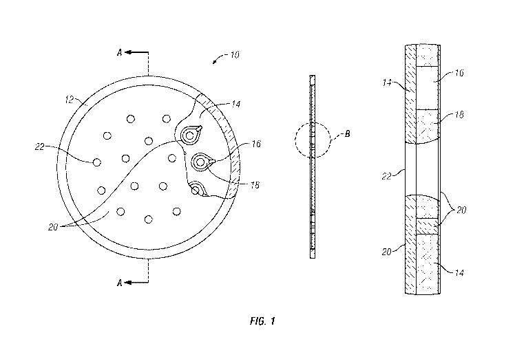
[0012] Fig. 1 is a schematic diagram of a discrete capacitor connector
insert with
planar conductive elastomer construction according to the invention;
[0013] Fig. 2 is a schematic diagram of a conductive elastomer
capacitor according
to the invention;
[0014] Fig. 3 is a schematic diagram of a conductive elastomer
capacitor integrated
into a connector insert according to the invention;
[0015] Fig. 4 is a schematic diagram of a conductive elastomer
"perimeter"
capacitor integrated into a connector insert according to the invention;
-4-
[0016] Fig. 5 is a schematic diagram of a discrete capacitor connector
insert with
planar conductive elastomer construction integrated into a connector assembly
according
to the invention; and
[0017] Fig. 6 is a schematic diagram of an insert according to the
invention placed
into a pre-existing connector (retrofit).
DETAILED DESCRIPTION OF THE INVENTION
[0018] The present invention employs planar conductive layers rather
than the wire
interconnects within a connector insert, which provides a number of
advantages. The
conductive layers can be conductive elastomer or other conductive element(s)
such as a
thin metal sheet, but the preferred construct is conductive silicone
elastomer, with a volume
resistivity preferably less than about 0.010 ohms-cm. Electrically opposing
conductive
layers are insulated from each other by the non-conductive elastomer. A
surface mount
device, such as a 0402 sized capacitor, transient voltage suppressor, or
resistor, is
connected between the two conductive layers. This planar arrangement of the
conductors
greatly reduces unwanted stray inductance. Further, a small capacitor can be
formed by
overlapping the opposing conductors and separating them with a thin layer of
non-conductive
elastomer, or other non-conductive material with high dielectric constant,
such as polypropylene. A
relative permittivity greater than 2 is preferred for any of these non-
conductive layers. The planar
construction of this integrated capacitor, and the elimination of a discrete
capacitor, yields
ultra-low stray inductance, providing effective filtering well into the GHz
frequencies. An
insert can employ a discrete device and/or an integral capacitor to achieve a
parallel
configuration, with the discrete device providing filtering at lower
frequencies and the
integral capacitor taking over at higher frequencies.
[0019] In addition to being installed at the mating interface of a
connector pair in a
retrofit manner, this assembly can be built into a single connector half,
creating a filtered
connector. Two capacitive inserts, separated by an inductive element, can be
built into a
connector, thereby creating a Pi filter. A "T" or "L" type filter can be
similarly configured.
CA 2960991 2019-10-28
, ,
CA 02960991 2017-03-10
-5-
[0020] This type of electronic circuit construction, utilizing
flexible conductive
elastomer interconnections between circuit elements and external electrical
contacts, has
application in fields other than electrical connectors, such as medical and
consumer
electronics where the circuitry is required to be compressed or flexed.
[0021] Turning to the figures, Fig. 1 shows one possible construction
of a discrete
capacitor connector insert 10 with planar conductive elastomer layers,
comprising
conductive elastomer shell contact 12, conductive elastomer ground plane 14,
capacitor 16, conductive elastomer pin contact 18, non-conductive elastomer
20, and pin
holes 22. This insert would typically be installed over the pins of a high
reliability circular
connector to provide EMI filtering.
[0022] Contact to each pin is made using a layer of conductive
elastomer with a
hole therein. The diameter of the hole is preferably smaller than the pin
diameter, so that
when the pin is inserted, the conductive elastomer stretches to accommodate
it. This
stretching of the conductive elastomer results in a tight fit around the pin,
and electrical
contact from the pin to the conductive elastomer is thereby achieved. One end
of a surface
mount device, e.g., a 0402 SMD capacitor, is placed so that it makes contact
to the
conductive elastomer pin contact. The other end of the capacitor makes contact
with the
planar conductive elastomer ground plane. The pin contact and the ground plane
are
separated from each other with a layer of non-conductive elastomer placed
between them.
The conductive ground plane is exposed around the periphery of the insert and
along the
top surface periphery. Its outside diameter is slightly larger than the
connector shell's
inside diameter, so that it is compressed when installed, achieving electrical
contact with
the connector shell. It can also make contact to the mating connector shell
along the top
surface periphery. The resulting planar construction of the insert results in
a very low stray
inductance, and much better filtering performance, as compared to existing
technology.
[0023] Fig. 2 shows an example of a capacitor 16 created using
conductive
elastomer and non-conductive elastomer, comprising dielectric non-conductive
elastomer 20, conductive elastomer first terminal 24, and conductive elastomer
second
terminal 26. A capacitor comprises a plurality of conductive plates separated
by an
insulating material. The value of the capacitor is determined by the
overlapping surface
CA 02960991 2017-03-10
-6-
area of the plates, the distance between the plates, and the dielectric
constant of the
insulating material.
[0024] By using elastomers for both the conductive and insulating
components of a
capacitor, the resulting part can change shape through compression,
distension, flexure
and other external forces while maintaining its electrical performance and
mechanical
integrity.
[0025] This type of capacitor can be incorporated into a connector
insert as shown
in Fig. 3, comprising non-conductive elastomer 20, pin holes 22, conductive
elastomer pin
contact plate 28, and conductive elastomer ground plane 30. In this example,
the
conductive elastomer pin contact plate is positioned above the conductive
elastomer
ground plate and separated by a thin layer of non-conductive elastomer. The
overlapping
area of the two conductive elastomers, thickness of the non-conductive
elastomer layer,
and the dielectric constant of the insulating material determine the value of
the resulting
capacitor. Since no discrete device is used, the resulting filter is extremely
low inductance
and provides effective filtering well into the 10's of GHZ.
[0026] Instead of using overlapping layers, this type of capacitor can
also be
created using the perimeter of the conductive elastomer pin contact as one
plate, the
surface of the conductive elastomer ground plane around the pin contact as the
other plate,
and the gap between these surfaces filled with a non-conductive elastomer as
the dielectric
as shown in Fig. 4. This embodiment comprises conductive elastomer shell
contact 12,
conductive elastomer ground plane 14, conductive elastomer pin contact 18, non-
conductive elastomer 20, and pin holes 22. The perimeter of the conductive
elastomer pin
contact can be any shape, but the preferred shape is a circle. The surface
area of the
perimeter of the conductive elastomer pin contact, the thickness of the gap
filled with the
non-conductive elastomer and the dielectric constant of the non-conductive
elastomer
determine the value of the resulting capacitor. Since no discrete device is
used, the
resulting filter is extremely low inductance and provides effective filtering
well into the 10's
of GHZ.
[0027] With minor dimensional modifications, the embodiments described
above
can also be made an integral part of a connector as shown in Fig. 5, instead
of an insert
CA 02960991 2017-03-10
-7-
between a connector pair. This embodiment comprises conductive elastomer
ground
plane 14, capacitor 16, conductive elastomer pin contact 18, non-conductive
elastomer 20,
o-ring 32, interfacial seal 34, connector shell 36, pins 38, and connector
insert 40. One
example involves placing the assembly between the connector insert and the
interfacial
seal. This permits the necessary contact with the pins and the connector shell
while
preserving the mating and sealing features of a standard connector pair. With
further
modifications to a standard connector, the filter assembly can be installed
elsewhere within
the connector as well.
[0028] Fig. 6 illustrates placement of an insert 10 according to the
invention into a
pre-existing connector, thereby providing a retrofit improvement to the
connector. Insert 10
is shown as installed over pins 38 and as oriented with respect to interfacial
seal 34, o-
ring 32, and connector shell 36.
[0029] Note that in the specification and claims, "about" or
"approximately" means
within twenty percent (20%) of the numerical amount cited.
[0030] Although the invention has been described in detail with
particular reference
to these preferred embodiments, other embodiments can achieve the same
results.
Variations and modifications of the present invention will be obvious to those
skilled in the
art and it is intended to cover in the appended claims all such modifications
and
equivalents.