Note: Descriptions are shown in the official language in which they were submitted.
CA 2961329 2017-03-17
15-MCB-1465
CURRENT TRANSFORMER APPARATUS THAT IS MOUNTABLE
TO A CIRCUIT BOARD
BACKGROUND
Field
The disclosed and claimed concept relates generally to electronic
equipment and, more particularly, to a current transformer apparatus that is
electrically
connectable with and mountable to a circuit board such as a printed circuit
board.
Related Art
Numerous types of electronic equipment are known in the relevant art.
One type of electronic component is a current transformer which includes a
length of
wire that is wound into a coil to form a winding. The wire typically is
relatively thin, and
the ends of the wire are typically soldered to pins that are mounted on a
circuit board.
While such current transformers have been generally effective for their
intended
purposes, they have not been without limitation.
The soldered connections between the end of the wire and the pins that are
mounted to the circuit board have been difficult to make due to the thinness
of the wire
and the difficulty in handling the wire, and for other reasons. Also, the
soldered
connections between the ends of the wire and the pins that are mounted to the
circuit
board have been subject to breakage during movement of the current transformer
and
circuit board from one location to another and during installation.
Improvements thus
would be desirable.
SUMMARY
Accordingly, an improved current transformer apparatus is configured to
enable it to be electrically connected with and physically mounted to a
circuit board. The
current transformer apparatus includes a support upon which a coil is situated
and upon
which a plurality of approximately U-shaped electrical connectors are also
situated. The
electrical connectors each include an electrical contact that is biased toward
a reaction
structure, and in the depicted exemplary embodiment the electrical contact and
the
reaction structure are both a part of the electrical connector. A circuit
board is received
between the electrical contact and the reaction structure, and the bias
between the
1
CA 2961329 2017-03-17
15-MCB-1465
electrical contact and the reaction structure mounts current transformer
apparatus to the
circuit board and provides an electrical connection therebetween.
An aspect of the disclosed and claimed concept is to provide an improved
current transformer apparatus that is easily mountable on and removable from a
circuit
board.
Another aspect of the disclosed and claimed concept is to provide such an
improved current transformer apparatus that avoids the need to provide
soldered
electrical connections between the ends of the wire of an electrical winding
and pins that
have been mounted to a circuit board.
Accordingly, an aspect of the disclosed and claimed concept is to provide
an improved current transformer apparatus that is structured to be
electrically connected
with and to be mounted to a circuit board. The current transformer apparatus
can be
generally stated as including a coil apparatus comprising a wire that is wound
into a coil,
a support, the coil apparatus being situated on the support, a connection
apparatus that
can be generally stated as including a plurality of electrical contacts and a
number of
reaction structures situated on the support, the plurality of electrical
contacts can be
generally stated as including a pair of electrical contacts, an electrical
contact of the pair
of electrical contacts having an electrical connection with the wire, another
electrical
contact of the pair of electrical contacts having another electrical
connection with the
wire, at least one of the at least first reaction structure and the plurality
of electrical
contacts being biased generally toward the other of the at least first
reaction structure and
the plurality of electrical contacts and being structured to engage the
circuit board
between the plurality of electrical contacts and the at least first reaction
structure to
mount the current transformer apparatus to the circuit board.
BRIEF DESCRIPTION OF THE DRAWINGS
A further understanding of the disclosed and claimed concept can be
gained from the following Description when read in conjunction with the
accompanying
drawings in which:
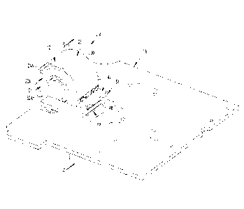
Fig. 1 is a perspective view of an improved current transformer apparatus
in accordance with a first embodiment of the disclosed and claimed concept
that is
mounted to a circuit board;
2
CA 2961329 2017-03-17
15-MCB-1465
Fig. 2 is a view similar to Fig. 1, except depicting the current transformer
apparatus being exploded away from the circuit board;
Fig. 3 is an enlarged perspective view of the current transformer apparatus
of Figs. 1 and 2;
Fig. 4 is an exploded view of the current transformer apparatus of Fig. 3;
Fig. 5 is a sectional view as taken along line 5-5 of Fig. 1;
Fig. 6 is a perspective view of an improved current transformer apparatus
in accordance with a second embodiment of the disclosed and claimed concept;
and
Fig. 7 is an exploded view of the current transformer apparatus of Fig. 6.
Similar numerals refer to similar parts throughout the specification.
DESCRIPTION
An improved current transformer apparatus 4 in accordance with a first
embodiment of the disclosed and claimed concept is depicted generally in Figs.
1-5. The
current transformer apparatus 4 includes a coil apparatus 6, and it further
includes a
support 10 upon which the coil apparatus 6 is situated. The current
transformer apparatus
4 additionally includes a connection apparatus 12 that is likewise situated on
the support
10.
The current transformer apparatus 4 is advantageously configured to
enable it to be mounted onto a circuit board 16, i.e., physically and directly
situated on
the circuit board 16 such as is depicted in Fig. 1, and to be simultaneously
electrically
connected with the circuit board 16. The circuit board 16 includes a number of
electrically conductive pads 18 that are depicted generally in Fig. 2 and
which are
electrically connected with various conductors and components that are
situated on the
circuit board 16 or elsewhere and which enable analysis of signals that are
detected from
the coil apparatus 6. As employed herein, the expression "a number of" and
variations
thereof shall refer broadly to any non-zero quantity, including a quantity of
one. As will
be set forth in greater detail below, the connection apparatus 12 is
electrically
connectable with the pads 18 to enable the current transformer apparatus 4 to
be
electrically connected with the circuit board 16.
The coil apparatus 6 includes a pair of coils 22A and 22B that each
include a length of wire 24A and 24B, respectively, each having a pair of
opposite ends
3
CA 2961329 2017-03-17
15-MCB-1465
38. The wires 24A and 24B are each wound in an approximately cylindrical shape
to
form the windings that can be said to make up the coils 22A and 22B.
The support 10 can be said to include a housing 28 that includes an
approximately annular wall 30 that surrounds a pair of sockets 32A and 32B
within
which the coils 22A and 22B, respectively, are received. The housing 28
further includes
a base 34 that is situated on the wall 30. The wall 30 has a pair of openings
36A and 36B
formed therein adjacent the base 34 through which the ends 38 of the wires 24A
and 24B
extend for connection with the connection apparatus 12. The exemplary openings
36A
and 36B are in the form of elongated slots but can be of other shapes without
departing
from the spirit of the present concept.
As can be understood from Figs. 3 and 4, the base 34 can be said to
include a platform 40 that is situated on the wall 30 and to further include a
covering wall
42 that is situated on the platform 40. The platform 40 has an elongated slot
46 formed
therein that receives an end of the circuit board 16 in a fashion that will be
described in
greater detail below.
The platform 40 includes a base wall 48 that is situated opposite the
covering wall 42. The platform further includes a pair of lateral abutments
52A and 52B
that are approximately L-shaped and which have a portion that extends along
the ends of
the base wall 48 and another portion that extends along the wall 30. The
platform 40
further includes a frontal abutment 54 that extends between the lateral
abutments 52A
and 52B along the edge of the base wall 48 that is opposite the wall 30.
Furthermore, the
platform 40 includes a plurality of dividers 58 that each include a first
portion 60 that
extends along the base wall 48, a second portion 62 that extends along the
wall 30, and a
third portion 64 that protrudes from the wall 30 and which extends
approximately parallel
the corresponding first portion 60. The platform 40 further includes a pair of
additional
lateral abutments 68A and 68B that protrude from the wall 30 and which extend
parallel
with the third portions 64. Further, the platform 40 includes an additional
frontal
abutment 70 that extends along the free ends of the third portions 64 and the
free ends of
the additional lateral abutments 68A and 68B opposite the wall 30. In the
depicted
exemplary embodiment, the wall 30 and the platform 40 are co-formed as a
single piece
unit, such as by molding and the like, from an electrically insulative
material such as a
4
CA 2961329 2017-03-17
15-MCB-1465
polymeric material or other appropriate material. As such, the various
components of the
platform 40 mentioned above are affixed to one another and are co-formed
together as a
single component.
As can thus be seen in Fig. 4, the covering wall 42 has a set of notches 74
formed in an edge thereof for receiving parts of the connection apparatus 12
therethrough
in a fashion that will be set forth in greater detail below. The covering wall
42 further
includes a set of latches 76 at opposite ends thereof that are receivable in a
set of seats 80
that are formed in the additional lateral abutments 68A and 68B of the
platform 40. The
latches 76, when received in the seats 80, affix the covering wall 42 to the
platform 40.
As is thus shown in Fig. 4, the connection apparatus 12 includes a
plurality of electrical connectors 82 that are each of an approximately U-
shaped
configuration and which can be said to include a solid leg 86 and a perforated
leg 80 that
has an elongated void region 92 formed therein. The perforated leg 88 and the
solid leg
86 are connected with one another at a junction 94. Each electrical connector
82 further
includes an elongated pin 90 that protrudes from the junction 94 and which is
formed out
of the material that was removed from the void region 92. The electrical
connectors 82
are each formed of an electrically conductive and flexible material such as
copper or
another metal and may have additional plating. The pins 90 are received in the
notches
74 and are soldered to the ends 38 of the wires 24A and 24B, with each
electrical
connector 82 being soldered with a single one of the four ends 38. As such,
the wire 24A
has a pair of the electrical connectors 28 connected at the opposite ends 38
thereof, and
the wire 24B likewise has another pair of the electrical connectors 82
connected with the
opposite ends 38 thereof.
Since the electrical connectors 82 are formed of a conductive material, it
can be understood that the solid leg 86, the perforated leg 88, and the
junction 94 are all
electrically conductive. However, the solid leg 86 and the perforated leg 88
in a free state
are separated from one another by a distance that is less than the thickness
of the circuit
board 16, and when the circuit board 16 is received in the slot 46 and between
the solid
leg 86 and the perforated leg 88, the solid leg 86 and the perforated leg 88
are elastically
deflected away from one another and are thus biased toward one another via
their
connection with one another at the junction 94.
5
CA 2961329 2017-03-17
15-MCB-1465
From a mechanical standpoint, it can be understood that the solid leg 86
and the perforated leg 88 each apply a compressive load toward the circuit
board 16 when
the circuit board 16 is received therebetween. As such, at least one of the
solid leg 86
and the perforated leg 88 can be said to form an electrical contact 96 that is
electrically
connected with the circuit board 16 by becoming electrically connected with
one of the
pads 18 when the circuit board 16 is received in the slot 46 and is
compressively engaged
between the solid leg 86 and the perforated leg 88. It is noted that in the
depicted
exemplary embodiment the electrical contact 96 is at least a portion of the
perforated leg
88. In a similar fashion, the electrical connectors 82 can each be said to
include a
reaction structure 98 that opposes the bias of the electrical contact 96 and
which, in the
depicted exemplary embodiment, is at least a portion of the solid leg 86. It
is noted that,
depending upon the configuration of the electrical connectors 82, the platform
40 or the
base wall 48 can be said to additionally or alternatively form a part of the
reaction
structure 98 that opposes the bias of the electrical contact 96. This
principle can be
understood if the system employed alternative electrical connectors that did
not
additionally include the solid leg 86 and rather included electrical contacts
that were
spring biased or otherwise biased in a direction toward the base wall 48. In
such a
situation, the base wall 48 and other structures of the platform 40 would
serve as the
reaction structure that is situated to oppose the bias by the aforementioned
alternative
electrical contacts. In the depicted exemplary embodiment, however, the
electrical
connectors 82 are generally U-shaped and each include both the electrical
contact 96 and
the reaction structure 98.
As can be understood from Figs. 3 and 4, the various aforementioned
structures of the platform 40 form thereon a set of receptacles 99, each of
which receives
therein a corresponding one of the electrical connectors 82. The dividers 58
are situated
between adjacent pairs of the electrical connectors 82 and serve to
electrically isolate
each electrical connector 82 from one another. Additionally, the lateral
abutments 52A
and 52B, the frontal abutment 54, the additional lateral abutments 68A and
68B, and the
additional frontal abutment 70 serve to retain the electrical connectors 82 in
a position
situated between the covering wall 42 and the base wall 48, meaning that they
6
CA 2961329 2017-03-17
15-MCB-1465
mechanically engage the electrical connectors 82 and resist movement of the
electrical
connectors 82 in directions away from the wall 30 and away from the base 34.
By securing the electrical connectors 82 on the base 34, the electrical
connectors 82 are generally immovable with respect to the support 10 apart
from elastic
deformation of the solid leg 86 or the perforated leg 88 or both when the
circuit board 16
is received between the solid leg 86 and the perforated leg 88 and is removed
therefrom.
Such advantageous retention of the electrical connectors 82 on the base 34
correspondingly resists movement of the pins 90 with respect to the wires 24A
and 24B,
which helps to maintain the integrity of the soldered connection between the
pins 90 and
the ends 38. Movement of the pins 90 is further resisted by the reception of
the pins 90 in
the notches 74 and the reception of the latches 76 in the seats 80, which
serves to clamp
the pins 90 against the wall 30.
As such, the current transformer apparatus 4 can be repeatedly received on
the circuit board 16, thereby mounting the current transformer apparatus 4 to
the circuit
board 16 and providing an electrical connection therebetween, and removed from
the
circuit board 16 without a meaningful risk of damaging the electrical
connection between
the ends 38 and the pins 90. The current transformer apparatus 4 thus
advantageously
can be easily mounted to the circuit board 16 and electrically connected
therewith simply
by slidingly receiving the circuit board 16 in the slot 46 to thereby
electrically connect
together the pads 18 with the electrical connectors 82 and thus with the ends
of the wires
24A and 24B that form the coils 22A and 22B. The improved current transformer
apparatus 4 is thus simple to manufacture and simple to install and remove as
needed and
is mechanically and electrically reliable. Other advantages will be apparent.
An improved current transformer apparatus 104 in accordance with a
second embodiment of the disclosed and claimed concept is depicted generally
in Figs. 6
and 7. The current transformer apparatus 104 is similar to the current
transformer
apparatus 4 except that it includes a coil apparatus 106 that includes only a
single coil
122. A support 110 of the current transformer apparatus 104 is thus configured
with only
a single socket 132 to receive the coil 122 therein. Likewise, a connection
apparatus 112
of the current transformer apparatus 104 includes only a pair of electrical
connectors 182
that are similar to the electrical connectors 82 and are electrically
connected with the ends
7
CA 2961329 2017-03-17
15-MCB-1465
of a wire that forms the coil 122. It can be seen from Figs. 6 and 7 that the
support 110
has formed therein a pair of openings 136 that are in the form of discrete
holes rather than
elongated slots, but it is understood that the openings 136 could be of other
configurations without departing from the spirit of the present concept.
The current transformer apparatus 104 is receivable on a circuit board in
the same way in which the current transformer apparatus 4 is receivable on the
circuit
board 16. If desired, a pair of the current transformer apparatuses 104 can be
mounted to
the circuit board 16 and electrically connected with the pads 18 inasmuch as a
pair of the
current transformer apparatuses 104 can be substituted for and are
substantially
equivalent to the current transformer apparatus 4. The current transformer
apparatus 104
can also be used individually.
It thus can be seen that the current transformer apparatus 104 is similar to
the current transformer apparatus 4 except that is includes only a single coil
122 and is
suitable for applications that require only a single coil. The current
transformer apparatus
104 is also suitable for other applications in which a plurality of the
current transformer
apparatuses 104 can be used in conjunction with one another. Other advantages
will be
apparent.
While specific embodiments of the disclosed concept have been described
in detail, it will be appreciated by those skilled in the art that various
modifications and
alternatives to those details could be developed in light of the overall
teachings of the
disclosure. Accordingly, the particular arrangements disclosed are meant to be
illustrative only and not limiting as to the scope of the disclosed concept
which is to be
given the full breadth of the claims appended and any and all equivalents
thereof.
8