Note: Descriptions are shown in the official language in which they were submitted.
83990624
DISTRIBUTED POWER RECEIVING ELEMENTS FOR
WIRELESS POWER TRANSFER
CROSS REFERENCE TO RELATED APPLICATIONS
[0001] This application is entitled to and claims the benefit of the filing
date of U.S.
Provisional App. No. 62/065,918 filed October 20, 2014.
[0002] This application also claims priority to U.S. Application No.
14/630,996 filed
February 25, 2015.
TECHNICAL FIELD
[0003] The present disclosure relates generally to wireless power transfer
systems. More
particularly, the present disclosure relates to electronic devices having
configurations of
distributed power receiving elements for wireless power transfer.
BACKGROUND
[0004] Unless otherwise indicated, the foregoing is not admitted to be prior
art to the claims
recited herein and should not be construed as such.
[0005] Providing an adequate resonator in a power receiving unit (PRU) of a
wireless
charging system in an electronic device can be challenging. For example, in a
mobile device,
restrictions on how the back cover of the mobile device may be used can create
challenges for
the design and placement of a resonator for wireless charging. Manufacturers
of mobile
devices may specify "keep out" areas on their device designs in order not to
impact
performance of the antenna system that provide communication for the mobile
device.
Consequently, only small areas may be available for a wireless charging
resonator so the
resonator may be too small to generate adequate power for the mobile device.
[0006] The form factor of the electronic device itself may pose challenges in
terms of its
three dimensional structure. For example, the shape of the electronic device
may not
1
Date recue / Date received 2021-11-05
CA 02962109 2017-03-21
WO 2016/064551
PCT/US2015/053501
allow for practical placement of a resonator. The electronic device may be too
small to
support a resonator. In some instances, the electronic device may be made of a
conductive medium where wireless power transfer is difficult.
SUMMARY
[0007] The present disclosure describes apparatus for wireless charging
including a
casing that comprises one or more electrically separate, electrically
conductive
segments. The apparatus may include power receiving elements configured to
couple to
an externally generated magnetic field to wirelessly power or charge a load.
In
accordance with aspects of the present disclosure, at least one of the power
receiving
elements may be an electrically conductive segment of the casing. In
accordance with
aspects of the present disclosure, a first power receiving element and a
second power
receiving element may be connected together.
[0008] In accordance with aspects of the present disclosure, one of the power
receiving elements may be a coil of wire.
[0009] In accordance with aspects of the present disclosure, the apparatus may
include
switches to selectively connect together the power receiving elements in
different
combinations. In some aspects, the different combinations may exhibit
different
degrees of mutual coupling with the externally generated magnetic field. In
some
aspects, the different combinations may exhibit different output voltages. In
some
aspects, the different combinations may exhibit different resistances.
[0010] In accordance with aspects of the present disclosure, the externally
generated
magnetic field may be generated from a source that is vertically spaced apart
from the
apparatus. In accordance with aspects of the present disclosure, the
externally generated
magnetic field may generated from a source that is horizontally spaced apart
from the
apparatus.
[0011] The present disclosure describes apparatus for wirelessly receiving
power,
including a casing that constitutes a portion of a housing of an electronic
device. The
apparatus may include a first power receiving element configured to wirelessly
receive
power via an externally generated alternating magnetic field. In accordance
with
aspects of the present disclosure, the first power receiving element may be a
coil of
conductive material attached to the casing. The apparatus may include a second
power
2
CA 02962109 2017-03-21
WO 2016/064551
PCT/US2015/053501
receiving element configured to wirelessly receive power via the externally
generated
alternating magnetic field. In accordance with aspects of the present
disclosure, the
second power receiving element may be an electrically conductive segment
comprising
the casing.
[0012] In accordance with aspects of the present disclosure, the coil of
conductive
material that constitutes the first power receiving element may be
electrically connected
to the electrically conductive segment of the casing that constitutes the
second power
receiving element.
[0013] In accordance with aspects of the present disclosure, the apparatus may
include
a plurality of power receiving elements, including the first and second power
receiving
elements. The apparatus may include a plurality of switches operable to
connect
together different combinations of power receiving elements.
[0014] The present disclosure describes apparatus for wirelessly receiving
power,
comprising means for housing an electronic device, first means for receiving
power
through an externally generated magnetic field, and second means for receiving
power
through an externally generated magnetic field comprising a portion of the
means for
housing the electronic device.
[0015] The present disclosure describes a method for wirelessly receiving
power,
including producing a first current through electromagnetic induction at a
first location
in a device, producing a second current through electromagnetic induction at a
second
location in the device, and combining the first current and the second current
to produce
power for the device.
[0016] In accordance with aspects of the present disclosure, producing the
first current
may include coupling a first coil of wire to the externally generated magnetic
field. In
accordance with aspects of the present disclosure, producing the second
current may
include coupling a portion of a metallic casing that houses the device to the
externally
generated magnetic field.
[0017] The present disclosure describes an apparatus for wirelessly receiving
power,
including a casing for a power receiving unit (PRU) and power receiving
elements
distributed at different locations on the casing. The apparatus may include a
combining
circuit and switches to connect a subset of the power receiving elements to
the
3
CA 02962109 2017-03-21
WO 2016/064551
PCT/US2015/053501
combining circuit. The combining circuit may be configured to combine the
subset of
power receiving elements to form a set of connected power receiving elements.
The
apparatus may include a controller configured to operate the plurality of
switches and
the combining circuit.
[0018] In accordance with aspects of the present disclosure, the apparatus may
include
a rectifier circuit connected to an output of the combining circuit to produce
an output
voltage. In accordance with aspects of the present disclosure, the combining
circuit may
be configured to selectively connect together a subset of power receiving
elements in
series fashion and/or in parallel fashion.
[0019] In accordance with aspects of the present disclosure, apparatus may
include
rectifier circuits connected to respective power receiving elements to output
respective
DC levels. The outputs of the rectifier circuits may be connected to the
combining
circuit. In accordance with aspects of the present disclosure, the combining
circuit may
be configured to selectively add and/or subtract DC levels associated with the
subset of
power receiving elements.
[0020] The present disclosure describes an apparatus wirelessly receiving
power,
comprising means for housing a power receiving unit (PRU), a plurality of
means for
receiving power through an externally generated magnetic field, the plurality
of means
for receiving power distributed at different locations on the means for
housing the PRU,
and means for selectively combining a one or more of the plurality of means
for
receiving power to form a set of connected power receiving elements.
[0021] The present disclosure describes a method for wirelessly receiving
power,
including coupling power receiving elements to an externally generated
magnetic field
at different locations in a device, connecting together a subset of the
receiving elements,
and combining current induced in the subset of the receiving elements to
produce power
for the device. In accordance with aspects of the present disclosure, coupling
power
receiving elements to the externally generated magnetic field includes one or
more of
coupling a coil of wire to the externally generated magnetic field and
coupling a portion
of a metallic casing that houses the device to the externally generated
magnetic field.
[0022] In accordance with aspects of the present disclosure, the method may
include
rectifying a combined current subsequent to combining the current induced in
the subset
of the power receiving elements. In accordance with aspects of the present
disclosure,
4
83990624
the method may include rectifying current induced in subset of the power
receiving elements
prior to the combining.
[0022a] According to one aspect of the present invention, there is
provided an
apparatus for wireless charging, comprising: a casing comprising one or more
electrically
separate, electrically conductive segments; and a plurality of power receiving
elements
configured to couple to an externally generated magnetic field to wirelessly
power or charge a
load, at least one of the plurality of power receiving elements comprising one
of the
electrically conductive segments of the casing, at least a first power
receiving element and a
second power receiving element connected together and operative to produce a
single output
of power when coupled to the externally generated magnetic field.
[0022b] According to another aspect of the present invention, there is
provided an
apparatus for wirelessly receiving power, the apparatus comprising: a casing
that constitutes a
portion of a housing of an electronic device, the casing having at least one
electrically
conductive segment; a first power receiving element configured to wirelessly
receive power
via an externally generated alternating magnetic field, the first power
receiving element
comprising a coil of conductive material attached to the casing; and at least
a second power
receiving element configured to wirelessly receive power via the externally
generated
alternating magnetic field, the second power receiving element comprising the
at least one
electrically conductive segment of the casing.
[0022c] According to another aspect of the present invention, there is
provided an
apparatus for wirelessly receiving power, the apparatus comprising: means for
housing an
electronic device including at least one metal segment; first means for
receiving power
through an externally generated magnetic field; second means for receiving
power through the
externally generated magnetic field comprising a portion of the at least one
metal segment.
[0022d] According to another aspect of the present invention, there is
provided a
method for wirelessly receiving power comprising: producing a first current
through
electromagnetic induction at a first location in a device; producing a second
current through
electromagnetic induction at a second location in the device; and combining
the first current
Date recue / Date received 2021-11-05
83990624
and the second current to produce power for the device; wherein producing a
first current
includes coupling a first coil of wire to an externally generated magnetic
field and producing a
second current includes coupling a portion of metallic casing that houses the
device to the
externally generated magnetic field.
[0022e] According to another aspect of the present invention, there is
provided an
apparatus for wirelessly receiving power, the apparatus comprising: a casing
for a portable
electronic device; a plurality of power receiving elements distributed at
different locations on
the casing; a combining circuit; a plurality of switches configured to connect
a subset of the
plurality of power receiving elements to the combining circuit, the combining
circuit
configured to combine the subset of the plurality of power receiving elements
to form a set of
connected power receiving elements; and a controller configured to operate the
plurality of
switches and the combining circuit.
1002211 According to another aspect of the present invention, there is
provided a
method for wirelessly receiving power, comprising: coupling power receiving
elements to an
externally generated magnetic field at different locations in a device;
connecting together a
subset of the receiving elements; and combining current induced in the subset
of the receiving
elements to produce power for the device; wherein coupling power receiving
elements to the
externally generated magnetic field includes one or more of coupling a coil of
wire to the
externally generated magnetic field and coupling a portion of a metallic
casing that houses the
device to the externally generated magnetic field.
[0023] The following detailed description and accompanying drawings provide a
better
understanding of the nature and advantages of the present disclosure.
BRIEF DESCRIPTION OF THE DRAWINGS
100241 With respect to the discussion to follow and in particular to the
drawings, it is
stressed that the particulars shown represent examples for purposes of
illustrative discussion,
and are presented in the cause of providing a description of principles and
conceptual aspects
of the present disclosure. In this regard, no attempt is made to show
implementation details
beyond what is needed for a fundamental understanding of the present
disclosure. The
5a
Date recue / Date received 2021-11-05
83990624
discussion to follow, in conjunction with the drawings, makes apparent to
those of skill in the
art how embodiments in accordance with the present disclosure may be
practiced. In the
accompanying drawings:
[0025] Fig. 1 is a functional block diagram of a wireless power transfer
system in
accordance with an illustrative embodiment.
[0026] Fig. 2 is a functional block diagram of a wireless power transfer
system in
accordance with an illustrative embodiment.
[0027] Fig. 3 is a schematic diagram of a portion of transmit circuitry or
receive circuitry of
Fig. 2 including a power transmitting or receiving element in accordance with
an illustrative
embodiment.
[0028] Fig. 4 illustrates an embodiment of a system of distributed receiving
elements in
accordance with the present disclosure.
[0029] Fig. 4A shows a schematic representation of a casing in accordance with
the present
disclosure.
[0030] Fig. 5 illustrates an embodiment of distributed receiving elements in
accordance with
the present disclosure.
[0031] Figs 6 and 6A illustrate receiving elements using segments of a casing
for a PRU.
5b
Date recue / Date received 2021-11-05
CA 02962109 2017-03-21
WO 2016/064551
PCT/US2015/053501
[0032] Figs. 7 and 7A-1 illustrate a configuration of receiving elements in
accordance
with the present disclosure.
[0033] Fig. 8 illustrates a configuration of receiving elements in accordance
with the
present disclosure.
[0034] Figs. 9, 9A-1, 9A-2 illustrate configurations of receiving elements in
accordance with the present disclosure.
[0035] Figs. 10 and 10A-1 illustrate a configuration of receiving elements in
accordance with the present disclosure.
[0036] Figs. 10A, 10B, 10C, and 10D depict models of a casing configured with
receiving elements in accordance with the present disclosure.
[0037] Figs. 11A and 11B illustrate a vertical configuration of a PTU and PRU
in
accordance with the present disclosure.
[0038] Figs. 11C and IID illustrate side-by-side configurations of a PTU and
PRU in
accordance with the present disclosure.
[0039] Figs. 12A, 12B, and 12C illustrate aspects of a system of receiving
elements in
a wearable device in accordance with the present disclosure.
[0040] Fig. 13 illustrates selectively connectable combinations of receiving
elements
based on mutual inductance in accordance with the present disclosure.
[0041] Fig. 14 illustrates selectively connectable combinations of receiving
elements
based on voltage in accordance with the present disclosure.
[0042] Fig. 15 illustrates selectively connectable combinations of receiving
elements
based on resistance in accordance with the present disclosure.
[0043] Fig. 16 illustrates selectively connectable combinations of receiving
elements
in accordance with the present disclosure.
[0044] Fig. 17 illustrates selectively connectable combinations of receiving
elements
using feedback in accordance with the present disclosure.
6
CA 02962109 2017-03-21
WO 2016/064551
PCT/US2015/053501
DETAILED DESCRIPTION
[0045] In the following description, for purposes of explanation, numerous
examples
and specific details are set forth in order to provide a thorough
understanding of the
present disclosure. It will be evident, however, to one skilled in the art
that the present
disclosure as expressed in the claims may include some or all of the features
in these
examples, alone or in combination with other features described below, and may
further
include modifications and equivalents of the features and concepts described
herein.
[0046] Wireless power transfer may refer to transferring any form of energy
associated with electric fields, magnetic fields, electromagnetic fields, or
otherwise from
a transmitter to a receiver without the use of physical electrical conductors
(e.g., power
may be transferred through free space). The power output into a wireless field
(e.g., a
magnetic field or an electromagnetic field) may he received, captured by, or
coupled by
a "power receiving element" to achieve power transfer.
[0047] Fig. 1 is a functional block diagram of a wireless power transfer
system 100, in
accordance with an illustrative embodiment. Input power 102 may be provided to
a
transmitter 104 from a power source (not shown in this figure) to generate a
wireless
(e.g., magnetic or electromagnetic) field 105 for performing energy transfer.
A receiver
108 may couple to the wireless field 105 and generate output power 110 for
storing or
consumption by a device (not shown in this figure) coupled to the output power
110.
The transmitter 104 and the receiver 108 may be separated by a distance 112.
The
transmitter 104 may include a power transmitting element 114 for
transmitting/coupling
energy to the receiver 108. The receiver 108 may include a power receiving
element
118 for receiving or capturing/coupling energy transmitted from the
transmitter 104.
[0048] In one illustrative embodiment, the transmitter 104 and the receiver
108 may
be configured according to a mutual resonant relationship. When the resonant
frequency of the receiver 108 and the resonant frequency of the transmitter
104 are
substantially the same or very close, transmission losses between the
transmitter 104
and the receiver 108 are reduced. As such, wireless power transfer may be
provided
over a larger distances. Resonant inductive coupling techniques may thus allow
for
improved efficiency and power transfer over various distances and with a
variety of
inductive power transmitting and receiving clement configurations.
7
CA 02962109 2017-03-21
WO 2016/064551
PCT/1JS2015/053501
[0049] In certain embodiments, the wireless field 105 may correspond to the
"near
field" of the transmitter 104 as will be further described below. The near-
field may
correspond to a region in which there are strong reactive fields resulting
from the
currents and charges in the power transmitting element 114 that minimally
radiate
power away from the power transmitting element 114. The near-field may
correspond
to a region that is within about one wavelength (or a fraction thereof) of the
power
transmitting element 114.
[0050] In certain embodiments, efficient energy transfer may occur by coupling
a
large portion of the energy in the wireless field 105 to the power receiving
element 118
rather than propagating most of the energy in an electromagnetic wave to the
far field.
[0051] In certain implementations, the transmitter 104 may output a time
varying
magnetic (or electromagnetic) field with a frequency corresponding to the
resonant
frequency of the power transmitting element 114. When the receiver 108 is
within the
wireless field 105, the time varying magnetic (or electromagnetic) field may
induce a
current in the power receiving element 118. As described above, if the power
receiving
element 118 is configured as a resonant circuit to resonate at the frequency
of the power
transmitting element 114, energy may be efficiently transferred. An
alternating current
(AC) signal induced in the power receiving element 118 may be rectified to
produce a
direct current (DC) signal that may be provided to charge or to power a load.
[0052] Fig. 2 is a functional block diagram of a wireless power transfer
system 200, in
accordance with another illustrative embodiment. The system 200 may include a
transmitter 204 and a receiver 208. The transmitter 204 (also referred to
herein as
power transfer unit, PTU) may include transmit circuitry 206 that may include
an
oscillator 222, a driver circuit 224, and a filter and matching circuit 226.
The oscillator
222 may be configured to generate a signal at a desired frequency that may
adjust in
response to a frequency control signal 223. The oscillator 222 may provide the
oscillator signal to the driver circuit 224. The driver circuit 224 may be
configured to
drive the power transmitting element 214 at, for example, a resonant frequency
of the
power transmitting element 214 based on an input voltage signal (VD) 225. The
driver
circuit 224 may be a switching amplifier configured to receive a square wave
from the
oscillator 222 and output a sine wave.
8
CA 02962109 2017-03-21
WO 2016/064551
PCT/1JS2015/053501
[0053] The filter and matching circuit 226 may filter out harmonics or other
unwanted
frequencies and match the impedance of the transmitter 204 to the power
transmitting
element 214. As a result of driving the power transmitting element 214, the
power
transmitting element 214 may generate a wireless field 205 to wirelessly
output power at
a level sufficient for charging a battery 236, or otherwise powering a load.
[0054] The receiver 208 (also referred to herein as power receiving unit, PRU)
may
include receive circuitry 210 that may include a matching circuit 232 and a
rectifier
circuit 234. The matching circuit 232 may match the impedance of the receive
circuitry
210 to the power receiving element 218. The rectifier circuit 234 may generate
a DC
power output from an AC power input to charge the battery 236, as shown in
Fig. 2.
The receiver 208 and the transmitter 204 may additionally communicate on a
separate
communication channel 219 (e.g., Bluetooth, Zigbee, cellular, etc.). The
receiver 208
and the transmitter 204 may alternatively communicate via in-band signaling
using
characteristics of the wireless field 205.
[0055] The receiver 208 may be configured to determine whether an amount of
power
transmitted by the transmitter 204 and received by the receiver 208 is
appropriate for
charging the battery 236. Transmitter 204 may be configured to generate a
predominantly non-radiative field with a direct field coupling coefficient (k)
for
providing energy transfer. Receiver 208 may directly couple to the wireless
field 205
and may generate an output power for storing or consumption by a battery (or
load) 236
coupled to the output or receive circuitry 210.
[0056] As discussed above, transmitter 204 and receiver 208 may be separated
by a
distance and may be configured according to a mutual resonant relationship to
minimize
transmission losses between the transmitter and the receiver.
[0057] Fig. 3 is a schematic diagram of a portion of the transmit circuitry
206 or the
receive circuitry 210 of Fig. 2, in accordance with illustrative embodiments.
As
illustrated in Fig. 3, transmit or receive circuitry 350 may include a power
transmitting
or receiving element 352. The power transmitting or receiving element 352 may
also be
referred to or be configured as an antenna or a "loop" antenna 352. The term
"antenna"
generally refers to a component that may wirelessly output or receive energy
for
coupling to another "antenna." The power transmitting or receiving element 352
may
also be referred to herein or be configured as a "magnetic" antenna, or an
induction coil,
9
CA 02962109 2017-03-21
WO 2016/064551
PCT/1JS2015/053501
a resonator, or a portion of a resonator. The power transmitting or receiving
element
352 may also be referred to as a coil or resonator of a type that is
configured to
wirelessly output or receive power. As used herein, the power transmitting or
receiving
element 352 is an example of a "power transfer component" of a type that is
configured
to wirelessly output and/or receive power. The power transmitting or receiving
element
352 may include an air core or a physical core such as a ferrite core (not
shown in this
figure).
[0058] When the power transmitting or receiving element 352 is configured as a
resonant circuit or resonator, the resonant frequency of the power
transmitting or
receiving element 352 may be based on the inductance and capacitance.
Inductance
may be simply the inductance created by a coil or other inductor forming the
power
transmitting or receiving element 352, whereas, capacitance (e.g., a
capacitor) may be
added to create a resonant structure at a desired resonant frequency. As a non
limiting
example, a capacitor 354 and a capacitor 356 may be added to the transmit or
receive
circuitry 350 to create a resonant circuit.
[0059] Other resonant circuits formed using other components are also
possible. As
another non limiting example, a capacitor (not shown) may be placed in
parallel
between the two terminals of the circuitry 350. For power transmitting
elements, the
signal 358, with a frequency that substantially corresponds to the resonant
frequency of
the power transmitting or receiving element 352, may be an input to the power
transmitting or receiving element 352. For power receiving elements, the
signal 358,
with a frequency that substantially corresponds to the resonant frequency of
the power
transmitting or receiving element 352, may be an output from the power
transmitting or
receiving element 352.
[0060] Generally, in accordance with the present disclosure, the power
receiving unit
(PRU) of a wireless charging system may comprise several power receiving
elements
distributed at different locations in the PRU that can receive power through
electromagnetic induction, for example, by coupling with an externally
generated
magnetic field. In some embodiments, the power receiving elements (referred to
herein
as "receiving elements") can individually produce power that can be combined
to
produce a single output of power. In other embodiments, some receiving
elements may
be connected together to produce power. A system of distributed receiving
elements
CA 02962109 2017-03-21
WO 2016/064551
PCT/US2015/053501
may be suitable for mobile devices where the space within such a device may
not allow
for a single receiving element of suitable size to provide adequate power
transfer
capacity.
[0061] In accordance with the present disclosure, receiving elements may
comprise
coils of wire (resonator coils) and/or segments of the housing of the
electronic device.
These aspects of the present disclosure will be discussed in more detail
below. In some
embodiments, the receiving elements may be connected in a resonant circuit to
form a
resonant power receiving element or "resonator"; see, for example, the circuit
in Fig. 3.
In other embodiments, the receiving elements may not be connected in a
resonant
circuit. In the figures and description that follow, it will be understood
that the
disclosed receiving elements may be connected in resonant circuits in some
embodiments, and may not he connected in resonant circuits in other
embodiments.
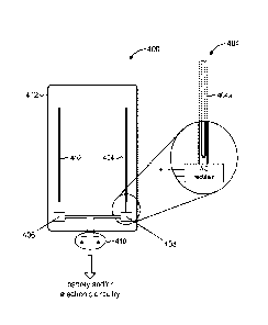
[0062] Referring to Fig. 4, a PRU 400 in accordance with some embodiments of
the
present disclosure may be configured with receiving elements 402, 404. Each
receiving
element 402, 404 may represent an example of means for receiving power through
an
externally generated magnetic field. In some embodiments, the receiving
elements 402,
404 may comprise a coil of wire or other suitable electrically conductive
medium. Fig.
4, for example, shows that receiving element 404 may comprise a coil of wire
404a
having two turns. In some embodiments, the receiving elements 402, 404 may be
connected in a resonant circuit. In other embodiments, the receiving elements
402. 404
may not be connected in a resonant circuit. Each receiving element 402, 404
may be
connected to respective AC rectifier circuits 406, 408, which can convert a
time-varying
signal (AC signal) to a DC voltage. In some embodiments, the AC rectifier
circuits 406,
408 may be full-wave rectifier circuits, or other suitable rectification
circuits known to
those of ordinary skill in the art. Output from the AC rectifiers 406, 408 may
be
connected in series to produce a single voltage at an output 410.
[0063] In some embodiments, the receiving elements 402, 404 may be attached to
interior surfaces of the casing that houses the PRU 400. Fig. 4A, for example,
is a
schematic representation of a casing 40 that may be configured as means for
housing a
PRU (e.g., for a mobile computing device or any portable computing device) in
accordance with the present disclosure. The figure shows examples of areas
44a, 44b,
44c in the PRU casing 40 that may incorporate communication antennas (not
shown);
11
CA 02962109 2017-03-21
WO 2016/064551
PCT/1JS2015/053501
e.g., cellular network, WiFiTM communication, Bluetooth communication, GPS,
etc.
The areas 44a, 44b, 44c may be referred to as "keep out" areas, because they
should be
free of obstructions that can impede proper signal transmission and/or
reception through
slots 42. Fig. 4A, for example, shows a receiving element 41a disposed above
the keep
out areas 44a, 44b and a receiving element 41b disposed below the keep out
areas 44a,
44b. In some embodiments, the receiving elements 41a, 41b may be separate
coils that
are connected together, for example, by connecting wires 45 that run between
the keep
out areas 44a, 44b. In other embodiments all or a portion of metal segments of
the
casing may form a receiving elements (e.g., the receiving element 41a) as will
be further
described below.
[0064] Ferrite tape 43a, 43b (or any ferromagnetic material) may be provided
between
the receiving elements 41a, 41b and the metal shell that comprises the casing
40 to
shield the metal shell from magnetic fields that can arise in the receiving
elements 41a,
41b due to induced currents in receiving elements 41a, 41b during wireless
power
transfer. In some embodiments, ferrite tape 43b may also be provided on top of
receiving element 41b to sandwich receiving element 41b. The upper ferrite
tape 43b
can shield nearby device electronics (not shown) that receiving element 41b
may come
into proximity with when the PRI J is assembled.
[0065] Returning to Fig. 4, in operation, when a power transfer unit (PTU, not
shown)
generates an external time-varying magnetic field, the externally generated
magnetic
field can couple to receiving elements 402, 404 to induce an AC current in the
receiving
elements 402, 404. In particular, a first current can be produced through
electromagnetic induction of receiving element 402 at a first location in PRU
400. A
second current can be produced through electromagnetic induction of receiving
element
404 at a second location in PRU 400. The AC rectifier circuits 406, 408 can
rectify the
AC currents that result in respective receiving elements 402, 404 to produce
respective
DC output voltages. The DC output voltages can then be combined to produce a
voltage at output 410 to provide power to the PRU 400.
[0066] In some embodiments, the receiving elements may be on separate
circuits. In
Fig. 4, for example, each receiving element 402, 404 is shown connected to its
respective AC rectifier circuit 406, 408. In other embodiments, the receiving
elements
may be connected together in series in a common circuit. Referring to Fig. 5,
for
12
CA 02962109 2017-03-21
WO 2016/064551
PCT/US2015/053501
example, a PRU 503 may comprise receiving elements 502, 504, 506. In some
embodiments, each receiving element 502, 504, 506 may be a coil of wire having
some
number of turns, see for example the coil of wire 404a in Fig. 4. The separate
coils of
wire comprising the receiving elements 502, 504, 506 may be connected together
in
series by connectors 512. The connectors 512 may be wires, conductive traces
on a
printed circuit board (PCB), and so on. As indicated in Fig. 5, for example,
one end of a
coil comprising receiving element 502 may be connected to an AC rectifier 508.
The
other end of receiving element 502 may be connected to one end of a coil
comprising
receiving element 504. The other end of the coil for receiving element 504 may
be
connected to one end of a coil comprising receiving element 506. Finally, the
other end
of the coil comprising receiving element 506 may be connected to the AC
rectifier 508.
[0067] In accordance with the present disclosure, at least some portions of
the casing
of the PRU itself can serve as receiving elements, if those portions of the
casing are
electrically conductive. Fig. 6, for example, illustrates a casing 600 that
may be
configured as means for housing a device (not shown) such as a smartphone, a
computer
tablet, etc. The casing 600, for example, may be the back cover of the device.
In some
embodiments, the casing 600 may comprise several electrically separate,
electrically
conductive segments 602, 604, 606. For example, segment 602 may be the upper
portion of the casing 600, segment 604 may be the middle portion of the casing
600, and
segment 606 may be the bottom portion of the casing 600. An electrically non-
conductive separator 608 may provide electrical separation between the
segments 602
and 604 to define a slot between segments 602 and 604. The non-conductive
separator
608 may include a T-segment 608' that defines a slot in the segment 604. An
electrically non-conductive separator 610 may provide electrical separation
between the
segments 604 and 606 to define a slot between segments 604 and 606.
[0068] In accordance with the present disclosure, the segments 602 ¨ 606 may
constitute inductive elements that can serve as receiving elements that
receive power
through electromagnetic induction, for example, by coupling to an externally
generated
magnetic field and thus give rise to eddy currents in the segments 602 ¨ 606
which can
be used to power a device (not shown). Each segment 602 ¨ 606 may have a
respective
feed location for providing an output for the eddy currents. For example, feed
location
612 may provide an output for eddy currents that can be induced in segment 604
during
13
CA 02962109 2017-03-21
WO 2016/064551
PCT/1JS2015/053501
wireless power transfer. Segments 602 ¨ 606 of casing 600 represent further
examples
of means for receiving power through an externally generated magnetic field
[0069] In some embodiments, some of the segments may be connected together by
connectors (jumper wires). For example, connector 622 may electrically connect
together segment 602 and segment 604. A feed location 614 may provide an
output for
eddy currents that may arise in segments 602 and 604 in response to being
coupled to an
externally generated magnetic field. Similarly, a connector 624 may
electrically
connect together segment 604 and segment 606. A feed location 616a may provide
an
output for eddy currents that may arise in segments 604 and 606. In some
embodiments, an additional feed location 616b may provide an additional output
for
eddy currents in segments 604 and 606.
[0070] Referring to Fig. 6A, the feeds 612, 614, 616a, 616b may connect to
respective
AC rectifier circuitry 632, 634, 636, 638 to produce respective DC voltage
levels. In
sonic embodiments, the AC rectifier circuitry 632 ¨ 638 may be part of the
device
electronics. Outputs of the AC rectifier circuitry 632 ¨ 638 may be connected
together
in series to produce a single DC output, such as illustrated for example by
the inset
illustrated in Fig. 6A.
[0071] In accordance with the present disclosure, a system of receiving
elements in a
PRU may comprise coils (resonator coils) of conductive wire distributed at
different
locations in the PRU. Fig. 4, for instance, illustrates an example of a system
of
receiving elements comprising coils distributed at different locations on the
casing of a
PRU. In sonic embodiments, the system of receiving elements in a PRU may
comprise
segments of a metal casing. Fig. 6, for example, illustrates a system of
receiving
elements comprising electrically separate, electrically conductive segments of
the casing
of a PRI J.
[0072] In some embodiments, the system of receiving elements in a PRU may
comprise a combination of coils and segments of a casing of the PRU. Fig. 7,
for
example, shows in schematic fashion an embodiment of a casing 700 that may be
configured as means for housing a PRU 70 in accordance with the present
disclosure.
The casing 700 may comprise electrically separate, electrically conductive
segments
702, 704, 706. Receiving elements 732, 734 may be disposed on the side walls
of the
casing 700.
14
CA 02962109 2017-03-21
WO 2016/064551
PCT/US2015/053501
[0073] Referring for a moment to Fig. 7A-1, a cross-sectional view taken along
view
lines 7A-7A in Fig. 7 illustrates the sidewall arrangement of receiving
elements 732,
734 in accordance with some embodiments. The receiving elements 732, 734 may
comprise coils wound in the same direction or in different directions. In some
embodiments, for example, the coil for receiving element 732 may be wound in
one
direction (e.g., clockwise), while the coil for receiving element 734 may be
wound in
the opposite direction (e.g., counterclockwise). In other embodiments, the
coils for
receiving elements 732, 734 may both be wound in the same direction. The
number of
turns (windings) in the coils for receiving elements 732, 732 can be any
suitable number
of turns. Merely to illustrate an example, the coils for receiving elements
732. 734 may
each comprise 2.5 turns. The number of turns in any given implementation may
depend
on considerations such as desired mutual inductance, wire resistance, size of
the coils,
and so on.
[0074] In some embodiments, a ferrite tape or other ferromagnetic material may
be
disposed between the receiving elements 732, 734 and device electronics (e.g.,
PCB,
battery, etc.) to shield the device electronics from the magnetic field that
can radiate
from the receiving elements 732, 734 during wireless power transfer. Ferrite
material
(not shown) may also be disposed between the receiving elements 732 734 and
the
metal casing 700. The receiving elements 732, 734 may be disposed on
respective
sidewalls 704a, 704b of segment 704. For example, in some embodiments, the
receiving elements 732, 734 may be taped, glued, or otherwise secured in place
against
respective sidewalls 704a, 704b of segment 704.
[0075] Returning to Fig. 7, in accordance with some embodiments, receiving
elements
may be connected together by segments of the casing. In Fig. 7, for example,
the
receiving elements 732, 734 may be connected in series through segment 704 of
casing
700. One end of receiving element 732 may be electrically connected to segment
704 at
716, and likewise one end of receiving element 734 may be electrically
connected to
segment 704 at 718.
[0076] In some embodiments, the system of receiving elements may include
segments
of the casing in addition to receiving elements such as 732, 734. For example,
the
segment 704 itself may serve as a receiving element in addition to providing
the
function of connecting together the receiving elements 732, 734. To further
illustrate,
CA 02962109 2017-03-21
WO 2016/064551
PCT/US2015/053501
Fig. 7 shows that segment 706 may itself serve as a receiving element in
addition to the
receiving elements 732, 734. A connector 720 may connect together segment 704
and
segment 706.
[0077] Feeds may be provided at suitable locations to bring power out to
device
electronics (not shown). For example, feed 712 may include a terminal
connected to one
end of receiving element 732 and another terminal connected to segment 706.
Likewise,
feed 714 may include a terminal connected to one end of receiving element 734
and
another terminal connected to segment 706. For example, feeds 712, 714 may
connect to
rectifier circuitry (not shown) to provide DC power to the PRU 70.
[0078] Fig. 7 demonstrates that in some embodiments, the receiving elements
732,
734 may be configured to couple directly to the externally generated magnetic
field. In
other embodiments, one or more receiving elements may be configured instead to
couple to magnetic fields that can arise from eddy currents induced on a metal
back
cover of a PRU by the externally generated magnetic fields. Referring to Fig.
8, for
example, in some embodiments a PRU 80 may include a receiving element 836
disposed about the camera lens opening formed through the segment 704 of
casing 700.
The receiving element 836 may be configured to couple to magnetic fields that
can arise
from eddy currents in segment 704 during wireless power transfer. The
receiving
elements 732, 734, 836 may be connected together in series to constructively
combine
individual magnetic fields that can arise due to induced currents in the
receiving
elements 732, 734, 836. It will be appreciated by those of ordinary skill that
additional
receiving elements can be provided. In sonic embodiments, ferrite tape or
other
ferromagnetic material (not shown) may be provided between receiving element
836
and device electronics in the PRU in order to shield the device electronics
from
magnetic fields that can arise due to currents induced in the receiving
element 836
during wireless power transfer.
[0079] In some embodiments, the receiving elements 732, 734, 835 may be coils,
having a suitable number of turns. Merely to illustrate an example, coils for
receiving
elements 732, 734 may each comprise 2.5 turns, and the coil for receiving
element 836
may comprise 5 turns. The number of turns in any given implementation may
depend
on considerations such as desired mutual inductance, wire resistance, size of
the coils,
and so on.
16
CA 02962109 2017-03-21
WO 2016/064551
PCT/1JS2015/053501
[0080] In some embodiments, receiving elements may be disposed at different
location on the inner surface of the casing of a PRU. For example, referring
back to
Figs. 7 and 7A-1 for a moment, the receiving elements 732, 734 may be disposed
on the
inner surface of the casing 700 of PRU 70, or may be otherwise enclosed within
the
casing 700 when the PRU 70 is assembled. Fig. 7, for example, shows that
receiving
elements 732, 734 may be attached to the inside surfaces of segment 704 of
casing 700.
Fig. 7A-1 shows further that receiving elements 732, 734 may be enclosed
within the
casing 700 when the PRU 70 is assembled with the display module.
[0081] In other embodiments according to the present disclosure, some
receiving
elements of a PRU may be mounted or otherwise disposed exteriorly relative to
portions
the casing of the PRU. Fig. 9, for example, illustrates in schematic fashion
an example
of a PRIT 90 having a system of receiving elements comprising separate
differently
located receiving elements 932, 934, 936 connected together in series; e.g.,
by
connectors 914, 916. The receiving element 936 may be arranged or otherwise
disposed
on an interior surface of the casing 700 of FRU 90. The receiving elements
932, 934
may be disposed on an exterior surface of the PRU 90 and not on an interior
surface of
the casing 700. Feeds 912a, 912b may bring power out to device electronics
(not
shown) of PRU 90. For example, feeds 912a, 912b may connect to rectifier
circuitry
(not shown) to provide DC power to PRU 90.
[0082] Referring for a moment to Fig. 9A-1, a cross-sectional view taken along
view
lines 9A-9A in Fig. 9 illustrates the sidewall arrangement of receiving
elements 932,
934 in accordance with some embodiments. Fie. 9A-1 more clearly illustrates
that in
some embodiments, receiving elements 932, 934 may be disposed on outer
surfaces of
the sidewalls 704a, 704b of casing 700. In some embodiments, receiving
elements 932,
934 may comprise respective coils (loops) of conductive material (e.g., wire)
902, 904
supported on respective substrates 906, 908. Substrates 906, 908, for example,
may be
plastic or other non-conductive material. In some embodiments, the coils for
receiving
elements 902, 904 may be molded into respective substrates 906, 908, using an
injection
molding technique for example. In other embodiments, the coils for receiving
elements
902, 904 may be otherwise embedded into respective substrates 906, 908, for
example,
by carving out cavities in the substrates 906, 908 and positioning the coils
for receiving
elements 902, 904 within the cavities. In other embodiments, the coils for
receiving
elements 902, 904 may be formed on flexible printed circuit boards (PCB) that
are
17
CA 02962109 2017-03-21
WO 2016/064551
PCT/US2015/053501
attached (e.g., glued, taped, etc.) to respective substrates 906, 908, rather
than being
embedded within the substrate 906, 908.
[0083] As illustrated in Fig. 9A-1, in some embodiments the receiving elements
932,
934 may be attached to respective sidewalls 704a, 704b of the casing 700. In
other
embodiments, the receiving elements themselves may form the sidewalls of the
casing
for a PRU. For example, the cross-sectional view in Fig. 9A-2 illustrates an
embodiment in which the metal sidewall portions (e.g., 704a, 704b, Fig. 9A-1)
of casing
700 may be replaced by the receiving elements 932, 934. The substrate material
of
substrates 906, 908 can be selected to provide sufficient structural support
to serve as
the sidewalls of casing 700.
[0084] In sonic embodiments, the conductive casing of the PRU itself may be
machined to define one or more separately located receiving elements.
Referring to Fig.
10, in some embodiments, a casing 1000 for a PRU 10 may comprise electrically
separate, electrically conductive segments 1002, 1004, 1006. In some
embodiments, the
sidewalls of segment 1004 may comprise receiving elements 1032, 1034. For
example,
the receiving elements 1032, 1034 may comprise coiled structures machined from
the
same material used for the casing 1000. Each of the sidewalls of segment 1004
may
include a non-conductive frame to support the coiled structure and to attach
the coiled
structure to the segment 1004. These structures will be discussed below.
[0085] In accordance with the present disclosure, the receiving elements 1032,
1034
are not internal to or otherwise enclosed by the casing 1000, and are
external. In some
embodiments, a receiving element 1036 may he disposed on an interior surface
of the
easing; e.g., segment 1034. The receiving elements 1032, 1034 may be
configured to
couple directly to an externally generated magnetic field during wireless
power transfer,
while the receiving element 1036 may be configured to couple to eddy currents
induced
in segment 1004 by the externally generated magnetic field. The receiving
elements
1032, 1034, 1036 may be connected together in series by connectors 1014. 1016.
In
some embodiments, the winding directions (e.g., clockwise or counterclockwise)
of the
receiving elements 1032, 1034, 1036 may chosen to constructively combine the
magnetic fields that can arise due to currents induced in each of the
receiving element
1032, 1034, 1036 during wireless power transfer.
18
CA 02962109 2017-03-21
WO 2016/064551
PCT/1JS2015/053501
[0086] Feeds 1012a, 1012b may be provided to bring power out to device
electronics
(not shown). In some embodiments, for example, feeds 1012a, 1012b may connect
to
rectifier circuitry (not shown) to provide DC power to the PRE 70.
[0087] Fig. 10A-1 shows a cross-sectional view taken along view lines 10A-10A
in
Fig. 10. The figure illustrates an embodiment of sidewall construction of
easing 1000 in
accordance with the present disclosure. In some embodiments, the sidewall
1004a of
segment 1004 may comprise a coiled structure that constitutes receiving
element 1032.
In some embodiments, the coiled structure may be machined from the same metal
as the
casing 1000. In other embodiments, the coiled structure may be machined from a
material different from the casing. The choice of material may be determined,
for
example, as a matter of aesthetics.
[0088] The sidewall 1004a may further comprise an electrically non-conductive
frame
1042 that provides structural support for the coiled structure of the
receiving element
1032. In addition, the frame 1042 may be configured to allow the combined
structure
1032/1042 to be connected to the casing 1000 to define sidewall 1004a. The
frame 1042
may also serve to electrically isolate the receiving element 1032 from the
easing 1000.
[0089] The sidewall 1004b may be likewise constructed, comprising a coiled
structure
that constitutes receiving element 1034 and a frame 1044. The frame 1044 may
be
configured to support the coiled structure that constitutes receiving element
1034 and to
connect the combined structure 1034/1044 to the casing 1000 to define sidewall
1004b.
The frame 1044 may also serve to electrically isolate the receiving element
1034 from
the casing 1000.
[0090] Figs. 10A and 10B illustrate top views of a model of the case 1000.
Fig. 10A
shows a top view looking into the inside surface of case 1000. Fig. 10B shows
a top
view looking at the outside surface of case 1000. The figures illustrate that
receiving
elements 1032, 1034 may define sidewalls for casing 1000. A frame (not shown)
may
support each receiving element 1032, 1034. As explained above, the frame can
electrically isolate each receiving element 1032, 1034, for example, by
providing
spacing between the receiving element 1032, 1034 and the casing 1000. Examples
are
shown at 1052, 1054, 1056, 1058. See also, the perspective view of casing 1000
shown
in Fig. 10C.
19
CA 02962109 2017-03-21
WO 2016/064551
PCT/1JS2015/053501
[0091] The side view of casing 1000 shown in Fig. 10D shows an example of the
coiled structure that comprises receiving element 1032. In the example
depicted in the
figure, the coiled structure has 1.5 turns, although in other embodiments, the
coiled
structure may have a different number of turns. The feed 1012a may be at one
end of
the coiled structure. The connector 1014 may be connected to the other end of
the
coiled structure.
[0092] In some embodiments, a PRU in accordance with the present disclosure
may
be arranged in vertical relation with respect to the power transfer unit
(PTU). In other
words, in some embodiments, the PRU and PTU may be vertically spaced apart.
Referring to Fig. 11A, for example, a top view looking onto a PTU charging
surface
shows two PRU's placed on the charging surface. Fig. 11B shows a cross-
sectional
view taken along view lines 11B-11B, illustrating that PRU can be vertically
spaced
apart from the PTU, showing a magnetic field generated by the PTU.
[0093] In some embodiments, a PRU in accordance with the present disclosure
may
be arranged in side-by-side configuration with respect to the power transfer
unit (PTU).
In other words, in some embodiments, the PRU and PTU may be horizontally
spaced
apart. Referring to Fig. 11C, for example, the PTU 1102 may be an electronic
device
such as a laptop computer, or other such device that can be configured to
serve as a PT U
to provide wireless power to PRU 11. The PTU 1102 may include a transmit coil
1104a. In some embodiments, the transmit coil 1104a may be arranged on a
sidewall of
a casing of the PTU 1102. In particular, the transmit coils 1104a may be wound
in a
plane parallel to the winding of a coil comprising the receiving element of
PRU 11. Fig.
11C shows the orientation of the magnetic field lines that can arise during a
wireless
power transfer operation.
[0094] Fig. 11D illustrates, in some embodiments, that PTU 1102 may have a
transmit
coil 1104b wound in a plane that is not parallel to the winding of a coil
comprising the
receiving element of PRU 11. For example, the transmit coil 1104b may be
disposed on
the bottom of the casing of the PTU 1102. Fig. 11D illustrates an example of
the
orientation of the magnetic field lines that can arise during a wireless power
transfer
operation in such a configuration.
[0095] In accordance with the present disclosure, distributed receiving
elements in
accordance with the present disclosure are not limited to the back covers of
an
CA 02962109 2017-03-21
WO 2016/064551
PCT/US2015/053501
electronic device. Referring to Figs. 12A, 12B, and 12C, in some embodiments,
receiving elements may be distributed in various components of wearable
electronic
devices (e.g., smartwatch) for wireless power transfer; e.g., within the body
of the
wearable device, within the wristband, etc. In some embodiments, the
distributed
receiving elements may not be co-planar relative to each other. The planes in
which the
receiving elements lie may be at different angles relative to each other.
Stated more
generally, consider the X-, Y-, and 7- axes of a coordinate system. In
accordance with
the present disclosure, some of the receiving elements may lie along planes
that are
parallel to one of the axes, and some of the receiving elements may lie along
planes that
intersect two or more of the axes.
[0096] Further in accordance with the present disclosure, a receiving element
may be
disposed on a flexible substrate. For example, a receiving element may be
curved to fit
on the curved portion of the wrist band of a smartwatch. More generally, a
receiving
element may be folded or curved in two or three dimensions. Accordingly, a
receiving
element may not necessarily lie flat on a plane.
[0097] Fig. 12A represents an illustrative embodiment of a wearable device
1200 that
may incorporate a PRU in accordance with the present disclosure. The wearable
device
1200 may be a digital watch, an electronic fitness monitoring device that can
be worn
like a watch, an electronic bracelet, an electronic badge, and so on. The
wearable
device 1200 may include a device body 1202, which contains components of the
wearable device, including for example, device electronics (e.g., processor,
controllers,
communications, etc.), a display, power electronics (e.g., battery charger,
power
management unit, etc.), and so on. Fasteners may be provided to allow the user
to
fasten the wearable device to themselves. A watch, for example, may include
straps that
allow the user to fasten the watch to their wrist. A badge may include a clip
of other
suitable mechanism that allows the user to fasten the badge to their clothing.
[0098] Fig. 12A establishes some points of reference used in the present
disclosure.
Facing the device body 1202, there is a right side of the wearable device 1200
and a left
side of the wearable device 1200. A top side of the wearable device 1200
refers to a
portion of the top fastener (e.g., strap) that is attached at the top of the
device body 1202.
A bottom side of the wearable device 1200 refers to a portion of the bottom
fastener that
21
CA 02962109 2017-03-21
WO 2016/064551
PCT/US2015/053501
is attached at the bottom of the device body 1202. The straps may be any
suitable
construction; e.g., linked segments (as shown in the figurers), flexible band,
and so on.
[0099] In accordance with some embodiments of the present disclosure, a PRU in
the
wearable device 1200 may comprise several receiving elements 1212, 1214, 1216,
1218
affixed to the wearable device. In some embodiments, the receiving elements
1212,
1214, 1216, 1218 may be incorporated within the components of the wearable
device
1200. For example, Fig. 12A shows that a top-side receiving element 1214 may
be
incorporated in a portion of the top fastener. The top-side receiving element
1214 is
represented by dotted lines to indicate that it may be embedded within the
material of
the top strap. The right-side view of Fig. 12B indicates this more clearly.
Similarly, a
bottom-side receiving element 1218 may be incorporated in a portion of the
bottom
fastener. In other embodiments, the top-side receiving element 1214 and bottom-
side
receiving element 1218 may be affixed on the surface using an adhesive. 'Me
receiving
elements 1212, 1214, 1216, 1218 may be formed of any suitable electrically
conductive
material such as, but not limited to, copper wire, traces patterned on
flexible substrates,
combinations thereof, and so on.
[0100] In accordance with some embodiments of the present disclosure, one or
more
receiving elements may be affixed to the device body 1202 of the wearable
device 1200.
For example, the device body 1202 may contain a right-side receiving element
1216 and
a left-side receiving element 1212. In some embodiments, the right-side
receiving
element 1216 and left-side receiving element 1212 may be affixed to respective
inside
surfaces of the housing 1204 of the device body 1202. Fig. 12B illustrates
more clearly
the right-side receiving element 1216 disposed within the device body 1202.
The left-
side view of Fig. 12C, likewise, illustrates the left-side receiving element
1212 disposed
within the device body 1202.
[0101] In some embodiments, the receiving elements 1212, 1214, 1216, 1218 may
be
connected together in series. Referring to Fig. 12A and 12C, for example, one
end of
the winding comprising the top-side receiving element 1214 may connect to one
end of
the winding comprising the left-side receiving element 1212. The other end of
the left-
side receiving element 1212 may connect to the bottom-side receiving element
1218, as
can be seen Figs. 12C and 12A. The series connection may continue with the
bottom-
side receiving element 1218 connected to the right side receiving element
1216, as
22
CA 02962109 2017-03-21
WO 2016/064551
PCT/US2015/053501
shown in Figs. 12A and 12B, and the right-side receiving element 1216 may
connect to
the other end of the top-side receiving element 1214 as shown in Figs. 12A and
12B.
[0102] In accordance with the present disclosure, a switching network may
selectively
switch together different combinations of receiving elements. In some
embodiments,
the switching network may comprise a plurality of switches connected to a
combining
circuit. The switches may be selectively opened and closed to
connect/disconnect
receiving elements with the combining circuit. Selected receiving elements may
be
combined by the combining circuit.
[0103] Fig. 13, for example, shows several receiving elements connected to
respective
switches 1304. The receiving elements, for example, may be coils (e.g., 502-
506, Fig.
5), electrically conductive segments (e.g., 602-606, Fig. 6), combinations
thereof, and
so on at different locations on the device (not shown). A controller 1306 may
operate
individual switches 1304 to connect a subset comprising one or more respective
receiving elements to a mutual inductance combining circuit 1302. The switches
1304
and mutual inductance combining circuit 1302 may be configured as a means for
combining. In some embodiments, the mutual inductance combining circuit 1302
may
combine the receiving elements connected to it to additively (series fashion)
and/or
subtractively (parallel/shunt fashion) combine the mutual inductances so that
the set of
connected receiving elements has a given total mutual inductance. In some
embodiments, the mutual inductance combining circuit 1302 may comprise a
matrix of
switches. The mutual inductance combining circuit 1302 may be connected to a
rectifier to AC rectify the output of combining circuit 1302 to provide a
suitable DC
level to the load.
[0104] In operation, the receiving elements may couple to an externally
generated
magnetic field. The switches 1304 may select a subset of the receiving
elements that
the combiner 1302 may connect together to combine current induced in the
subset of
receiving elements to produce power for the device. In some embodiments, the
combined current may be rectified.
[0105] Referring to Fig. 14, in some embodiments, the receiving elements may
be
connected to respective rectifiers. A subset comprising one or more of the
outputs of
rectifiers may be selectively connected to a voltage combining circuit 1402 by
way of
switches 1404. A controller 1406 may control switches 1404 to connect
different
23
CA 02962109 2017-03-21
WO 2016/064551
PCT/US2015/053501
combinations of rectifiers to the voltage combining circuit 1402. The switches
1404
and mutual inductance combining circuit 1402 may be configured as a means for
combining. The controller 1406 may control the voltage combining circuit 1402
to add
and/or subtract the various voltages connected to it so that the set of
connected receiving
elements can provide a given total voltage at the output of the voltage
combining circuit
1402. In some embodiments, the voltage combining circuit 1402 may comprise a
matrix of switches.
[0106] Referring to Fig. 15, in some embodiments, the receiving elements may
be
connected to a resistance combining circuit 1502 by way of switches 1504. A
controller
1506 may operate switches 1504 to connect a subset comprising one or more
respective
receiving elements to the resistance combining circuit 1502. The switches 1504
and
mutual inductance combining circuit 1502 may be configured as a means for
combining.
In some embodiments, the resistance combining circuit 1502 may combine the
resistances of the receiving elements connected to it to additively (series
fashion) and/or
subtractively (parallel fashion) combine the resistances, for example, to
increase power
efficiency of the receiving elements. In some embodiments, the resistance
combining
circuit 1502 may comprise a matrix of switches.
[0107] In some embodiments, the receiving elements may be connected in a
series
switching configuration. Fig. 16, for example, shows a series-connected
configuration
comprising switches 1602, 1604 connected between pairs of receiving elements,
which
may be configured as a means for combining. A controller 1606 may operate the
switches 1602, 1604 to achieve a desired mutual inductance.
[0108] In some embodiments, a feedback path may be used to control selective
switching. Fig. 17, for example, shows receiving elements connected to
switches 1704.
A feedback controller 1706 may selectively control switches 1704 to connect a
subset
comprising one or more receiving elements to a mutual inductance combining
circuit
1702. The switches 1704 and mutual inductance combining circuit 1702 may be
configured as a means for combining. The controller 1706 may use the voltage
level
generated by the rectifier as a feedback signal to control the connection and
disconnection of the receiving elements to the mutual inductance combining
circuit
1702. The controller 1706 may further use the voltage level to control how
receiving
elements connected to the mutual inductance combining circuit 1702 are
combined,
24
CA 02962109 2017-03-21
WO 2016/064551
PCT/US2015/053501
namely additively, subtractively, combination of both. For example, the
controller 1706
may use feedback control to maintain a desired voltage level by connecting
various
receiving elements to the mutual inductance combining circuit 1702 and
controlling
how those receiving elements are combined.
[0109] In accordance with the above, in an embodiment, a method is provided
for
wirelessly receiving power. The method includes producing a first current
through
electromagnetic induction at a first location in a device. The method further
includes
producing a second current through electromagnetic induction at a second
location in
the device. The method further includes combining the first current and the
second
current to produce power for the device. In some embodiments, producing a
first
current may include coupling a first power receiving element to an externally
generated
magnetic field and producing a second current includes coupling a second power
receiving element to the externally generated magnetic field. In some
embodiments,
producing a first current includes coupling a first coil of wire to the
externally generated
magnetic field and producing a second current includes coupling a portion of a
metallic
easing that houses the device to the externally generated magnetic field.
[0110] In another embodiment, another method for wirelessly receiving power is
provided. The method includes coupling power receiving elements to an
externally
generated magnetic field at different locations in a device. The method
further includes
connecting together a subset of the receiving elements. The method further
includes
combining current induced in the subset of the receiving elements to produce
power for
the device. In some embodiments, coupling power receiving elements to the
externally
generated magnetic field includes one or more of coupling a coil of wire to
the
externally generated magnetic field and coupling a portion of a metallic
casing that
houses the device to the externally generated magnetic field. In some
embodiments, the
method further includes rectifying a combined current subsequent to combining
the
current induced in the subset of the power receiving elements. In some other
embodiments, the method further includes rectifying current induced in the
subset of the
power receiving elements prior to the combining.
[0111] The above description illustrates various embodiments of the present
disclosure
along with examples of how aspects of the particular embodiments may be
implemented. The above examples should not be deemed to be the only
embodiments,
CA 02962109 2017-03-21
WO 2016/064551
PCT/US2015/053501
and are presented to illustrate the flexibility and advantages of the
particular
embodiments as defined by the following claims. Based on the above disclosure
and
the following claims, other arrangements, embodiments, implementations and
equivalents may be employed without departing from the scope of the present
disclosure
as defined by the claims.
[0112] A system of distributed receiving elements in accordance with the
present
disclosure may exhibit lower resistance as compared to a one-wire solution.
The
distribution of receiving elements in the casing of a PRU avoids impacting
operation of
communication antennas, such as antennas used for LTE, WCDMA, GSM, GPS, WiFi,
and so on. The confiaurability of distributed receiving elements avoids design
changes
in antenna placement.
26