Note: Descriptions are shown in the official language in which they were submitted.
CA 2962215 2017-03-27
METHOD AND SYSTEM FOR DIFFERENTIATING MACRO-BEND LOSSES FROM
SPLICE AND CONNECTOR LOSSES IN FIBER-OPTIC LINKS
TECHNICAL FIELD
[0001] The present disclosure relates to the field of fiber optics and, in
particular, relates to method
and system for differentiating macro bend losses from splice and connector
losses in optical
communication links under test.
BACKGROUND
[0002] Optical communication networks are traditionally built upon a large
network of optic cable
links. These optic cable links consists of long and branched span of optical
fibers. These optical
fibers are generally joined together by splice connections or
connectorization. Moreover, these
optical fibers are also connected to various passive components like joint-
closures, power splitters
and filters. As the fibers are subjected through various splice, connector
connections and bends, the
optical signals in these fibers suffer losses. The optical signal suffers
losses primarily due to
attenuation of the fiber, apart from losses due to splice joints and connector
joints. Optical fiber
links are also subjected to bends e.g. macro-bends and stresses from cabling
process.
[0003] Traditionally, optical time domain reflectometer (OTDR) is used to
measure and
characterize various loss events in the optical fiber link. Further, optical
probing pulses are injected
into these optical fibers. The optical probing pulses suffer from Fresnel
reflections at various splice
joints and connector joints. They also suffer from Rayleigh scattering along
the length of the
optical link and from macro-bends and stresses. The back scattered and back
reflected pulses carry
weak power and are detected by the sensitive receiver circuitry of OTDR. The
OTDR measures the
intensity of the back scattered optical signal and provides information of all
loss events at various
discrete points along the length of the optical fiber link.
[0004] In one of the prior arts, a method for intrusion detection in optical
fiber is provided. The
method and system disclosed in the prior art calculates insertion loss of the
optical fiber which is
sensitive to macro-bends, splice joints and connector joints. The prior art
does not discuss any
concrete method and system of differentiating macro-bend losses from splice
joint and connector
joint losses. The prior art does not derive any method or system that
specifically mentions
1
CA 2962215 2017-03-27
polarization dependent loss measurement as a mechanism to differentiate the
macro-bends event
signatures from splice and connector loss event signatures. In addition, the
stated prior art and other
prior arts are not very sensitive when it comes to identifying the macro bends
in bend-insensitive
fibers. They also require sophisticated algorithms and measurement time for
testing of optical fiber
links against macro-bend losses and therefore, they are unreliable for real
time commercial
applications.
[0005] In another prior art, the macro-bend losses are separately calculated
using multi-wavelength
OTDR. The multi-wavelength OTDR calculates macro-bend losses in the optical
fibers. However,
the multi-wavelength OTDR uses a multi-wavelength optical signal to probe the
optical fiber
against different losses. The use of multi-wavelength optical signal increases
measurement
complexity. The principle of operation of the multi-wavelength OTDR is based
on the principle
that macro-bend losses are a function of operating wavelength. The macro-bend
loss increases
exponentially with increase in operating wavelength. In addition, the
measurement time increases
in multi-wavelength OTDR as sophisticated algorithms are needed to process the
multi-wavelength
OTDR traces and are susceptible to fault tolerance.
[0006] High speed data transmission is more sensitive to the macro-bends in
optical fibers
compared to losses from splice joints and connector joints. Current monitoring
methods are not
able to distinguish between macro-bend losses from splice joint and connector
joint losses.
[0007] In light of the above stated discussion, there is a need for a method
and system that
distinguishes macro-bend losses from splice joint and connector joint losses.
SUMMARY
[0008] In an aspect, the present disclosure provides a method for
identification of one or more
macro-bends in an optical fiber communication link and differentiation of
macro-bend loss events
from splice loss events and connector loss events in the optical fiber
communication link. The
optical fiber communication link includes at least one test fiber. The method
includes a first step of
generating modulated optical pulses. The modulated optical pulses have a pre-
defined optical
carrier wavelength, a pre-defined optical peak power, a pre-defined optical
pulse width, a pre-
defined optical pulse repetition frequency and a state of polarization.
Further, the method includes
another step of injecting the modulated optical pulses in the at least one
test fiber of one or more test
2
CA 2962215 2017-03-27
fibers. The method includes yet another step of receiving backscattered
optical pulses
corresponding to the modulated optical pulses. Furthermore, the method
includes yet another step
of splitting the backscattered optical pulses to a first optical component and
a second component by
a polarization beam splitter, the first optical component and the second
optical component are
characteristically polarized components of the modulated optical pulses. The
method includes yet
another step of measuring a first power of the first optical component and a
second power of the
second optical component of the backscattered optical pulses. The method
includes yet another step
of calculating discrete values of polarization dependent loss as a function of
distance along a length
of the one or more test fibers. Moreover, the distance is dependent on
selection of the pre-defined
optical peak power and the pre-defined optical pulse width of the modulated
optical pulses. Further,
the method includes yet another step of identifying the one or more macro-
bends along the length of
the one or more test fibers. The one or more macro-bends are identified based
on analysis of peaks
in one or more plots of one or more traces of the discrete values of the
polarization dependent loss.
In addition, the method includes yet another step of differentiating the macro-
bend loss events
against the splice loss events and the connector loss events along the length
of the one or test fibers.
Further, the state of polarization of modulated optical pulses is scrambled to
random states of
polarization. The pre-defined optical carrier wavelength lies in a band
selected from a group of
bands. The group of band includes an original band (0-band), an extended band
(E-band), a short
band (S-band), a conventional band (C-band), a long band (L-band) and an ultra-
long band (U-
band). The original band is characterized by a wavelength in range of 1260 nm
to 1360 nm. The
extended band is characterized by a wavelength in range of 1360 nm to 1460 nm.
The short band is
characterized by a wavelength in a range of 1460 nm to 1535 nm. The
conventional band is
characterized by a wavelength in a range of 1535 nm to 1565 nm. The long band
is characterized
by a wavelength in a range of 1565 nm to 1625 nm and the ultra-long band is
characterized by a
wavelength in a range of 1625 nm to 1675 nm. The pre-defined optical peak
power lies in a range
of 0 dBm to 10 dBm. The pre-defined optical pulse width lies in a range of
picoseconds to seconds
and the pre-defined optical pulse-repetition frequency lies in a range of Hz
to MHz. The
backscattered optical pulses are obtained after Rayleigh scattering in the one
or more macro-bends,
one or more splice joints and one or more connector joints of the at least one
test fiber of the one or
more test fibers. Further, the first optical component is defined along a
first principle polarization
state of test fiber and the second optical component is defined along a second
principle polarization
state of the test fiber. The first principle polarization state of optical
fiber and the second principle
polarization state of the test fiber are orthogonal.
3
CA 2962215 2017-03-27
[0009] In an embodiment of the present disclosure, the method includes yet
another step of
processing electrical signals. The electrical signals correspond to the
backscattered optical pulses.
The electrical signals are synchronously resampled and filtered for removal of
noise and an
improvement in the signal to noise ratio.
[0010] In an embodiment of the present disclosure, the method includes yet
another step of
increasing sensitivity in measurement of the first power of the first optical
component, the second
power of the second optical component and the discrete values of the
polarization dependent loss.
The sensitivity is increased based on shifts in the pre-defined optical
carrier wavelength from 0-
band to U-band.
[0011] In an embodiment of the present disclosure, each discrete value of the
polarization
dependent loss is calculated from a logarithm of a ratio of the first power
and the second power.
The first power corresponds to the first principle polarization state of
optical component and second
power corresponds to the second principle polarization state of optical
component. Each discrete
value of the polarization dependent loss is a function of a bend radius, a
number of macro-bends
and on optical carrier wavelength of the modulated optical pulses. In
addition, the bend-radius lies
in a range of I mm-30 mm.
[0012] In an embodiment of the present disclosure, one or more traces are
generated from the
discrete values of the polarization dependent loss as the function of distance
for each test fiber of
the one or more test fibers. Each trace of the one or more traces corresponds
to a segment of optical
link of the one or more test fibers.
[0013] In an embodiment of the present disclosure, the one or more macro-bends
are characterized
by a bend radius and a number of loops.
[0014] In an embodiment of the present disclosure, each random state of
polarization maps to a
single spherical coordinate on a Poincare sphere. The random states of
polarization of the
modulated optical pulses are scrambled at a pre-defined scrambling rate. The
pre-defined
scrambling rate lies in a range of Hz to KHz.
[0015] In an embodiment of the present disclosure, each test fiber of the one
or more test fibers is
physically characterized by the one or more macro-bends, the one or more
splice joints and the one
4
CA 2962215 2017-03-27
or more connector points. Moreover, each test fiber of the one or more test
fibers is a single mode
fiber.
[0016] In an embodiment of the present disclosure, each test fiber is selected
from a group of
optical fibers. The group of optical fibers includes a standard single mode
fiber - G.652D fiber, a
dispersion shifted fiber - a G.653 fiber, a cut-off shifted fiber - a G.654
fiber, a non-zero dispersion
shifted fiber - a G.655 fiber and a bend-insensitive fiber - G.657 fiber.
[0017] In another aspect, the present disclosure provides a system for
identifying one or more
macro-bends in an optical fiber communication link and differentiating macro-
bend loss events
from splice and connector loss events. The optical fiber communication link
includes at least one
test fiber. The system includes an optical source for generation of the
optical signals. The optical
signals have a pre-defined optical carrier wavelength, a pre-defined optical
peak power and a state
of polarization. Further, the system includes a pulse generator for generating
electrical pulses. The
electrical pulses have a pre-defined pulse width, a pre-defined pulse
repetition frequency and a pre-
defined electrical RF output power. The system includes an optical pulse
modulator. The optical
pulse modulator modulates the optical signals to modulated optical pulses. The
modulated optical
pulse has the pre-defined optical pulse width, the pre-defined optical pulse
repetition frequency and
the state of polarization. The system includes a polarization scrambler. The
polarization scrambler
scrambles the state of polarization of the modulated optical pulses to random
states of polarization.
The system includes an optical circulator for injecting the modulated optical
pulses in at least one
test fiber of one or more test fibers. Moreover, the system includes an
optical fiber link. The
optical fiber link includes the one or more test fibers. The one or more test
fibers have varying
length of span, a number of macro-bend points of varying bend radius and
joined together by one or
more splice joints and one more connector joints. The optical fiber link
emulates an optical link
under test. Moreover, the system includes a polarization beam splitter. The
polarization beam
splitter splits backscattered optical pulses to a first optical component and
a second component.
The first optical component and the second optical component are
characteristically polarized
components of the modulated optical pulses. Moreover, the system includes a
first photo detector
for measurement of a first power and a second photo detector for measurement
of a second power of
the first optical component and the second optical component of the
backscattered optical pulses.
Moreover, the system includes a processing device. The processing device
processes received
electrical signals from the first photo detector and the second photo
detector. The electrical signals
5
CA 2962215 2017-03-27
correspond to the backscattered optical pulses. Moreover, the system includes
a clock source. The
clock source generates an electrical clock signal for synchronization of
operations of the processing
device and the pulse generator. The electrical clock signal has a pre-defined
clock repetition
frequency. In addition, the system includes an analyzing device. The analyzing
device calculates
discrete values of polarization dependent loss as a function of distance along
a length of the one or
more test fibers. Moreover, the analyzing device identifies the one or more
macro-bends based on
analysis of peaks in one or more plots of one or more traces of the discrete
values of the polarization
dependent loss. Also, the analyzing device differentiates the macro-bend loss
events from the splice
and connector loss events along the length of the one or more test fibers. The
optical pulse
modulator is optically linked to the optical source and electrically linked to
the pulse generator. The
polarization scrambler is optically linked to the optical pulse modulator. The
optical circulator is
optically linked to the polarization scrambler. The optical fiber link is
optically linked to the optical
circulator. The polarization beam splitter is optically linked to the optical
circulator. The first
photo detector and the second photo detector are optically linked to the
polarization beam splitter.
The processing device is electrically linked to the first photo detector and
the second photo detector.
Further, the first optical component is defined along a first principle
polarization state of optical
fiber and the second optical component is defined along a second principle
polarization state of
optical fiber. The first principle polarization state of optical fiber and the
second principle
polarization state of optical fiber are orthogonal. The processing device
resamples the received
electrical signals, removes unwarranted signal components to filter noise and
improves a signal to
noise ratio.
100181 In an embodiment of the present disclosure, the optical source is
directly modulated by the
pulse generator. The optical source directly generates the modulated optical
pulses. The optical
source is optically linked to the polarization scrambler and electrically
linked to the pulse generator.
100191 Additional aspects, advantages, features and objects of the present
disclosure would be made
apparent from the drawings and the detailed description of the illustrative
embodiments construed in
conjunction with the appended claims that follow.
100201 It will be appreciated that features of the present disclosure are
susceptible to being
combined in various combinations without departing from the scope of the
present disclosure as
defined by the appended claims.
6
CA 2962215 2017-03-27
BRIEF DESCRIPTION OF THE DRAWINGS
[0021] The summary above, as well as the following detailed description of
illustrative
embodiments, is better understood when read in conjunction with the appended
drawings. For the
purpose of illustrating the present disclosure, exemplary constructions of the
disclosure are shown
in the drawings. However, the present disclosure is not limited to specific
methods and
instrumentalities disclosed herein. Moreover, those in the art will understand
that the drawings are
not to scale. Wherever possible, like elements have been indicated by
identical numbers.
Embodiments of the present disclosure will now be described, by way of example
only, with
reference to the following diagrams wherein:
FIG. 1 A illustrates the block diagram of a method for identifying macro-bend
losses and
differentiating them from splice losses and connector losses in at least one
test fiber of one or more
test fibers, in accordance with an embodiment of the present disclosure;
FIG. 1B illustrates the block diagram of the method for identifying macro-bend
losses and
differentiating them from the splice losses and the connector losses in at
least one test fiber of one
or more test fibers, in accordance with another embodiment of the present
disclosure; and
FIG. 2 illustrates a flow chart for identifying the macro-bend losses and
differentiating them
from the splice losses and the connector losses in at least one or more test
fibers, in accordance with
various embodiments of the present disclosure.
[0022] In the accompanying drawings, an underlined number is employed to
represent an item over
which the underlined number is positioned or an item to which the underlined
number is adjacent.
A non-underlined number relates to an item identified by a line linking the
non-underlined number
to the item. When a number is non-underlined and accompanied by an associated
arrow, the non-
underlined number is used to identify a general item at which the arrow is
pointing.
DETAILED DESCRIPTION OF EMBODIMENTS
[0023] The following detailed description illustrates embodiments of the
present disclosure and
ways in which they can be implemented. Although some modes of carrying out the
present
disclosure have been disclosed, those skilled in the art would recognize that
other embodiments for
carrying out or practicing the present disclosure are also possible.
7
CA 2962215 2017-03-27
[0024] Reference will now be made in detail to selected embodiments of the
present disclosure in
conjunction with accompanying figures. The embodiments described herein are
not intended to
limit the scope of the disclosure, and the present disclosure should not be
construed as limited to the
embodiments described. This disclosure may be embodied in different forms
without departing
from the scope and spirit of the disclosure. It should be understood that the
accompanying figures
are intended and provided to illustrate embodiments of the disclosure
described below and are not
necessarily drawn to scale. In the drawings, like numbers refer to like
elements throughout, and
thicknesses and dimensions of some components may be exaggerated for providing
better clarity
and ease of understanding.
[0025] It should be noted that the terms "first", "second", and the like,
herein do not denote any
order, ranking, quantity, or importance, but rather are used to distinguish
one element from another.
Further, the terms "a" and "an" herein do not denote a limitation of quantity,
but rather denote the
presence of at least one of the referenced item.
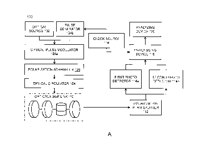
[0026] FIG. 1 A illustrates a block diagram 100 of a system for identification
of macro-bend losses
and differentiation of macro-bend losses from splice and connector losses in
at least one test fiber,
in accordance with an embodiment of the present disclosure. The identification
of the macro-bend
losses is based on characteristics of one or more macro-bends to display
significant changes in
Rayleigh scattering against different states of polarizations. The macro-bend
losses in optical fiber
links are characterized by a polarization dependent loss whereas the
attenuation or insertion losses
at splice joints and connectors are polarization independent. The polarization
dependent loss is
dependent primarily on the localized birefringence caused by the one or more
macro-bends in
optical fibers. In general, the polarization dependent loss is defined as peak
to peak power
throughput variation when input is exposed to every state of polarization. The
polarization
dependent loss is significantly dependent on one or more characteristics of
the fiber optic links. The
one or more characteristics include a number of the macro-bends, a number of
full circle loops in
each macro-bend, degree of bend radius and a wavelength of the optical carrier
signal.
Accordingly, the polarization dependent loss uniquely distinguishes the macro-
bends from one or
more splice joints and one or more connectors.
[0027] The block diagram 100 includes an optical source 102, an optical pulse
modulator 104a, a
pulse generator 104b, a polarization scrambler 106, an optical circulator 108,
an optical fiber link
110 and a polarization beam splitter 112. In addition, the block diagram 100
includes a first photo
8
CA 2962215 2017-03-27
detector 114a, a second photo detector 114b, a processing device 116, a clock
source 118 and an
analyzing device 120. The above arrangement facilitates calculation of
polarization dependent loss
along the optical fiber link 110 and identification of the one or more macro-
bends in the optical
fiber link 110. Moreover, the above arrangement facilitates differentiation
the one or more macro-
bends from the one or more splice joints and the one or more connector joints.
[0028] The measurement of the polarization dependent loss begins from
generation of required
optical signals. The optical source 102 generates optical signals. The optical
source 102 may be
any optoelectronic device for generation of the optical signals. In an
embodiment of the present
disclosure, the optical source 102 is a distributed feedback laser diode. The
optical source 102 may
be any standard laser source. Example of the standard laser source includes
but may not be limited
to a standard laser, a double hetero structure laser, separate confinement
laser (SCH) and a
distributed Bragg reflector laser. Moreover, the standard laser source may be
a quantum well laser,
a quantum dot laser, a quantum cascade laser and an external cavity laser. In
addition, the optical
source 102 may be any hybrid laser source. The optical source 102 generates
narrow band optical
signals at a wavelength operating in any one of the wavelength bands. Examples
of the wavelength
bands include an original band (hereinafter, "0-band"), an extended band
(hereinafter, "E-band"), a
short band (hereinafter, "S-band"), a conventional band (hereinafter, "C-
band"), a long band
(hereinafter, "L-band") and an ultra-long band (hereinafter, "L-band"). The
optical source 102
generates optical signals having an optical signal power in a range of 0 dBm
to 10 dBm.
[0029] The optical signals generated from the optical source 102 are pulse
modulated to obtain
modulated optical pulses. The optical signals are pulse modulated by utilizing
an optical
modulating device. The optical modulating device may any one of an acoustic
optic modulator
(AOM), an electro-absorption modulator (EAM) and an electro-optic modulator
(EOM). For
example, the electro-optic modulator is a LibNO3 based Mach Zehnder modulator.
[0030] In an embodiment of the present disclosure, the optical pulse modulator
104a modulates the
optical signals. The optical signals are characterized by a pre-defined
optical carrier wavelength, a
pre-defined optical peak power and a state of polarization. The optical
signals from the optical
source 102 are transferred to the optical pulse modulator 104a. The optical
pulse modulator 104a is
electrically linked to the pulse generator 104b. The pulse generator 104b
generates electrical pulses
for modulation of optical signals to the modulated optical pulses. The
electrical signals from the
pulse generator 104b have a pre-defined pulse width, a pre-defined pulse
repetition frequency and a
9
CA 2962215 2017-03-27
pre-defined electrical RF output power. The pre-defined electrical RF output
power corresponds to
power levels of the radio frequency electrical signals from the pulse
generator 104b. In an
embodiment of the present disclosure, the pulse generator 104b is electrically
linked to the optical
pulse modulator 104a. In another embodiment of the present disclosure, the
pulse generator 104b is
electrical linked to the optical source for direct pulse modulation (as shown
in FIG. 1B). The
electrical signals from the pulse generator 104b correspond to digital pulses
having the pre-defined
pulse width. The pre-defined pulse width lies in the range of picoseconds to
seconds. The optical
pulse modulator 104a uses the electrical signals to modulate the optical
signals to the modulated
optical pulses. The modulated optical pulses are characterized by a pre-
defined peak optical power,
a pre-defined optical carrier wavelength, the pre-defined optical pulse width
and a pre-defined
optical pulse repetition frequency.
[0031] The pre-defined optical carrier wavelength corresponds to wavelengths
of high frequency
optical signals generated from the optical source 102 for optical modulation.
The pre-defined
optical carrier wavelength lies in a band selected from a group of bands
comprising the 0-band, the
E-band, the S-band, the C-band, the L-band and the U-band. In an embodiment of
the present
disclosure, the 0 band is characterized by a wavelength in a range of 1260
nanometers to 1360
nanometers. In another embodiment of the present disclosure, the E-band is
characterized by a
wavelength in a range of 1360 nanometers to 1460 nanometers. In yet another
embodiment of the
present disclosure, the S-band is characterized by a wavelength in a range of
1460 nanometers to
1535 nanometers. In yet another embodiment of the present disclosure, the C-
band is characterized
by a wavelength in a range of 1535 nanometers to 1565 nanometers. In yet
another embodiment of
the present disclosure, the L-band is characterized by a wavelength in a range
of 1565 nanometers
to 1625 nanometers. In yet another embodiment of the present disclosure, the U-
band is
characterized by a wavelength in a range of 1625 nanometers to 1675
nanometers.
[0032] The optical pulse repetition frequency of the modulated optical pulses
is a rate at which
optical pulses in the modulated optical pulses are generated. The pre-defined
pulse-repetition
frequency lies in a range of Hz to MHz.
[0033] In another embodiment of the present disclosure, the optical source 102
modulates the
optical signal (as shown in FIG. 1B). The optical source 102 directly
generates modulated optical
pulses. The modulated optical pulses have the pre-defined optical carrier
wavelength, the pre-
defined optical peak power, the pre-defined optical pulse width, the pre-
defined optical pulse
CA 2962215 2017-03-27
repetition frequency and the state of polarization. The digital pulses from
the pulse generator 104b
are input to the optical source 102. The digital pulses directly modulate the
current in an active
region of the optical source 102. The output from the optical source 102 is
modulated optical pulses
with a peak optical power. The peak optical power lies in the range 0 dBm to
10 dBm and adjusted
by varying the bias current of the optical source 102. The width of the
modulated optical pulses can
be varied by controlling the width of digital pulses from the pulse generator
104b. The modulated
optical pulse width characterizes the minimum achievable system resolution.
[0034] In an embodiment of the present disclosure, the modulated optical
pulses are transmitted
from the optical pulse modulator 104a to the polarization scrambler 106
through one or more optical
links. In another embodiment of the present disclosure, the modulated optical
pulses are transmitted
directly from the optical source 102 to the polarization scrambler 106 through
one or more optical
links (as shown in FIG. 1B). The polarization scrambler 106 is an
optoelectronic device for varying
a normalized stokes vector of the state of polarization of the modulated
optical pulses over a
Poincare sphere. The polarization scrambler 106 scrambles the state of
polarization of the
modulated optical pulses to random states of polarization. Each random state
of polarization maps
to a single spherical coordinate on the Poincare sphere. The random state of
polarization of the
modulated optical pulses is scrambled at a pre-defined scrambling rate. The
pre-defined scrambling
rate lies in a range of Hz to KHz. The pre-defined scrambling rate is defined
by a scanning
frequency (FS). The scanning frequency (FS) is selectively preferred to be
less than or equal to a
reciprocal of a round trip time (T) of the modulated optical pulses to
traverse from a first end to a
second end of the optical fiber link 110.
[0035] The polarization scrambler 106 is linked through the one or more
optical links through an
optical circulator 108. The modulated optical pulses having the random states
of polarizations are
transmitted to the optical circulator 108 through the one or more optical
links. In an embodiment of
the present disclosure, the optical circulator 108 is a three port optical
device. The optical circulator
108 routes the modulated optical pulses through one or more ports. The one or
more ports of the
optical circulator 108 include a first port, a second port and a third port.
The first port of the optical
circulator 108 is associated with the polarization scrambler 106. The first
port of the optical
circulator 108 receives the modulated optical pulses from the polarization
scrambler 106 and routes
the modulated optical pulses to the second port. The second port of the
optical circulator 108 is
optically linked with the optical fiber link 110. The optical fiber link 110
includes one or more test
11
CA 2962215 2017-03-27
fibers, one or more fiber spools joined together through one or more splice
joints and/or one or
more connector joints. Each test fiber of the one or more test fibers is wound
around one or more
spools, looped around one or more mandrels of varying bend radii and stressed
for point bends.
Each spool holds one or more loops of the one or more test fibers. In
addition, the one or more
mandrels and point bends act as macro-bend, respectively in the optical fiber
link 110. The loss
events in each test fiber of the one or more test fibers is physically
characterized by the one or more
macro-bends, the one or more splice joints and the one or more connector
joints. The one or more
test fibers are geometrically characterized by a number of loops and a number
of macro-bends and
the like. The one or more macro-bends are characterized by the bend radius and
the number of
loops. The optical circulator 108 injects the modulated optical pulses in at
least one test fiber of one
or more test fibers. Each test fiber may be any standard single mode optical
fiber. The standard
single mode fiber is selected from a group of optical fibers. The group of
optical fibers includes but
may not be limited to a standard single mode fiber - G.652D fiber, a
dispersion shifted fiber - G.653
fiber, a cut-off shifted fiber - G.654 fiber, a non-zero dispersion shifted
fiber - G.655 fiber and a
bend-insensitive fiber - G.657 fiber. The optical circulator 108 is optically
linked to the polarization
scrambler 106.
[0036] The modulated optical pulses suffer from polarization dependent
Rayleigh scattering at each
macro-bend of the one or more macro-bends, Also, the modulated optical pulses
suffer from
polarization independent Rayleigh scattering at the one or more splice joints
and the one or more
connector joints. A fraction of the modulated optical pulses traverses back
from scattering in the
one or more macro-bends and travels back as back scattered optical pulses in
each test fiber of the
one or more test fibers. The back scattered optical pulses are routed from the
second port to the
third port of the optical circulator 108. The polarization beam splitter 112
is optically linked to the
third port of the optical circulator 108. The polarization beam splitter 112
receives the
backscattered optical pulses from the third port of the optical circulator
108. The backscattered
optical pulses are obtained after Rayleigh scattering in one or more macro-
bends of at least one test
fiber of the one or more test fibers. The polarization beam splitter 112 is a
passive optical device
for splitting optical signal to one or more components. The splitting of the
optical signal is based on
the state of polarization of the optical signal at an interface of the
polarization beam splitter 112.
The polarization beam splitter 112 splits the backscattered optical pulses in
a first optical
component and a second optical component. The first optical component and the
second optical
component are characteristically orthogonally polarized components of the
modulated optical
12
CA 2962215 2017-03-27
pulses. The polarization beam splitter 112 may be of any shape and size.
Examples of the shape of
polarization beam splitter 112 include but may not be limited to cube, plate,
prism and lateral
displacement. The first optical component is defined along a first principle
polarization state of
optical fiber and the second optical component is defined along a second
principle polarization state
of optical fiber. The first principle polarization state and the second
principle polarization of optical
fiber are orthogonal. For example, the first principle polarization state is
along an X axis and the
second principal polarization state is along a Y axis and moreover, the X axis
and the Y axis are
orthogonal to each other.
100371 The polarization beam splitter 112 is optically linked to the first
photo detector 114a and the
second photo detector 114b through a first optical link and a second optical
link. The first optical
link and the second optical link may be any discrete optical power transfer
mediums for transfer of
each component of the modulated optical pulses. The first photo detector 114a
and the second
photo detector 114b detect the first component and the second component of the
backscattered
optical pulses travelling through the first optical link and the second
optical link respectively. The
first photo detector 114a measures the first power of the first optical
component of the backscattered
optical pulses. The second photo detector 114b measures the second power of
the second optical
component of the backscattered optical pulses. The first photo detector 114a
and the second photo
detector 114b are optoelectronic devices for detection and measurement of
power levels of
incoming optical components.
100381 The precision and sensitivity of measurement of the first power and the
second power
depends on selection of the optical carrier wavelength of the optical signals.
The sensitivity of
measurement of the first power, the second power and the discrete values of
the polarization
dependent loss is increased by shifting the optical carrier wavelength from 0-
band to U-band. In an
embodiment of the present disclosure, the optical carrier wavelength is
shifted from the 0-band to
the U-band by changing the operating wavelength of the optical source 102.
Further, the first photo
detector 114a and the second photo detector 114b generate electrical signals
from the first
component and the second component of the back scattered optical pulses. The
generated electrical
signals are characterized by the pre-defined pulse repetition frequency of the
modulated optical
pulses. The first photo detector 114a and the second photo detector 114b are
electrically linked to
the processing device 116.
13
CA 2962215 2017-03-27
[0039] The electrical signals from the first photo detector 114a and the
second photo detector 114b
are transferred to the processing device 116. The processing device 116 is a
signal processing
device 116 for resampling and filtering out of band noise from the electrical
signals. In an
embodiment of the present disclosure, the processing device 116 is a digital
signal processor. In
another embodiment of the present disclosure, the processing device 116 is
digital filtering and
resampling circuit. The processing device 116 processes the received
electrical signals from the
first photo detector 114a and the second photo detector 114b. The electrical
signals correspond to
the backscattered optical pulses. The electrical signals are synchronously
resampled and filtered for
removal of out of band noise and an improvement in a signal to noise ratio.
Further, the processing
device 116 synchronously operates at a pre-defined clock repetition frequency
of an electrical clock
signal. The clock source 118 generates the electrical clock signal for
synchronizing operations of
the processing device 116 and the pulse generator 104b. The clock source 118
may be any
electronic device and may implement using any one of the crystal oscillator
and oscillator circuit to
generate the electrical clock signal. The electrical clock signal is
characterized by the pre-defined
clock repetition frequency. The clock source 118 is synchronously and
electrically linked to the
processing device 116 and the pulse generator 104b. The pre-defined clock
repetition frequency of
the processing device 116 matches corresponding clock repetition frequency of
the pulse generator
104b. The pre-defined clock repetition frequency is set and synchronized by
the clock source 118.
[0040] The electrical signals from the processing device 116 are transferred
to the analyzing device
120. The analyzing device 120 is electrically linked to the processing device
116. The analyzing
device 120 may be any instrument for graphical or non-graphical analysis of
the electrical signals.
Examples of the instrument includes but may not be limited to cathode ray
oscilloscopes, digital
signal oscilloscopes, mixed signal oscilloscopes, signal analyzers and
portable oscilloscopes. The
analyzing device 120 analyses the first power of the first optical component
and the second power
of the second optical component of the backscattered optical pulses. Further,
the analyzing device
120 calculates discrete values of polarization dependent loss as a function of
distance along a length
of the one or more test fibers. Each discrete value of the polarization
dependent loss is calculated
from a logarithm of a ratio of the first power corresponding to the first
optical component and the
second power corresponding to the second optical component. Each discrete
value of the
polarization dependent loss is a function of the bend radius, the number of
macro-bends and the pre-
defined optical carrier wavelength of the modulated optical pulses. Each
discrete value of the
polarization dependent loss is represented in decibels (dB).
14
CA 2962215 2017-03-27
Polarization Dependent Loss (PDL) = 20 * log10 (First Power of the first
optical
component/Second Power of the second optical component) dB
[0041] The analyzing device 120 identifies the macro-bend losses and
differentiates them from the
splice loss events and the connector loss events along the length of the one
or more test fibers. In
addition, the analyzing device 120 identifies the macro-bends by analyzing
peaks in one or more
plots of one or more traces of the discrete values of the polarization
dependent loss as the function
of distance. The one or more traces are generated from the discrete values of
the polarization
dependent loss as the function of the distance for each test fiber of the one
or more test fibers. Each
trace of the one or more traces corresponds to a segment of the length of the
one or more test fibers.
The polarization dependent loss is measured and traced as the function of the
distance along the
length of the one or more test fibers. The distance is dependent on selection
of the pre-defined
optical peak power and the pre-defined optical pulse width of the modulated
optical pulses. In an
embodiment of the present disclosure, the macro-bend loss events may be
manually identified and
differentiated from the splice loss events and the connector loss events. In
another embodiment of
the present disclosure, the macro-bend loss events may be automatically
identified and
differentiated from the splice loss events and the connector loss events.
Moreover, the macro-bend
losses are identified using a single wavelength of optical signals and system
complexity decreases
for the usage of single wavelength optical source. Each discrete value for the
polarization
dependent loss may be extrapolated to generate a continuous curve. The peaks
in each plot of the
one or more plots of the polarization dependent loss may correspond to the one
or more macro-
bends. Moreover, each peak value is characterized by the macro-bend loss
event. The macro-bend
losses may be automatically identified and differentiated from the splice
losses and connector losses
by utilizing programming software.
[0042] It may me noted that in FIG. 1 and FIG. 2, the optical circulator 108
is a three port optical
circulator; however, those skilled in the art would appreciate that more
number of optical ports may
be present in the optical circulator 108.
[0043] Figure 2 illustrates a flowchart 200 for identifying the macro-bend
losses and differentiating
them from the splice losses and the connector losses in the at least one test
fiber, in accordance with
various embodiments of the present disclosure. It may be noted that to explain
the process steps of
flowchart 200, references will be made to the system elements of the FIG. lA
and FIG. 1B. It may
also be noted that the flowchart 200 may have lesser or more number of steps.
CA 2962215 2017-03-27
[0044] The flowchart 200 initiates at step 202. Following step 202, at step
204, the optical pulse
modulator 104a generates the modulated optical pulses. The modulated optical
pulses have the pre-
defined optical carrier wavelength, the pre-defined optical peak power, the
pre- designated optical
pulse width and the pre-defined optical pulse repetition frequency. At step
206, the optical
circulator 108 injects the modulated optical pulses in each of the one or more
test fibers. At step
208, the polarization beam splitter 112 receives the backscattered optical
pulses. The backscattered
optical pulses correspond to the modulated optical pulses. The backscattered
optical pulses are
obtained after polarization dependent Rayleigh scattering in the one or more
macro-bends of at least
one test fiber of the one or more test fibers. At step 210, the polarization
beam splitter 112 splits the
backscattered optical pulses to the first optical component and the second
component. The first
optical component and the second optical component are characteristically
orthogonal polarized
components of the modulated optical pulses. At step 212, the first photo
detector 114a and the
second photo detector 114b measure the first power of the first optical
component and the second
power of the second optical component of the backscattered optical pulses
respectively. At step
214, the analyzing device 120 calculates the discrete values of the
polarization dependent loss as the
function of distance along the length of one or more test fibers. At step 216,
the analyzing device
120 enables identification of macro-bends along the length of one or more test
fibers by analyzing
peaks in one or more plots of one or more traces of the discrete values of the
polarization dependent
loss. The polarization dependent loss is measured as the function of the
distance. At step 218, the
analyzing device 120 differentiates loss events of one or more macro-bends
against the splice loss
and connector loss events along the length of the one or more test fibers. The
flowchart 200
terminates at step 220.
[0045] It may be noted that the flowchart 200 is explained to have above
stated process steps;
however, those skilled in the art would appreciate that the flowchart 200 may
have more/less
number of process steps which may enable all the above stated embodiments of
the present
disclosure.
[0046] The present disclosure provides several advantages over the prior art.
The present
disclosure substantially eliminate or at least partially address the
aforementioned problems in the
prior art, and provides a concrete solution for distinguishing macro-bend
losses from the splice
losses and connector losses. The measurement of polarization dependent loss as
a function of
distance facilitates in easier identification of segments and regions in the
optical fiber links having
16
CA 2962215 2017-03-27
macro-bends. Also, the method as described in the present disclosure helps in
visualization of
points of macro-bend and macro-bend losses as the function of distance along
the entire length of
the optical fiber link. The present disclosure enables plotting of traces of
the polarization dependent
losses for each segment of the optical fibers. The macro-bend losses are
identified using a single
wavelength of optical signals from the optical source which significantly
reduces the hardware
complexity and time for testing optical fiber links during installation and
production. The present
method also enables installation agencies to identify macro-bends in fiber
links currently installed in
long haul, metro and access communication networks. The present method
facilitates data
visualization of polarization dependent losses through real time plots and
traces for each segment of
the optical fiber link.
[0047] Modifications to embodiments of the present disclosure described in the
foregoing are
possible without departing from the scope of the present disclosure as defined
by the accompanying
claims. Expressions such as "including", "comprising", "incorporating",
"have", "is" used to
describe and claim the present disclosure are intended to be construed in a
non-exclusive manner,
namely allowing for items, components or elements not explicitly described
also to be present.
Reference to the singular is also to be construed to relate to the plural.
17