Note: Descriptions are shown in the official language in which they were submitted.
- 1 -
OPTICAL BEAM SCANNER
This application claims the benefit of U.S. provisional application No.
62/064,355, filed October
15, 2014.
BACKGROUND
Field
Embodiments of the invention relate to designs of a micro fabricated beam
scanning device and
its use in an arrayed format.
Background
Beam steering in imaging devices can be realized using various techniques
making use of electro
or thermo optical effects on chip or using mechanical scanning by moving
lenses or minors in
free space. A typical mechanism for beam steering uses a mirror for steering
the light coming
out of an optical waveguide and includes a collimating lens and a mirror
located at some distance
from the waveguide. The two-dimensional scanning mirror deflects the light
beam and projects it
over a sample.
The light propagation along optical waveguides patterned on chip occurs in-
plane. However
planar technologies commonly used for fabrication of integrated devices do not
allow for
fabrication of efficient collimating (or focusing) elements to obtain high
quality performance.
The lens is commonly located symmetrically with respect to the optical axis of
the waveguide. A
hybrid solution is often used to overcome this issue: a free space lens is
attached to the same
optical bench where the waveguide is fixed. However, aligning the free space
lens requires very
high precision in all three orthogonal directions on the order of 1 micron.
Many interferometry devices, such as optical coherence tomography (OCT)
systems, use
collimated light that is further directed to a focusing lens operated in
telecentric mode to make
the total optical path length indifferent to beam location on the imaged
sample. Using free space
optical elements can provide high quality performance; however it is
relatively bulky, requires
precise alignment, and does not leave much possibility for reduction of the
overall size of the
device.
Date recue/ date received 2022-02-18
CA 02964288 2017-04-11
WO 2016/059177 PCT/EP2015/073926
-2-
BRIEF SUMMARY
In the embodiments presented herein, device designs of a micro fabricated
optical beam scanner
that can be used with OCT applications are presented. The design also allows
for batch
fabrication of the device in order to form scanning arrays.
In an embodiment, a device is presented that includes a substrate having a
first surface and an
opposite, parallel second surface. The device includes a waveguide patterned
over the first
surface and configured to guide a beam of radiation along a length of the
waveguide. The device
also includes a facet located on the first surface and designed to reflect at
least a portion of the
beam of radiation at an angle that is substantially perpendicular to the first
surface. An optical
element is located on either the first surface or the second surface, and is
designed to receive the
reflected portion of the beam of radiation.
In another embodiment, a scanning device is presented having a substrate with
a first surface and
an opposite, parallel second surface. A region of the substrate includes the
first surface and the
opposite parallel second surface, and is defined via an etching process
through a thickness of the
substrate, where the region remains attached to the substrate via one or more
hinges. A
waveguide is patterned over the first surface of the region and guides a beam
of radiation along a
length of the waveguide. The scanning device includes a facet located on the
first surface of the
region. The facet is designed to reflect at least a portion of the beam of
radiation through the
region. An optical element is located on the second surface of the region, and
is designed to
receive the reflected portion of the beam of radiation.
In another embodiment, a scanning device is presented that includes a
plurality of individually
addressable elements formed from the same substrate. Each element of the
plurality of elements
includes a region of the substrate, a waveguide, a facet, and an optical
element. The region has a
first surface and an opposite parallel second surface, where the region is
defined via an etching
process through a thickness of the substrate, and where the region remains
attached to the
substrate via one or more hinges. The waveguide is patterned over the first
surface of the region
and guides a beam of radiation along a length of the waveguide. The facet is
located on the first
surface of the region and is designed to reflect at least a portion of the
beam of radiation through
the region. The optical element is located on the second surface of the
region, and is designed to
receive the reflected portion of the beam of radiation. Each element of the
plurality of elements
is designed to steer a corresponding beam of radiation via movement of a
corresponding region.
CA 02964288 2017-04-11
WO 2016/059177 PCT/EP2015/073926
-3-
BRIEF DESCRIPTION OF THE DRAWINGS/FIGURES
The accompanying drawings, which are incorporated herein and form a part of
the specification,
illustrate embodiments of the present invention and, together with the
description, further serve to
explain the principles of the invention and to enable a person skilled in the
pertinent art to make
and use the invention.
FIG. 1 illustrates a beam scanning device using free-space optics.
FIG. 2 illustrates a device for directing an optical beam, according to an
embodiment.
FIG. 3 illustrates a device for directing an optical beam, according to an
embodiment.
FIG. 4 illustrates a device for directing an optical beam, according to an
embodiment.
FIG. 5 illustrates a device for directing an optical beam, according to an
embodiment.
FIG. 6 illustrates a device for directing an optical beam, according to an
embodiment.
FIGs. 7A ¨ 7C illustrate various views of an optical beam scanner, according
to an embodiment.
FIG. 8 illustrates an optical beam scanner with two optical elements,
according to an
embodiment.
FIG. 9 illustrates a beam scanning device having a plurality of addressable
elements, according to
an embodiment.
FIG. 10 illustrates a block diagram of an interferometric system, according to
an embodiment.
FIG. 11 illustrates a simulated plot of reflectively vs. wavelength for
different i values, according
to an embodiment.
Embodiments of the present invention will be described with reference to the
accompanying
drawings.
DETAILED DESCRIPTION
Although specific configurations and arrangements are discussed, it should be
understood that
this is done for illustrative purposes only. A person skilled in the pertinent
art will recognize that
other configurations and arrangements can be used without departing from the
spirit and scope of
the present invention. It will be apparent to a person skilled in the
pertinent art that this invention
can also be employed in a variety of other applications.
It is noted that references in the specification to "one embodiment," "an
embodiment," "an
example embodiment," etc., indicate that the embodiment described may include
a particular
feature, structure, or characteristic, but every embodiment may not
necessarily include the
CA 02964288 2017-04-11
WO 2016/059177 PCT/EP2015/073926
-4-
particular feature, structure, or characteristic. Moreover, such phrases do
not necessarily refer to
the same embodiment. Further, when a particular feature, structure or
characteristic is described
in connection with an embodiment, it would be within the knowledge of one
skilled in the art to
effect such feature, structure or characteristic in connection with other
embodiments whether or
not explicitly described.
Embodiments herein relate to various designs of an optical beam scanner. Such
scanning devices
are useful for imaging applications that may acquire data by sweeping a beam
of radiation across
a sample. These imaging applications include, but are not limited to,
interferometry, Fourier
transform infrared microscopy (FTIR), confocal microscopy, and RAMAN
spectroscopy. Optical
coherence tomography (OCT) is one technique that is described herein and can
benefit from the
use of the embodied devices.
Herein, the terms "electromagnetic radiation," "light," "beam of radiation,"
and "optical beam"
are all used to describe the same electromagnetic signals propagating through
the various
described elements and systems.
The various device designs allow for the optical beam scanner to be fabricated
using standard
microfabrication techniques. In this way, bulk fabrication produces a high
number of scanning
devices with good uniformity and low cost. It should be understood that the
embodiments of the
present invention are not limited to specific fabrication steps taken to make
the devices. There
are many potential fabrication techniques known to one of ordinary skill in
the art that could be
used to ultimately fabricate the devices embodied herein.
One advantage to microfabrication is the monolithic integration of components
which leads to
better alignment and lower optical losses. FIG. 1 illustrates an example of a
beam scanning
device 100 that uses free-space optical elements to direct a beam towards a
sample. A substrate
102 includes a patterned waveguide 104 to guide a beam of light towards a lens
106. Lens 106 is
aligned off-chip with the output facet of waveguide 104. Lens 106 focuses the
light onto a
separate scanning mirror 108. An output beam of radiation 110 is reflected
from scanning mirror
108 towards sample 112. Scanning mirror 108 is coupled to an actuator in order
to laterally
move and/or tilt the angle of scanning mirror 108 in order to steer the
direction of beam of
radiation 110 towards sample 112. Alternatively light may be collimated by
lens 106, reflected
by mirror 108 and directed to a focusing lens operated in a telocentric mode
and located between
sample 112 and mirror 108.
Beam steering device 100 may produce a wide beam steering angle due to the
range of
movement afforded to scanning mirror 108. However, beam steering device 100
requires the use
CA 02964288 2017-04-11
WO 2016/059177 PCT/EP2015/073926
-5-
of free-space optical elements making miniaturization very difficult.
Additionally, each of the
optical elements must be precisely aligned which requires great skill and is
time consuming.
FIGs. 2-5 illustrate various embodiments of a device designed to direct a beam
of radiation. The
embodiments utilize the same basic concept of directing a beam of radiation at
an angle that is
substantially perpendicular to a surface of the substrate. However, the
embodiments differ in the
placement and formation of certain elements.
FIG. 2 illustrates a device 200 designed to direct a beam of radiation,
according to an
embodiment. Device 200 includes a substrate 202, a waveguide 204 that includes
a core layer
206 surrounded by cladding layers 208a and 208b, and an optical element 214. A
reflector 210 is
formed in-plane with waveguide 204 and is designed to reflect a beam of
radiation 212 towards
optical element 214.
Substrate 202 may be any suitable material that allows for surface and/or bulk
micromachining
patterning steps to be performed. In one example, substrate 202 is a
crystalline material such as
silicon, gallium arsenide, indium phosphide, etc. In other examples, substrate
202 is amorphous
such as glass or polysilicon. Core layer 206 of waveguide 204 may comprise a
material having a
higher refractive index than cladding layers 208a and 208b in order to confine
a beam of
radiation propagating through waveguide 204. Waveguide 204 may have a
crystalline structure
or be a polymer. Examples of waveguide 204 materials include, but are not
limited to, silicon,
silicon nitride, indium gallium arsenide, doped silicon, PMMA, Parylene, and
SU-8. In one
example, cladding layers 208a and 208b are silicon dioxide while both
substrate 202 and core
layer 206 are silicon. Waveguide 204 may be a strip waveguide, ridge
waveguide, or an optical
fiber laid across the surface of substrate 202.
Reflector 210 is placed a short distance from an end of waveguide 204,
according to an
embodiment. This distance cannot be too large, or else the beam of radiation
exiting from
waveguide 204 will spread too far and undesirable optical losses will occur.
In this embodiment,
both reflector 210 and waveguide 204 are patterned in-plane on a first surface
of substrate 202.
Reflector 210 may be designed to have a surface that is angled. For example,
reflector 210 may
have a surface that is angled at a substantially 45 degree angle with respect
to the first surface of
substrate 202. This angle causes the beam of radiation to be directed at an
angle that is
substantially perpendicular to the surface of substrate 202. In another
example, reflector 210 has
a surface that is angled at a substantially 54.74 degree angle with respect to
the first surface of
substrate 202. In the embodiment illustrated in FIG. 2, the light is reflected
up and away from
substrate 202 towards optical element 214.
CA 02964288 2017-04-11
WO 2016/059177 PCT/EP2015/073926
-6-
Reflector 210 may be formed from etching the layers that form waveguide 204,
according to an
embodiment. A wet anisotropic etchant may be used to strip away the material
along the crystal
planes to form the surface of reflector 210. The surface may be further
smoothed via an oxide
removal process by quickly exposing reflector 210 to another chemical etchant
such as
hydrofluoric acid (HF). Dry etching techniques may be employed as well for
creating the angled
surface of reflector 210. For example, reactive ion etching (RIE) using a grey-
scale type mask to
produce photoresist at varying heights can be used to produce non-planar
structures.
Optical element 214 is disposed over waveguide 204 and over a top surface of
substrate 202,
according to an embodiment. In this embodiment, optical element 214 is a lens.
The lens may be
designed to focus beam of radiation 212 or to collimate beam of radiation 212.
Optical element
214 may be manufactured using nano-imprint lithography or standard lithography
etching using a
grey-scale mask. Thermal reflow of a transparent polymer may also be used to
form the curved
lens shape. Optical element 214 may be fabricated using RIE directly in
substrate 202. The
advantage of using RIE may be realized when the substrate material has a high
refractive index
(e.g., material such as silicon, InP, etc.), thus the performance of the lens
depends much less on
the refractive index of the surrounding media. The curvature and position of
the focusing surface
of the lens may be adjusted so that the focal point and focal distance of the
lens achieve the
desired collimating or focusing performance. In one example, an intermediate
polymer layer is
introduced between optical element 214 and waveguide 204 in order to set a
lens working
distance. Optical element 214 may be subsequently coated with an anti-
reflective dielectric stack
to minimize light loss.
FIG. 3 illustrates another embodiment of a device 300 designed to direct a
beam of radiation.
Device 300 includes many of the same elements as device 200, including a
substrate 302, a
waveguide 304 with core layer 306 and cladding layers 306a and 306b, and a
reflector 310
positioned some distance away from an end of waveguide 304. Description of
these elements
will not be repeated for this embodiment.
Device 300 includes an optical element 314. In this embodiment, optical
element 314 is a mirror.
As such, optical element 314 receives beam of radiation 312 reflected from
reflector 310 and
reflects the beam of radiation down towards substrate 302. Optical element 314
may be curved
in such a way that beam of radiation 312 is collimated as it reflects away
from optical element
314. Optical element 314 may be formed using any of the same techniques
described above for
optical element 214. In order to penetrate substrate 302, substrate 302
includes a material that is
substantially transparent to a wavelength of beam of radiation 312. For
example, substrate 302
CA 02964288 2017-04-11
WO 2016/059177 PCT/EP2015/073926
-7-
may be silicon while beam of radiation 312 is in the infrared range. Examples
of infrared ranges
include near-infrared (800 nm ¨ 1.4 um), short-wave infrared (1.4 ¨ 3 pm), mid-
wave infrared (3
¨ 8 um), and long-wave infrared (15 ¨ 1000 um).
FIG. 4 illustrates another embodiment of a device 400 designed to direct a
beam of radiation.
Device 400 includes many of the same elements as device 200, including a
substrate 402, a
waveguide 404 with core layer 406 and cladding layers 408a and 408b, and a
reflector 410
positioned some distance away from an end of waveguide 404. However, reflector
410 is angled
such that a beam of radiation 412 is reflected downwards towards substrate
402, according to this
embodiment. Beam of radiation 412 traverses substrate 402 and is ultimately
received by optical
element 414. While waveguide 404 is patterned over a first surface of
substrate 402, optical
element 414 is coupled to an opposite, parallel surface of substrate 402. In
this way, both sides
of substrate 402 are utilized for directing and/or modulating beam of
radiation 412. In this
embodiment, optical element 414 is a lens similar to optical element 214.
Since beam of radiation 412 is reflected through substrate 402 before it
arrives at optical element
414, unwanted reflections of the light may occur at the surface of substrate
402. Additionally,
any reflected light from the surface of substrate 402 may couple back into
waveguide 404,
causing undesirable interference. According to an embodiment, device 400
includes an anti-
reflective (AR) coating 416. AR coating 416 may be applied and patterned on
the surface of
substrate 402 before the patterning of waveguide 404. AR coating 416 may be
patterned such
that it only exists beneath reflector 410, or it may encompass a larger area
on the surface of
substrate 402. In one example, AR coating 416 exists across the entire surface
of substrate 402.
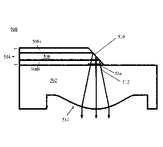
FIG. 5 illustrates another embodiment of a device 500 designed to direct a
beam of radiation.
Device 500 includes some of the same elements as device 200, such as substrate
502, waveguide
504 with core layer 506 and cladding layers 508a and 508b. In this embodiment,
reflector 510 is
formed from a facet at the end of waveguide 504. In this way, a beam of
radiation 512 is
reflected downwards towards substrate 502 before it has exited from waveguide
504.
An antireflective (AR) coating 516 is included at an interface between
waveguide 504 and
substrate 502, according to an embodiment. AR coating 516 may be patterned
such that it only
exists beneath reflector 510. In another example, AR coating 516 covers a
larger area on the
surface of substrate 502. AR coating 516 may exist across the entire surface
of substrate 502.
According to an embodiment, optical element 514 is formed in substrate 502 on
an opposite
surface from the surface where waveguide 504 is patterned. Optical element 514
may be
CA 02964288 2017-04-11
WO 2016/059177 PCT/EP2015/073926
-8-
designed to act as either a lens or a mirror. Optical element 514 may be
patterned using RIE
along with grey-scale lithography to create the non-uniform etch within
substrate 502.
FIG. 6 illustrates another embodiment of a device 600 designed to direct a
beam of radiation.
Device 600 is similar to device 500 and includes many of the same components
such as substrate
602, waveguide 604 having core layer 606 and cladding layers 608a and 608b and
reflector 610
to reflect a beam of radiation 612 towards an optical element 614. Two AR
coating layers 616a
and 616b are included within the path of beam of radiation 612 as it
propagates towards optical
element 614, according to an embodiment. AR coating 616a may be located at the
interface
between core layer 606 and cladding layer 608b while AR coating 616b may be
located at the
interface between cladding layer 608b and substrate 602.
According to another embodiment, AR coating 516 from Fig. 5 or AR coating
layers 616a and
616b from FIG. 6 are excluded from the design. In this case, a thickness t of
either cladding layer
508b or cladding layer 608b may be determined to substantially eliminate
backscattering of beam
of radiation 512/612 at the interface between cladding layer 508b/608b and
substrate 502/602.
In one example, cladding layer 508b/608b may comprise silicon dioxide with a
refractive index
of about ni = 1.4467, while core layer 506/606 and substrate 502/602 comprise
silicon with
refractive indices of no = 3.4434 and n2 = 3.4434, respectively. The
refractive indices are
provided for a given wavelength X = 1.32 ium. A reflectivity R at the silicon -
silicon dioxide -
silicon interfaces between core layer 506/606, cladding layer 508b/608b, and
substrate 502/602 is
provided by:
R = ri+ii1F2r1r2cos(24))
õ
1+1-1Q+2rii-2cos(2(p)
(1)
Where:
no¨ni
ri =
(2)
no+ni
r2 ni¨n2
(3)
ni+n2
2Tmit
=
(4)
The t values that maximize or minimize Eq. (1) can be obtained by solving for
dR/dt=0, which
results in:
CA 02964288 2017-04-11
WO 2016/059177
PCT/EP2015/073926
- 9 -
4. ( Ttnit) yields =
sin = 0 t = 1¨ (5)
4ni
where i is a positive integer greater than zero. For this particular
embodiment, R is
minimized for k=1.32 [tm when i is an even positive integer as illustrated in
FIG. 11.
Furthermore, it can be observed from FIG. 11 that the reflectivity peak is
broader when i
= 2 (i.e., t = 2./(20). Using this thickness (t = ?/(2n1)) for cladding layer
508b/608b may
enable low backscattering of the light in applications that require a wider
bandwidth.
FIGs. 2-6 illustrate embodiments for directing a beam of radiation through an
optical element.
These embodiments do not have the inherent ability to change the direction of
the output beam
without the use of some modulating element. Although some optical modulating
elements (e.g.,
thermal, acoustic, electric, etc.) may be included to steer the direction of
the output beam, the
range of angles that can be achieved are small compared to physical tilting or
movement of
certain elements.
FIGs. 7A ¨ 7C illustrate various views of a scanning device 700, according to
an embodiment.
FIG. 7A provides an isometric view, FIG. 7B provides a side view, and FIG. 7C
provides another
side view of scanning device 700. Scanning device 700 includes a substrate
702, a waveguide
704, and etched areas 706a and 706b which define a region 708 attached to
substrate 702 via
hinges 710a and 710b, according to an embodiment. Substrate 702 and waveguide
704 are
similar to those described above with reference to FIGs. 2-6. Scanning device
700 may also
include an antireflective (AR) coating between waveguide 704 and region 708.
In the embodiment shown, a reflector 712 is included as a facet at the end of
waveguide 704,
which is patterned over region 708. Reflector 712 receives a beam of radiation
714 propagating
along a length of waveguide 704 and reflects beam of radiation 716 through
region 708 and
towards an optical element 718 disposed on an opposite, parallel surface of
region 708. Reflector
712 may also be included some distance away from waveguide 704 as previously
described with
respect to any of FIGs. 2-4.
.. Etched regions 706a and 706b penetrate through the thickness of substrate
702, such that region
708 is only suspended in place via hinges 710a and 710b, according to an
embodiment. Etched
regions 706a and 660b may be formed using a dry chemical etching process such
as RIE, deep
reactive ion etching (DRIE), inductively coupled plasma (ICP) etching, Xenon
Difluoride (XeF2)
etching etc. or using a wet chemical etching process such as potassium
hydroxide (KOH) etching,
or tetramethylammonium hydroxide (TMAH) etching.
CA 02964288 2017-04-11
WO 2016/059177 PCT/EP2015/073926
- 10 -
Optical element 718 may be a lens or mirror as discussed previously, and may
be formed via any
of the methods already described in the embodiments illustrated in FIGs. 2-6.
Optical element
718 may be used to either focus or collimate beam of radiation 716. In the
embodiment
illustrated in FIG. 7B, optical element 718 is a lens patterned in the bottom
surface of region 708.
In this way, reflector 712 is located on a top surface of region 708 while
optical element 718 is
on an opposite, parallel bottom surface of region 708.
Region 708 may be attached to substrate 702 via any number of hinges. For
example, only a
single hinge may be used to attached region 708 to substrate 702. In another
example, multiple
hinges located along one side of region 708 may be used. In yet another
example, a hinge may
be placed along each side or each corner of region 708. Waveguide 704 may be
pattered to
extend along the surface of one of the hinges such that reflector 712 is
located over region 708.
In the embodiment illustrated in FIG. 7A, waveguide 704 is patterned over
hinge 710b.
Region 708 is able to rotate about an axis that passes through hinges 710a and
710b, according to
an embodiment. This rotation is illustrated in FIG. 7C. Based on the stiffness
and size of hinges
710a and 710b, region 708 may rotate up to an angle 0 with respect to the top
surface of region
708. In one example, region 708 may rotate up to 10 degrees. In another
example region 708
may rotate up to 20 degrees. Region 708 may be capable of rotating about any
number of axes
passing through any number of hinges that couple region 708 to substrate 702.
In an
embodiment, both the source of the beam of radiation (reflected from reflector
712) and optical
element 718 are rotated together as a rigid structure thus providing uniform
aberration level
operation throughout the scanning range. In another embodiment, region 708 may
be laterally
displaced with respect to an axis that passes through hinges 710a and 710b.
The rotation of region 708 may be performed via a variety of well-known
techniques in the field
of Microelectromechanical systems (MEMS). For example, region 708 may be
electrically
isolated from a portion of substrate 708, while a first potential is applied
to region 708 and a
different potential is applied to the portion of substrate 708 in proximity to
region 708. The
electrostatic interaction caused by the difference in potential causes a
movement in region 708.
Capacitance pull-in effects may also be leveraged to cause a rotation of
region 708. Piezoelectric
materials (such as PZT or PVDF) may also be employed to cause rotation of
region 708. In
another embodiment, electromagnetic actuation can be used if an electric coil
is fabricated on
region 708. Electric current flowing through the coil excites a magnetic field
which interacts with
a magnetic field induced in proximity of region 708 thus producing
rotation/displacement of
region 708.
CA 02964288 2017-04-11
WO 2016/059177 PCT/EP2015/073926
-11-
FIG. 8 illustrates another embodiment of a scanning device 800. Scanning
device 800 includes
many similar features as scanning device 800, such as substrate 802, waveguide
804, reflector
806, and region 808 supported by hinges 810a and 810b. Scanning device 800
includes an
optical element 812 formed in the lower surface of region 808 via, for
example, micromachining
techniques. Optical element 812 may be a lens formed from the same silicon
that makes up the
rest of region 808, while a second optical element 814 is coupled to an outer
surface of optical
element 812. Second optical element 814 may have a different refractive index
than optical
element 812. For example, second optical element 814 may be a polymer while
optical element
812 is a silicon lens.
FIG. 9 illustrates a scanning array 900 that includes a plurality of
individually addressable
elements 902, according to an embodiment. Each addressable element 902 may
function
substantially similar to scanning device 700 as described with respect to
FIGs. 7A ¨ 7C. As
such, each addressable element 902 may be designed to steer a corresponding
beam of radiation
emanating from the corresponding addressable element. Although FIG. 9
illustrates a single row
of addressable elements 902, it should be understood that any arrangement of
addressable
elements is possible, such as a matrix having any number of rows and columns.
By leveraging
bulk fabrication techniques, the plurality of addressable elements may be made
in a quick and
relatively inexpensive manner.
Scanning array 900 may be used for numerous imaging applications, including
OCT. As such,
an optical source 904 may be coupled to a multiplexing unit 906 to deliver the
various beams of
radiation to each addressable element 902. Optical source 904 may include one
or more lasers,
one or more light emitting diodes, or one or more gas discharge sources. In
one example, optical
source 904 includes a swept laser source to output a range of different
wavelengths.
Multiplexing unit 906 may include associated electronics that provide control
signals to various
modulating elements of multiplexing unit 906 in order to direct light through
various waveguides
that ultimately lead to each of addressable elements 902. Multiplexing unit
906 may use any
multiplexing method that allows for the separation of the light directed to
each addressable
element 902. One such multiplexing method is time-domain multiplexing, in
which multiplexing
unit 906 switches between different output waveguides in a controlled manner,
so that at a given
time only one associated waveguide is active. Another suitable multiplexing
method is
frequency-domain multiplexing, in which light traversing each of the
waveguides is modulated in
such a way that the time-frequency behavior of signals corresponding to
different waveguides
can be differentiated by a processing device. Coherence-domain multiplexing
may also be used
CA 02964288 2017-04-11
WO 2016/059177 PCT/EP2015/073926
- 12 -
in multiplexing unit 906, by introducing a different group delay to the light
traversing each
waveguide, so that the signals corresponding to different waveguides appear at
different
coherence positions and can be therefore differentiated by a processing
device. In an
embodiment, these methods are non-exclusive and can be combined in order to
find the best
design compromise. Based on the multiplexing method used, multiplexing unit
906 may be a
passive element or electrically driven. Some of the multiplexing methods, like
coherence-
domain multiplexing, do not require any electrical actuation of multiplexing
unit 906. Thus, in
an embodiment, implementations based on coherence-domain multiplexing do not
require
electrical transmission media for control signals.
A control circuit 908 may also be included as part of scanning array 900.
Control circuit 908
provides electrical signals to each of addressable elements 902. These
electrical signals cause the
moveable regions of the addressable elements to rotate, according to an
embodiment. Control
circuit 908 may be designed such that each of the addressable elements 902
rotates in unison.
Control circuit 908 may send different signals to each addressable element 902
such that the
rotation of each element is different. Control circuit 908 may receive inputs
from another
processing unit or directly from a user to select which addressable elements
are used.
The array of scanning devices in combination with appropriately working
integrated optics may
permit reaching a high scanning rate over an extensive field of view with a
high signal-to-noise
ratio (SNR) even on Time Domain OCT systems. In the case of swept-source
systems, this
solution can increase scanning speed as each individual addressable element
902 may be
designed with a large resonant and operating frequency, providing a better
performance than
larger bulk-optics constructions.
Each individually addressable element 902 may be associated with its own
interferometer for
performing OCT imaging, according to an embodiment. In another example, the
beams of
radiation from each addressable element 902 are multiplexed, such that they
can each be used
within the same interferometer.
An interferometer arrangement that can be used to perform OCT on a sample is
illustrated in
FIG. 10. OCT system 1001 includes an optical source 1002, a splitting element
1004, a sample
arm 1006, a reference arm 1008, a delay unit 1012, and a detector 1014. Delay
unit 1012 may
include various light modulating elements. These modulating elements may
perform phase
and/or frequency modulation to counteract undesired optical effects in the
light, and to select one
or more depths of sample 1010 to be imaged. The use of the term "light" may
refer to any range
CA 02964288 2017-04-11
WO 2016/059177 PCT/EP2015/073926
- 13 -
of the electromagnetic spectrum. In an embodiment, the term "light" refers to
infrared radiation
at a wavelength of about 1.3 um.
In the embodiment shown, delay unit 1012 is located within reference arm 1008.
However, it
should be understood that delay unit 1012 may instead be located in sample arm
1006.
Alternatively, various elements of delay unit 1012 may be present in both
sample arm 1006 and
reference arm 1008. For example, elements of delay unit 1012 that introduce a
variable delay to
the light may be located in sample arm 1006, while elements that modulate
different polarization
modes of the light may be located in reference arm 1008. In one example,
sample arm 1006 and
reference arm 1008 are optical waveguides, such as patterned waveguides or
optical fibers. In an
embodiment, all of the components of OCT system 1001 are integrated onto a
planar lightwave
circuit (PLC). In another embodiment, at least the components within delay
unit 1012 are
integrated on the same substrate of a PLC. Other implementations may be
considered as well,
such as, for example, fiber optic systems, free-space optical systems,
photonic crystal systems,
etc. The various optical components, such as splitting element 1004, sample
arm 1006, reference
arm 1008, and delay unit 1012, may be integrated on the same substrate as
multiplexing unit 804.
It should be understood that OCT system 1001 may include any number of other
optical elements
not shown for the sake of clarity. For example, OCT system 1001 may include
mirrors, lenses,
gratings, splitters, micromechanical elements, etc., along the paths of sample
arm 1006 or
reference arm 1008.
Splitting element 1004 is used to direct light received from optical source
1002 to both sample
arm 1006 and reference arm 1008. Splitting element 1004 may be, for example, a
bi-directional
coupler, an optical splitter, or any other modulating optical device that
converts a single beam of
light into two or more beams of light.
Light that travels down sample arm 1006 ultimately impinges upon sample 1010.
In an
embodiment, sample arm 1006 includes a waveguide that guides the light towards
one or more of
addressable elements 902. Sample 1010 may be any suitable sample to be imaged,
such as tissue.
The light scatters and reflects back from various depths within sample 1010,
and the
scattered/reflected radiation is collected back into sample arm 1006. In
another embodiment, the
scattered/reflected radiation is collected back into a different waveguide
than the transmitting
waveguide. The scan depth may be chosen via the delay imposed on the light
within delay unit
1012.
Light within sample arm 1006 and reference arm 1008 is recombined before being
received at
detector 1014. In the embodiment shown, the light is recombined by splitting
element 1004. In
CA 02964288 2017-04-11
WO 2016/059177 PCT/EP2015/073926
- 14 -
another embodiment, the light is recombined at a different optical coupling
element than splitting
element 1004. Detector 1014 may include any number of photodiodes, charge-
coupling devices,
and/or CMOS structures to transduce the received light into an electrical
signal. The electrical
signal contains depth-resolved optical data related to sample 1010 and may be
received by a
processing device for further analysis and signal processing procedures. As
used herein, the term
"depth-resolved" defines data in which one or more portions of the data
related to specific depths
of an imaged sample can be identified.
Optical source 1002 may include one or more light emitting diodes (LEDs) or
laser diodes. For
example, LEDs may be used when performing time domain and/or spectral domain
analysis,
while tunable lasers may be used to sweep the wavelength of the light across a
range of
wavelengths.
OCT system 1001 is illustrated as an interferometer design similar to a
Michelson interferometer,
according to an embodiment. However, other interferometer designs are possible
as well,
including Mach-Zehnder or Mireau interferometer designs.
It is to be appreciated that the Detailed Description section, and not the
Summary and Abstract
sections, is intended to be used to interpret the claims. The Summary and
Abstract sections may
set forth one or more but not all exemplary embodiments of the present
invention as
contemplated by the inventor(s), and thus, are not intended to limit the
present invention and the
appended claims in any way.
Embodiments of the present invention have been described above with the aid of
functional
building blocks illustrating the implementation of specified functions and
relationships thereof.
The boundaries of these functional building blocks have been arbitrarily
defined herein for the
convenience of the description. Alternate boundaries can be defined so long as
the specified
functions and relationships thereof are appropriately performed.
The foregoing description of the specific embodiments will so fully reveal the
general nature of
the invention that others can, by applying knowledge within the skill of the
art, readily modify
and/or adapt for various applications such specific embodiments, without undue
experimentation,
without departing from the general concept of the present invention.
Therefore, such adaptations
and modifications are intended to be within the meaning and range of
equivalents of the disclosed
embodiments, based on the teaching and guidance presented herein. It is to be
understood that
the phraseology or terminology herein is for the purpose of description and
not of limitation, such
that the terminology or phraseology of the present specification is to be
interpreted by the skilled
artisan in light of the teachings and guidance.
CA 02964288 2017-04-11
WO 2016/059177 PCT/EP2015/073926
- 15 -
The breadth and scope of the present invention should not be limited by any of
the above-
described exemplary embodiments, but should be defined only in accordance with
the following
claims and their equivalents.