Note: Descriptions are shown in the official language in which they were submitted.
CA 2964695 2017-04-19
ANTENNA APERTURE TUNING AND RELATED METHODS
TECHNICAL FIELD
[0001] This
disclosure relates to frequency tunable antennas in wireless
communication systems and, more specifically, to antenna aperture tuning and
related
methods.
BACKGROUND
[0002] Current
mobile wireless communications devices, such as smartphones,
tablets and the like, may need to operate at a variety of frequency bands to
support
roaming or multiple radio access technologies, for example, operating at Long
Term
Evolution (LTE) bands, Global System for Mobile Communications (GSM) bands,
Universal Mobile Telecommunications System (UMTS) bands, and/or wireless local
area network (WLAN) bands, covering frequency ranges such as 700-960 MHz, 1710-
2170 MHz, and 2500-2700 MHz. In some cases, a device may need to support
carrier
aggregation so that the device can aggregate multiple frequency carriers to
increase data
transmission rates. Frequency tunable antennas can be used in mobile devices
to support
operations at different frequencies.
DESCRIPTION OF DRAWINGS
[0003] FIG. 1
shows an example mobile wireless communications device,
according to some implementations.
[0004] FIG. 2A
illustrates aperture tuning for a planar inverted "F" antenna
(PIFA), according to some implementations.
[0005] FIG. 2B
illustrates aperture tuning for an inverted "L" antenna, according
to some implementations.
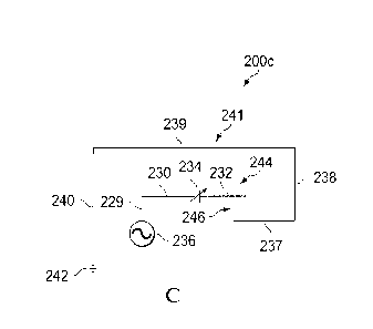
[0006] FIG. 2C
illustrates aperture tuning for a parasitic monopole antenna,
according to some implementations.
[0007] FIG. 3A
illustrates a frequency tunable PIFA using impedance tuning,
according to some implementations.
[0008] FIG. 3B
illustrates a first example of impedance tuning for a PIFA,
according to some implementations.
[0009] FIG. 3C
illustrates a second example of impedance tuning for a PIFA,
according to some implementations.
CA 2964695 2017-04-19
100 1 01 FIG. 3D
illustrates a third example of impedance tuning for a PIFA,
according to some implementations.
[0011] FIG. 4A
illustrates using impedance tuning to enable frequency tuning
for a parasitic monopole antenna, according to some implementations.
[0012] FIG. 4B
illustrates a first example of impedance tuning for a parasitic
monopole antenna, according to some implementations.
[0013] FIG. 4C
illustrates a second example of impedance tuning for a parasitic
monopole antenna, according to some implementations.
[0014] FIG. 4D
illustrates a third example of impedance tuning for a parasitic
to monopole antenna, according to some implementations.
[0015] FIG. 5
illustrates an example top patch of a PIFA, according to some
implementations.
[0016] FIG. 6
illustrates a MIMO antenna assembly, according to some
implementations.
[0017] FIG. 7 illustrates
example components of a mobile wireless
communications device that may be used in accordance with the described
antenna
assemblies.
[0018] FIG. 8
is a flowchart illustrating an example method for aperture
tuning, according to some implementations.
[0019] Like reference
numbers and designations in the various drawings indicate
like elements.
DETAILED DESCRIPTION
[0020] The
present disclosure is directed to antenna aperture tuning and related
methods. In particular, frequency tunable antennas are implemented using
tunable
circuits in antenna assemblies. For example, aperture tuning may adjust an
antenna
resonant frequency by changing an electrical length of a radiating element of
the
antenna. In some implementations, impedance tuning may adjust an antenna
resonant
frequency by changing a loading impedance between a radiating element of the
antenna
and a ground. In some cases, two antennas of a multiple-input multiple-output
(MIMO)
system can be coupled by a tunable circuit to reduce a correlation between
radiating
patterns of the two antennas and hence optimize a MIMO system performance.
[0021] In some
implementations, an antenna assembly can include an antenna
2
CA 2964695 2017-04-19
feed, and a first radiating element connecting to the antenna feed, where the
first
radiating element includes a proximal radiating segment and a distal radiating
segment.
The antenna assembly can also include a tunable circuit coupling the proximal
radiating
segment and the distal radiating segment. The tunable circuit is configured to
adjust a
resonant frequency of the antenna assembly to a predetermined frequency. The
tunable
circuit can include a tunable capacitor, where the tunable capacitor can have
a
substantially continuous range of capacitance. The tunable circuit can be
adjusted to
modify an electrical length of the first radiating element, and modifying the
electrical
length changes the resonant frequency of the antenna assembly. The
predetermined
frequency can be a frequency in a cellular band, Global Positioning System
(GPS) band,
Personal Communications Service (PCS) band, Long Term Evolution (LTE) band, or
wireless local area network (WLAN) band. The antenna assembly can further
include a
second radiating element capacitively coupled to the first radiating element
through a
gap and the second radiating element can connect to a ground. The antenna
assembly
can also include a shorting pin that connects the first radiating element to a
ground.
[0022] In some implementations, an antenna assembly can include a first
radiating element, and a tunable circuit connecting the first radiating
element to a
ground. The tunable circuit can be configured to adjust a resonant frequency
of the
antenna assembly to a predetermined frequency. The tunable circuit can include
at least
a tunable capacitor and the tunable capacitor can have a substantially
continuous range
of capacitance. The tunable circuit can be adjusted to modify a loading
impedance
between the first radiating element and the ground, and modifying the loading
impedance changes the resonant frequency of the antenna assembly. The
predetermined
frequency can be a frequency in a cellular band, GPS band, PCS band, LTE band,
or
WLAN band. The antenna assembly can further include a second radiating element
capacitively coupled to the first radiating element through a gap and the
second radiating
element connected to an antenna feed. In some cases, the first radiating
element can
connect to an antenna feed.
[0023] In some
implementations, a multiple-input multiple output (MIMO)
antenna assembly can include a first antenna assembly and a second antenna
assembly.
The first antenna assembly includes a first radiating element including a
first proximal
radiating segment and a first distal radiating segment. The first antenna
assembly also
includes a first tunable circuit coupling the first proximal radiating segment
and the first
3
CA 2964695 2017-04-19
distal radiating segment and configured to adjust a resonant frequency of the
first
antenna assembly to a predetermined frequency. The second antenna assembly
includes
a second radiating element including a second proximal radiating segment and a
second
distal radiating segment. The second antenna assembly also includes a second
tunable
circuit coupling the second proximal radiating segment and the second distal
radiating
segment and configured to adjust a resonant frequency of the second antenna
assembly
to the predetermined frequency. The MIMO antenna assembly also includes a
third
tunable circuit connecting the first antenna assembly and the second antenna
assembly
and configured to modify a correlation between radiating patterns of the first
antenna
to assembly and
the second antenna assembly. At least one of the first, second or third
tunable circuit includes a tunable capacitor, and the tunable capacitor has a
substantially
continuous range of capacitance. The third tunable circuit can be adjusted to
change a
coupling impedance between the first antenna assembly and the second antenna
assembly, changing the coupling impedance can modify current distribution
between
the first antenna assembly and the second antenna assembly, and modifying the
current
distribution can adjust the correlation between radiating patterns of the
first antenna
assembly and the second antenna assembly. The predetermined frequency can be a
frequency in a cellular band, GPS band, PCS band, LTE band, or WLAN band.
[0024] In some
implementations, an antenna assembly resonates at a first
resonant frequency. The antenna assembly can include a radiating element and a
tunable
circuit coupled to the radiating element. The tunable circuit can be adjusted
based on a
second resonant frequency. The antenna assembly can modify an electrical
length of
the radiating element based on the adjusted tunable circuit such that the
antenna
assembly resonates at the second resonant frequency. The radiating element can
connect
to an antenna feed and include a proximal radiating segment and a distal
radiating
segment. The tunable circuit can be coupled to the proximal radiating segment
and the
distal radiating segment and configured to adjust the electrical length of the
radiating
element.
[0025] In some
implementations, a non-transitory computer readable medium
includes instructions which, when executed, cause an antenna assembly to
resonate at a
first resonant frequency. The antenna assembly includes a radiating element
and a
tunable circuit coupled to the radiating element. The instructions can cause
the tunable
circuit to be adjusted based on a second resonant frequency. The instructions
can also
4
CA 2964695 2017-04-19
cause the antenna assembly to modify an electrical length of the radiating
element based
on the adjusted tunable circuit such that the antenna assembly resonates at
the second
resonant frequency. The radiating element can connect to an antenna feed and
include
a proximal radiating segment and a distal radiating segment. The tunable
circuit can be
coupled to the proximal radiating segment and the distal radiating segment and
configured to adjust the electrical length of the radiating element.
[0026] The
subject matter described herein may provide one or more
advantages. The described antenna assembly can resonate at different
frequencies to
support operations at different frequency bands or carrier aggregation. The
described
to antenna
assembly can also provide a large operating frequency range and a high antenna
efficiency to accommodate a wide range of power amplifier characteristics. The
described MIMO antenna assembly can reduce a correlation between radiating
patterns
of the two antennas such that the MIMO system can provide a high data rate. In
the
context of the current invention disclosure, the terms "antenna" and "antenna
assembly"
are considered technically equivalent unless indicated otherwise.
[0027] FIG. 1
shows an example mobile wireless communications device 100,
according to some implementations. The mobile wireless communications device
100
illustratively includes a portable housing 31 and a printed circuit board
(PCB) 32 affixed
to the portable housing 31. The portable housing 31 can have an upper portion
and a
lower portion. As illustrated, a wireless transceiver 33 is affixed to the PCB
32. In some
cases, the PCB 32 may be replaced by or used in conjunction with a metal
chassis or
other substrate. The PCB 32 may also include a conductive layer (not shown)
defining
a ground plane. A satellite positioning signal receiver 34 can also be affixed
to the PCB
32. The satellite positioning signal receiver 34 may be a Global Positioning
System
(GPS) satellite receiver. The exemplary device 100 can also include a display
35 which
may be, for example, a full graphic liquid-crystal display (LCD). The device
30 further
illustratively includes an antenna assembly 40 affixed to the upper portion of
the PCB
32. In some implementations, the antenna assembly 40 can include a frequency
tunable
antenna or MIMO antenna so that the device 100 can operate under multiple
frequencies.
A controller 38 or processor may also be affixed to the PCB 32. The controller
38 may
be communicatively coupled to the other components, for example, the antenna
assembly 40, the satellite positioning signal receiver 34, and the wireless
transceiver 33
to coordinate and control operations of the mobile wireless communications
device 100.
5
CA 2964695 2017-04-19
In some implementations, the mobile wireless communications device 100 may
include
multiple PCBs, such as two PCBs connected by a connecting flex. For example,
for a
MIMO antenna system with two antennas, a first antenna can be on a first PCB
at the
upper portion of the portable housing 31 and a second antenna can be on a
second PCB
at the lower portion of the portable housing 31.
[0028] FIGS. 2A-
2C illustrate frequency tunable antennas using aperture tuning.
FIG. 2A illustrates aperture tuning for a planar inverted "F" antenna (PIFA)
200a,
according to some implementations. The antenna 200a resembles an inverted
letter "F"
explaining the PIFA name but may have other configurations without departing
from
the scope of the disclosure. The antenna 200a has a radiating element 214
including a
proximal radiating segment 202 and a distal radiating segment 204 coupled by a
tunable
capacitor 206. The proximal radiating segment 202 has two ends, one end
connecting
to the tunable capacitor 206 and the other end connecting to a shorting pin
208 that
connects the radiating element 214 to a ground 210. The proximal radiating
segment
202, at a point between its two ends, further connects to antenna feed 212. In
some
cases, the antenna feed 212 can be an AC voltage source, such as a radio
frequency (RF)
signal. The tunable capacitor 206 can have a continuous range of capacitance
or a
substantially continuous range of capacitance. In some implementation, the
capacitance
of the tunable capacitor can be adjusted by changing the DC voltage applied
across the
tunable capacitor. Adjusting the capacitance of the tunable capacitor 206 can
change an
electrical length of the radiating element 214. An electrical length of an
antenna
component can be similar to, or different from a physical length. The
electrical length
can be effectively adjusted by using circuit components. Adjusting the
electrical length
of the radiating element 214 can change the resonant frequency of the antenna
200a. In
some implementations, as will be discussed in FIG. 5, PIFA 200a can be formed
by a
radiating patch that includes the radiating element 214.
[0029] FIG. 2B
illustrates aperture tuning for an inverted "L" antenna 200b,
according to some implementations. The antenna 200b resembles an inverted
letter "L"
explaining the name but may have other configurations without departing from
the scope
of the disclosure. The antenna 200b has a radiating element 228 including a
proximal
radiating segment 220 and a distal radiating segment 222 coupled by a tunable
capacitor
224, and a third radiating segment 225. The proximal radiating segment 220 and
the
third radiating segment 225 form an L-shape. The third radiating segment 225
connects
6
CA 2964695 2017-04-19
to antenna feed 226. The tunable capacitor 224 can have a continuous range of
capacitance or a substantially continuous range of capacitance. Adjusting the
capacitance of the tunable capacitor 224 can change an electrical length of
the radiating
element 228 and adjust the antenna resonant frequency.
[0030] FIG. 2C
illustrates aperture tuning for a parasitic monopole antenna
200c, according to some implementations. The antenna 200b has a first
radiating
element 244 including a proximal radiating segment 230 and a distal radiating
segment
232 coupled by a tunable capacitor 234, and a third radiating segment 229. The
proximal
radiating segment 230 and the third radiating segment 229 form an L-shape but
may
have other configurations without departing from the scope of the disclosure.
The third
radiating segment 229 connects to antenna feed 236. The antenna 200c also has
a second
radiating element 241 including four connected radiating segments, 237, 238,
239, 240,
with segments 237, 238, 239 forming a U-shape, and segments 239 and 240
forming an
L-shape. The segment 240 connects to a ground 242. The second radiating
element 241
is capacitively coupled to the first radiating element 244, through a gap 246.
The tunable
capacitor 234 can have a continuous range of capacitance or a substantially
continuous
range of capacitance. Adjusting the capacitance of the tunable capacitor 234
can change
an electrical length of the first radiating element 244 and adjust the antenna
resonant
frequency.
[0031] In some
implementations, tunable capacitors 206, 224 and 234 each can
be replaced by a tunable circuit which may include various tunable and non-
tunable
circuit components such as capacitors and/or inductors and any combination of
these
circuit components. As will be appreciated by those skilled in the art,
capacitance values
of tunable capacitors 206, 224, and 234 may be determined based on a desired
or
predetermined resonant frequency or frequency range, and, in some
implementations,
may be derived by simulation hardware and/or programs. The desired or
predetermined
resonant frequency or frequency range can be a frequency or frequency range in
a
cellular band, GPS band, PCS band, LTE band, WLAN band, or other bands.
[0032] FIG. 3A
illustrates a frequency tunable PIFA 300a using impedance
tuning, according to some implementations. The antenna 300a includes a
radiating
element 302 with one end connecting to a shorting pin 303. The shorting pin
303
connects to a ground 308 through a tunable circuit 304. The radiating element
302, at a
point between its two ends, connects to antenna feed 306. Adjusting the
tunable circuit
7
CA 2964695 2017-04-19
304 can change a loading impedance between the shorting pin 303 and ground 308
and
hence change the antenna resonant frequency. The tunable circuit 304 can
include
various tunable and non-tunable circuit components, such as capacitors and/or
inductors
and any combination of these circuit components. In some implementations,
adjusting
the tunable circuit 304 includes adjusting the capacitance of the tunable
capacitor in the
tunable circuit 304.
[0033] FIGS. 3B-
3D illustrate examples of the tunable circuit in FIG. 3A. FIG.
3B illustrates a first example of impedance tuning for a PIFA 300b, according
to some
implementations. The antenna 300b has a tunable circuit 316 including a
tunable
capacitor in series with a fixed (i.e., non-tunable) inductor. FIG. 3C
illustrates a second
example of impedance tuning for a PIFA 300c, according to some
implementations. The
antenna 300c has a tunable circuit 318 including a tunable capacitor in
parallel with a
fixed inductor. FIG. 3D illustrates a third example of impedance tuning for a
PIFA
300d, according to some implementations. The antenna 300d has a tunable
circuit 320
including a first tunable capacitor in parallel with a second tunable
capacitor and a fixed
inductor connected in series. The tunable capacitors in tunable circuits 316,
318, and
320 can have a continuous range of capacitance or a substantially continuous
range of
capacitance. As will be appreciated by those skilled in the art, capacitance
values of
tunable capacitors in tunable circuits 316, 318, and 320 may be determined
based on a
desired or predetermined resonant frequency or frequency range, and, in some
implementations, may be derived by simulation hardware and/or programs. The
desired
or predetermined resonant frequency or frequency range can be a frequency or
frequency
range in a cellular band, GPS band, PCS band, LTE band, WLAN band, or other
bands.
[0034] FIGS. 4A
illustrates using impedance tuning to enable frequency tuning
for a parasitic monopole antenna 400a, according to some implementations. The
antenna 400a has a first radiating element 401 including four connected
segments 402,
403, 404, and 405. The segment 405 connects to a ground 408 through a tunable
circuit
406. The antenna 400a also has a second radiating element 411 including two
segments
412 and 413. The segment 413 connects to antenna feed 410. The first radiating
element
401 is capacitively coupled to the second radiating element 411 through a gap
414.
Adjusting the tunable circuit 406 can change a loading impedance between the
first
radiating element 401 and ground 408, and hence change the antenna resonant
frequency. The tunable circuit 406 can include various tunable and non-tunable
circuit
8
CA 2964695 2017-04-19
components, such as capacitors and/or inductors and any combination of these
circuit
components. In some implementations, adjusting the tunable circuit 406
includes
adjusting the capacitance of the tunable capacitor in the tunable circuit 406.
[0035] In some
implementations, a respective size and shape of each of the first
radiating element 401 and the second radiating element 411, and the gap 414
for
capacitive coupling are chosen such that the first radiating element 401 and
the second
radiating element 411 resonate in certain frequency ranges such as about 700
to about
960 MHz, about 1710 MHz to about 2170 MHz, or about 2500 MHz to about 2700
MHz.
For example, in the first radiating element 401, segment 405 can have a length
between
about 5 mm to about 17 mm, segment 404 can have a length between about 20 mm
to
about 60 mm, segment 403 can have a length between about 5 mm to about 10 mm,
and
segment 402 can have a length between about 5 mm to about 20 mm. In the second
radiating element 411, segment 413 can have a length between about 5 mm to
about 12
mm, and segment 412 can have a length between about 10 mm to about 30 mm. A
width
of each segment 402, 403, 404, 405, 412, and 413 can be between about 2 mm and
about
15 mm. The gap 414 can range from about 0.5 mm to about 2 mm.
[0036] FIGS. 4B-
4D illustrate examples of the tunable circuit in FIG. 4A. FIG.
4B illustrates a first example of impedance tuning for a parasitic monopole
antenna
400b, according to some implementations. The antenna 400b has a tunable
circuit 416
including a tunable capacitor in series with a fixed inductor. FIG. 4C
illustrates a second
example of impedance tuning for a parasitic monopole antenna 400c, according
to some
implementations. The antenna 400c has a tunable circuit 418 including a
tunable
capacitor in parallel with a fixed inductor. FIG. 4D illustrates a third
example of
impedance tuning for a parasitic monopole antenna 400d, according to some
implementations. The antenna 400d has a tunable circuit 420 including a first
tunable
capacitor in parallel with a second tunable capacitor and a fixed inductor
connected in
series. The tunable capacitors in tunable circuits 416, 418, and 420 can have
a
continuous range of capacitance or a substantially continuous range of
capacitance. As
will be appreciated by those skilled in the art, capacitance values of tunable
capacitors
in tunable circuits 416, 418 and, 420 may be determined based on a desired or
predetermined resonant frequency or frequency range, and, in some
implementations,
may be derived by simulation hardware and/or programs. The desired or
predetermined
resonant frequency or frequency range can be a frequency or frequency range in
a
9
CA 2964695 2017-04-19
cellular band, GPS band, PCS band, LTE band, WLAN band, or other bands.
[0037] FIG. 5
illustrates an example radiating patch 500 of a PIFA, according to
some implementations. The radiating element 214 in FIG. 2A or the radiating
element
302 in FIG. 3A can be realized by the radiating patch 500. The PIFA radiating
patch
500 includes two arms that may be tuned to different frequency bands. The
patch 500
illustratively includes a base conductor 536 having a pair of antenna feed
points 537a,
537b. In some implementations, the feed point 537a may connect to a RF signal,
and
the feed point 537b may connect to a ground.
[0038] The
patch 500 also includes a first conductor arm 543 extending
outwardly from the base conductor 536. The first conductor arm 543 can create,
for
example, a resonant frequency between 1930 MHz and 1990 MHz, which is in the
PCS
band. The first conductor arm 543 can also be resonant at other frequency
ranges.
[0039] The
patch 500 also includes a second conductor arm 544 also extending
outwardly from the base conductor 536. The second conductor arm 544
illustratively
includes a proximal conductor portion 545 adjacent the base conductor 536. The
proximal conductor portion 545 is illustratively L-shaped. The proximal
conductor
portion 545 may be other shapes, as will be appreciated by those skilled in
the art.
[0040] The
second conductor arm 544 also illustratively includes a distal
conductor portion 546. The distal conductor portion is also L-shaped. The
distal
conductor portion 546 may be other shapes, as will be appreciated by those
skilled in
the art.
[0041] The
second conductor arm 544 can create a resonant frequency, for
example, between 869 MHz and 894 MHz, which is in the cellular band. The
second
conductor arm 544 may also be tuned to resonate at other frequency ranges.
[0042] The second
conductor arm 544 also includes a tunable circuit 550
coupling the proximal and distal conductor portions 545, 546. In other words,
the
proximal and distal conductor portions 545, 546 are spatially separated, or
have a gap
there between. The tunable circuit 550 bridges the gap between or couples the
proximal
and distal conductor portions 545, 546 so that the second conductor arm 544
has an
overall J-shape. The first conductor arm 543 extends within the J-shape of the
second
conductor arm 544. The second conductor arm 544 may be another shape, as
defined
by the proximal and distal conductor portions 545, 546.
[0043] The
tunable circuit 550 may include various tunable and non-tunable
CA 2964695 2017-04-19
circuit components, such as capacitors and/or inductors and any combination of
these
circuit components. The tunable circuit 550 can cooperate with the proximal
and distal
conductor portions 545, 546 to create a resonant frequency. As will be
appreciated by
those skilled in the art, the desired component values of the tunable circuit
550 may be
based upon a desired frequency or frequency range and may be derived by
simulation
hardware and/or programs.
[0044] FIG. 6
illustrates a MIMO antenna assembly 600, according to some
implementations. The MIMO antenna assembly 600 includes two antennas 602 and
604
which are connected to antenna feeds 610 and 612, respectively. In some
implementations, antenna 602 and antenna feed 610 can be implemented by a
tunable
antenna assembly shown in FIGS. 2A-2C, 3A-3D, or 4A-4D. Similarly, antenna 604
and antenna feed 612 can be implemented by a tunable antenna assembly in FIGS.
2A-
2C, 3A-3D, or 4A-4D, which may be a same or different antenna assembly for
antenna
602 and antenna feed 610. In other words, each of the antennas 602 and 604 can
be a
tunable antenna assembly in FIGS. 2A-2C, 3A-3D, or 4A-4D without the antenna
feed.
In some implementations, antenna feeds 610 and 612 can be a same antenna feed
or
different antenna feeds. The antenna assembly of antenna 602 and antenna feed
610 can
be tuned to resonate at a first predetermined frequency. The antenna assembly
of
antenna 604 and antenna feed 612 can be tuned to resonate at a second
predetermined
frequency. The first and second predetermined frequency can be a same
frequency or
different frequencies. The predetermined frequency can be a frequency in a
cellular
band, GPS band, PCS band, LTE band, WLAN band, or other bands.
[0045] The
antenna assembly of antenna 602 and antenna feed 610 and the
antenna assembly of antenna 604 and antenna feed 612 are coupled by a tunable
circuit
606 connecting to a DC voltage source 608. In some implementations, the
tunable
circuit 606 can include various tunable and non-tunable circuit components,
such as
capacitors and/or inductors and any combination of these circuit components.
For
example, the tunable circuit 606 can be a tunable capacitor and its
capacitance can be
tuned by adjusting the DC voltage 608. The tunable capacitor can have a
continuous
range of capacitance or a substantially continuous range of capacitance.
[0046] To
improve performance of a MIMO antenna system, it is desirable to
reduce a correlation between radiation patterns of the two antennas 602 and
604. By
adjusting an impedance of the tunable circuit 606, current flows to antennas
602 and 604
11
CA 2964695 2017-04-19
can change. A current may flow from antenna feed 610 to antenna 604 though the
tunable circuit 606, and the amount of the current may depend on the impedance
of the
tunable circuit 606. For example, more current may flow from antenna feed 610
to
antenna 604 if the tunable circuit has a small impedance. Adjusting the
impedance of
the tunable circuit 606 can change the way how the current from antenna feed
610 is
distributed between antennas 602 and 604. In some implementations, the
impedance of
the tunable circuit 606 can be adjusted by changing the capacitance of the
tunable
capacitor in the tunable circuit 606. Therefore, the current flow to antenna
604 is a
combination of currents from antenna feeds 610 and 612. Similarly, the current
flow to
antenna 602 is a combination of currents from antenna feeds 610 and 612.
Adjusting
the impedance of the tunable circuit 606 can also change the way how the
current from
antenna feed 612 is distributed between antennas 602 and 604. Changing the
current
distribution between antennas 602 and 604 can cause radiation patterns of
antennas 602
and 604 to vary and hence change the correlation between radiation patterns of
antennas
602 and 604. In other words, adjusting the coupling impedance between antennas
602
and 604 may reduce the correlation between radiating patterns of antennas 602
and 604
and hence improve performance of a MIMO system, such as increasing a MIMO
channel
capacity or increasing data rates of a MIMO system.
[0047] In some
implementation, the tunable circuit 606 can be adjusted such that
the radiation patterns of antennas 602 and 604 are orthogonal to each other
leading to a
low correlation, for example, zero correlation, and optimize performance of
the MIMO
system. In some implementations, the MIMO antenna assembly 600 can support
carrier
aggregation such that the mobile communications device can aggregate multiple
frequency carriers to increase data rates. For example, an LTE device may
aggregate
frequency carriers within the same LTE band or from different LTE bands.
[0048] FIG. 7
illustrates example components of a mobile wireless
communications device 1000 that may be used in accordance with the described
antenna assemblies. A mobile wireless communications device 1000
illustratively
includes a housing 1200, a keyboard or keypad 1400 and an output device 1600.
The
output device shown is a display 1600, which may be a full graphic LCD. Other
types
of output devices may alternatively be utilized. A processing device 1800 is
contained within the housing 1200 and is coupled between the keypad 1400 and
the
display 1600. The processing device 1800 controls the operation of the display
1600,
12
CA 2964695 2017-04-19
as well as the overall operation of the mobile device 1000, in response to
actuation of
keys on the keypad 1400.
[0049] The
housing 1200 may be elongated vertically, or may take on other
sizes and shapes (including clamshell housing structures). The keypad may
include
a mode selection key, or other hardware or software for switching between text
entry
and telephony entry.
[0050] In
addition to the processing device 1800, other parts of the mobile
device 1000 are shown schematically in FIG. 7. These include a communications
subsystem 1001; a short-range communications subsystem 1020; the keypad 1400
to and the
display 1600, along with other input/output devices 1060, 1080, 1100, and
1120; as well as memory devices 1160, 1180, and various other device
subsystems
1201. The mobile device 1000 may include a two-way RF communications device
having data and, optionally, voice communications capabilities. In addition,
the
mobile device 1000 may have the capability to communicate with other computer
systems via the Internet.
[0051]
Operating system software executed by the processing device 1800 is
stored in a persistent store, such as the flash memory 1160, but may be stored
in other
types of memory devices, such as a read only memory (ROM) or similar storage
element. In addition, system software, specific device applications, or parts
thereof,
may be temporarily loaded into a volatile store, such as the random access
memory
(RAM) 1180. Communications signals received by the mobile device may also be
stored in the RAM 1180.
[0052] The
processing device 1800, in addition to its operating system
functions, enables execution of software applications 1300A-1300N on the
device
1000. A predetermined set of applications that control basic device
operations, such
as data and voice communications 1300A and 1300B, may be installed on the
device
1000 during manufacture. In addition, a personal information manager (PIM)
application may be installed during manufacture. The PIM may be capable of
organizing and managing data items, such as e-mail, calendar events, voice
mails,
appointments, and task items. The PIM application may also be capable of
sending
and receiving data items via a wireless network 1401. The PIM data items may
be
seamlessly integrated, synchronized, and updated via the wireless network 1401
with
corresponding data items stored or associated with a host computer system.
13
CA 2964695 2017-04-19
[0053]
Communication functions, including data and voice communications,
are performed through the communications subsystem 1001, and possibly through
the
short-range communications subsystem. The communications subsystem 1001
includes a receiver 1500, a transmitter 1520, and one or more antennas 1540
and 1560.
In addition, the communications subsystem 1001 also includes a processing
module,
such as a digital signal processor (DSP) 1580, and local oscillators (L0s)
1601. The
specific design and implementation of the communications subsystem 1001 is
dependent upon the communications network in which the mobile device 1000 is
intended to operate. For example, a mobile device 1000 may include a
to
communications subsystem 1001 designed to operate with the MobitexTM, Data
TACT"' or General Packet Radio Service (GPRS) mobile data communications
networks, and also designed to operate with any of a variety of voice
communications
networks, such as AMPS, time division multiple access (TDMA), code division
multiple access (CDMA), wideband CDMA (WCDMA), PCS, GSM, enhanced data
rates for GSM evolution (EDGE), etc. Other types of data and voice networks,
both
separate and integrated, may also be utilized with the mobile device 1000. The
mobile
device 1000 may also be compliant with other communications standards such as
GSM, UMTS, LTE, LTE-Advanced, etc.
[0054] Network
access requirements vary depending upon the type of
communication system. For example, in the Mobitex and DataTAC networks, mobile
devices are registered on the network using a unique personal identification
number,
or PIN, associated with each device. In GPRS networks, however, network access
is
associated with a subscriber, or user of a device. A GPRS device therefore
typically
involves use of a subscriber identity module, commonly referred to as a
subscriber
identification module (SIM) card, in order to operate on a GPRS network.
[0055] When
required network registration or activation procedures have been
completed, the mobile device 1000 may send and receive communications signals
over the communication network 1401. Signals received from the communications
network 1401 by the antenna 1540 are routed to the receiver 1500, which
provides
for signal amplification, frequency down conversion, filtering, channel
selection, etc.,
and may also provide analog to digital conversion. Analog-to-digital
conversion of
the received signal allows the DSP 1580 to perform more complex communications
functions, such as demodulation and decoding. In a similar manner, signals to
be
14
CA 2964695 2017-04-19
transmitted to the network 1401 are processed (e.g. modulated and encoded) by
the
DSP 1580 and are then provided to the transmitter 1520 for digital to analog
conversion, frequency up conversion, filtering, amplification and transmission
to the
communication network 1401 (or networks) via the antenna 1560.
[0056] In addition to
processing communications signals, the DSP 1580
provides for control of the receiver 1500 and the transmitter 1520. For
example, gains
applied to communications signals in the receiver 1500 and transmitter 1520
may be
adaptively controlled through automatic gain control algorithms implemented in
the
DSP 1580.
[0057] In a data
communications mode, a received signal, such as a text
message or web page download, is processed by the communications subsystem
1001
and is input to the processing device 1800. The received signal is then
further
processed by the processing device 1800 for an output to the display 1600, or
alternatively, to some other auxiliary I/O device 1060. A device may also be
used to
compose data items, such as e-mail messages, using the keypad 1400 and/or some
other auxiliary I/O device 1060, such as a touchpad, a rocker switch, a thumb-
wheel,
or some other type of input device. The composed data items may then be
transmitted
over the communications network 1401, via the communications subsystem 1001.
[0058] In a
voice communications mode, overall operation of the device is
substantially similar to the data communications mode, except that received
signals
are output to a speaker 1100, and signals for transmission are generated by a
microphone 1120. Alternative voice or audio I/O subsystems, such as a voice
message recording subsystem, may also be implemented on the device 1000. In
addition, the display 1600 may also be utilized in voice communications mode,
for
example to display the identity of a calling party, the duration of a voice
call, or other
voice call related information.
[0059] The
short-range communications subsystem enables communication
between the mobile device 1000 and other proximate systems or devices, which
need
not necessarily be similar devices. For example, the short-range
communications
subsystem may include an infrared device and associated circuits and
components, a
BluetoothTM communications module to provide for communication with similarly-
enabled systems and devices, or a near field communications (NFC) sensor for
communicating with a NFC device or NFC tag via NFC communications.
CA 2964695 2017-04-19
[0060] FIG. 8
is a flowchart illustrating an example method 800 for aperture
tuning, according to some implementations. For clarity of presentation, the
description
that follows generally describes method 800 in the context of the other
figures in this
description. In some implementations, various steps of method 800 can be run
in
parallel, in combination, in loops, or in any order.
[0061] At 802,
an antenna assembly can resonate at a first resonant frequency.
In some implementations, the first frequency can be a frequency in a cellular
band, GPS
band, PCS band, LTE band, or WLAN band. The antenna assembly can be an antenna
assembly described in FIGS. 2A-2C, 3A-3D, 4A-4D, 5, and 6. The antenna
assembly
to can include
a radiating element and a tunable circuit coupled to the radiating element.
The tunable circuit can include a tunable capacitor that has a continuous
range of
capacitance or a substantially continuous range of capacitance. From 802,
method 800
proceeds to 804.
[0062] At 804,
the antenna assembly can adjust the tunable circuit based on a
second resonant frequency. In some implementations, the second frequency can
be a
frequency in a cellular band, GPS band, PCS band, LTE band, or WLAN band that
is
different from the first frequency. For example, a mobile device may operate
at a first
LTE frequency in its home country. When the device roams to a different
country, the
device may need to operate on a different LTE frequency because different
countries
use different LTE frequency bands. The antenna assembly can adjust capacitance
of the
tunable capacitor in the tunable circuit such that the antenna assembly can
resonate at
the second frequency. In some implementations, the controller 38, the wireless
transceiver 33, or the satellite positioning signal receiver 34 in FIG. I may
determine
the capacitance value of the tunable capacitor based on the second resonant
frequency,
and indicate the determined capacitance value to the tunable circuit so that
the tunable
capacitor can be tuned to the desired capacitance value. In some cases, the
controller
38, the wireless transceiver 33, or the satellite positioning signal receiver
34 may send a
control signal to the tunable circuit, for example, to control the DC voltage
across the
tunable capacitor. In some implementations, as shown in FIGS. 3A-3D and 4A-4D,
the
tunable circuit connects the radiating element to a ground. Adjusting the
tunable circuit
can change a loading impedance between the radiating element and the ground,
and
further adjust the resonant frequency. From 804, method 800 proceeds to 806.
16
CA 2964695 2017-04-19
[0063] At 806,
the antenna assembly can modify an electrical length of the
radiating element based on the adjusted tunable circuit. In some
implementations, as
shown in FIGS. 2A-2C, the radiating element in the antenna assembly connects
to an
antenna feed and includes a proximal radiating segment and a distal radiating
segment.
The tunable circuit is coupled to the proximal radiating segment and the
distal radiating
segment. Adjusting the tunable circuit can change the electrical length of the
radiating
element, and further adjust the resonant frequency. From 806, method 800
proceeds to
808.
[0064] At 808,
the antenna assembly resonates at the second frequency. From
808, method 800 stops.
[0065] The
example method of FIG. 8 may be implemented using coded
instructions (e.g., computer readable instructions) stored on a tangible
computer
readable medium such as a hard disk drive, a flash memory, a read-only memory
(ROM),
a CD, a DVD, a cache, a random-access memory (RAM) and/or any other storage
media
in which information is stored for any duration (e.g., for extended time
periods,
permanently, brief instances, for temporarily buffering, and/or for caching of
the
information). As used herein, the term tangible computer readable medium is
expressly
defined to include any type of computer readable storage and to exclude
propagating
signals. Additionally or alternatively, the example method of FIG. 8 may be
implemented using coded instructions (e.g., computer readable instructions)
stored on a
non-transitory computer readable medium, such as a flash memory, a ROM, a CD,
a
DVD, a cache, a random-access memory (RAM) and/or any other storage media in
which information is stored for any duration (e.g., for extended time periods,
permanently, brief instances, for temporarily buffering, and/or for caching of
the
information). As used herein, the term non-transitory computer readable medium
is
expressly defined to include any type of computer readable medium and to
exclude
propagating signals. Also, in the context of the current invention disclosure,
as used
herein, the terms "computer readable" and "machine readable" are considered
technically equivalent unless indicated otherwise.
[0066] While operations are depicted in the drawings in a particular order,
this
should not be understood as requiring that such operations be performed in the
particular
order shown or in sequential order, or that all illustrated operations be
performed, to
achieve desirable results. In certain circumstances, multitasking and parallel
processing
17
CA 2964695 2017-04-19
may be employed. Moreover, the separation of various system components in the
implementation descried above should not be understood as requiring such
separation
in all implementations, and it should be understood that the described program
components and systems can generally be integrated together in a signal
software
product or packaged into multiple software products.
[0067] Also, techniques, systems, subsystems, and methods described
and
illustrated in the various implementations as discrete or separate may be
combined or
integrated with other systems, modules, techniques, or methods. Other items
shown or
discussed as coupled or directly coupled or communicating with each other may
be
to indirectly coupled or communicating through some interface, device, or
intermediate
component, whether electrically, mechanically, or otherwise. Other examples of
changes, substitutions, and alterations are ascertainable by one skilled in
the art, and
may be made.
[0068] While the above detailed description has shown, described, and
pointed
out the fundamental novel features of the disclosure as applied to various
implementations, it will be understood that various omissions, substitutions,
and
changes in the form and details of the system illustrated may be made by those
skilled
in the art. In addition, the order of method steps are not implied by the
order they appear
in the claims.
18