Note: Descriptions are shown in the official language in which they were submitted.
CA 02965488 2017-04-21
WO 2016/064872
PCT/US2015/056456
MULTI-MODE ENERGY ROUTER
TECHNICAL FIELD
Embodiments of the present disclosure relate to power flow control systems
and,
more particularly, to a multi-mode energy router used to control a flow of
power between
multiple different sources and loads.
BACKGROUND
Traditional power electronic applications usually involve delivering power
from one
or more specific sources in a controlled fashion to a specific load. Often
these power sources
are either alternating current (AC) or direct current (DC) sources, and the
loads are
alternating current (AC) or direct current (DC) loads. Existing power
conversion equipment
utilizes one or more sets of specific fixed function hardware to provide the
desired power
from a source to a load. For example, the fixed function hardware generally
includes a
rectifier for AC to DC power conversion, a converter for DC to DC power
conversion, or an
inverter for DC to AC power conversion.
Some distributed power generation applications involve power conversion
between
devices that can act either as sources of electrical power or loads for
electrical power.
Examples of such bi-directional sources/loads include battery systems and
regenerative-mode
motors. Distributed power generation often involves treating multiple sources,
or loads, of
electrical power that are AC, DC, or can switch from one to the other.
Examples of such
sources or loads include micro-grid systems that tie the AC power grid with DC
photovoltaic
(PV) panels.
Utilizing existing power electronics and control systems for multi-source or
multi-
load, bidirectional, AC/DC power flow applications can result in systems that
lack flexibility.
Such systems are often implemented with several separate conversion stages,
resulting in
reduced power efficiency and higher system cost.
1
CA 02965488 2017-04-21
WO 2016/064872
PCT/US2015/056456
SUMMARY
In accordance with the above, presently disclosed embodiments are directed to
a
power conversion system that utilizes a single functional block of power
electronics to
convert power bi-directionally between a variety of sources and loads having
different
electrical modes of operation. The power conversion system includes a multi-
mode energy
router (MMER) having the functional block of power electronics. The functional
block may
include a triple half bridge architecture. The MMER also includes a plurality
of switches
used to selectively couple the different component sources and loads to the
power electronics,
depending on a desired power conversion operation to be performed. A
controller may
control operation of the power electronics and the switches to enable various
power
conversion operations.
The disclosed MMER may utilize just one power conversion stage to convert
energy
between AC and DC sources or loads, between two DC source/loads, or a
combination
thereof Accordingly, the MMER may facilitate a more efficient power conversion
operation
than is available through existing power converter systems. In addition, the
MMER may
enable a more flexible and scalable arrangement for converting power between a
variety of
source and load components. Furthermore, the MMER may include fewer hardware
components than traditional power conversion systems, thereby decreasing cost
of the system
BRIEF DESCRIPTION OF THE DRAWINGS
For a more complete understanding of the present disclosure and its features
and
advantages, reference is now made to the following description, taken in
conjunction with the
accompanying drawings, in which:
FIG. 1 is a schematic circuit diagram of a multi-mode energy router, in
accordance
with an embodiment of the present disclosure;
FIGS. 2A and 2B are a series of plots illustrating a switching control scheme
for the
multi-mode energy router of FIG. 1 when it is operated in AC/DC mode, in
accordance with
an embodiment of the present disclosure;
FIGS. 3A-3C are a series of plots illustrating a switching control scheme for
the
multi-mode energy router of FIG. 1 when it is operated in DC/DC buck mode, in
accordance
with an embodiment of the present disclosure;
FIGS. 4A-4C are a series of plots illustrating a switching control scheme for
the
multi-mode energy router of FIG. 1 when it is operated in DC/DC boost mode, in
accordance
2
CA 02965488 2017-04-21
WO 2016/064872
PCT/US2015/056456
with an embodiment of the present disclosure;
FIGS. 5A and 5B are a series of plots illustrating a control scheme for the
multi-mode
energy router of FIG. 1 when it is operated in a three-phase interleaved DC/DC
boost mode,
in accordance with an embodiment of the present disclosure;
FIG. 6 is a schematic circuit diagram of a multi-mode energy router having
symmetric
energy storage inductors for DC conversions, in accordance with an embodiment
of the
present disclosure;
FIG. 7 is a schematic circuit diagram of a multi-mode energy router having a
symmetric energy storage inductor for DC conversions, in accordance with an
embodiment of
the present disclosure;
FIG. 8 is a schematic circuit diagram of a multi-mode energy router that is
fully
symmetric for DC conversions and three-phase AC transfers, in accordance with
an
embodiment of the present disclosure;
FIG. 9 is a schematic representation of several applications that may be
combined via
the multi-mode energy router of FIG. 1, in accordance with an embodiment of
the present
disclosure;
FIGS. 10A and 10B illustrate a schematic circuit diagram of a power conversion
system using two multi-mode energy routers to connect two loads/sources and a
power grid,
in accordance with an embodiment of the present disclosure;
FIGS. 11A and 11B are a series of plots illustrating current flowing through
components of the power conversion system of FIGS. 10A and 10B, in accordance
with an
embodiment of the present disclosure; and
FIG. 12 is a plot illustrating a distribution of power between the grid and
certain
load/source components, in accordance with an embodiment of the present
disclosure.
3
CA 02965488 2017-04-21
WO 2016/064872
PCT/US2015/056456
DETAILED DESCRIPTION
Illustrative embodiments of the present disclosure are described in detail
herein. In
the interest of clarity, not all features of an actual implementation are
described in this
specification. It will of course be appreciated that in the development of any
such actual
embodiment, numerous implementation specific decisions must be made to achieve
developers' specific goals, such as compliance with system related and
business related
constraints, which will vary from one implementation to another. Moreover, it
will be
appreciated that such a development effort might be complex and time
consuming, but would
nevertheless be a routine undertaking for those of ordinary skill in the art
having the benefit
of the present disclosure. Furthermore, in no way should the following
examples be read to
limit, or define, the scope of the disclosure.
Semiconductor power electronics are considered to be reliable, efficient
components
for use in power conversion systems. Such power conversion systems utilize
these
components connected in advanced designs to form various functional blocks to
perform the
desired power conversion steps. In addition, the power conversion systems
benefit from
increased processor-based computational capability, which provides
sophisticated timing and
control of semiconductor power devices used in the functional blocks. However,
these
advanced power conversion systems can lack flexibility since each functional
block is often
tailored to perform a specified power conversion step (e.g., inverter,
rectifier, transformer,
etc.). Presently disclosed power conversion systems utilize a functional block
that performs
multiple different conversion steps depending on what sources and/or loads are
hooked up to
the functional block. As described in detail below, this enables a more
flexible (e.g., bi-
directional and multi-modal) power conversion system than would be available
using
traditional combinations of power conversion functional blocks.
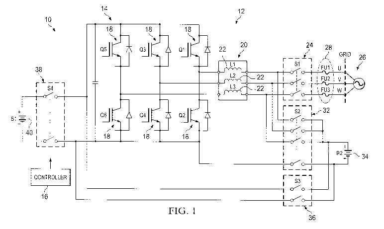
Turning now to the drawings, FIG. 1 illustrates an embodiment of a power
conversion
system 10 that includes a multi-mode energy router (MMER) 12. The MMER 12
includes a
functional block 14 of power electronics under processor control. The power
conversion
system 10 includes a controller 16 having a processor and a memory for
controlling the
power electronics of the MMER 12, among other things. It should be noted that
the term
"controller 16" in the present disclosure may refer to one or more controller
having a
processor and/or memory that are communicatively coupled to each other to
perform the
desired control tasks. The functional block 14 of power electronics may
include a triple half
bridge bi-directional converter/inverter functional power control building
block. Although
4
CA 02965488 2017-04-21
WO 2016/064872
PCT/US2015/056456
the illustrated embodiment features three half bridge units to provide 3 phase
power
conversion, other embodiments may utilize more or less than three half bridge
units
depending on the requirements of the application. Under processor control of
the controller
16, the functional block 14 may provide AC to DC (AC ¨ DC), DC to DC (DC ¨
DC), or DC
to AC (DC ¨ AC) power conversion functions or, in some cases, simultaneous
combinations
of these functions. Thus, the functional block 14 may function as a universal
power flow
(UPF) building block for electricity conversion.
In the illustrated embodiment, the functional block 14 may include a triple
half bridge
converter/inverter having six transistors 18 (e.g., IGBTs) used to convert
power between
different modes. The transistors (Q1-Q6) 18 are individually controlled by the
controller 16
to convert incoming power to a desired AC or DC power output. The MMER 12 also
may
include a block 20 of inductors 22 (L1 -L3) coupled to the functional block
14. As described
in detail below, the block 20 of inductors 22 may act as a storage element in
some power
conversion modes (e.g., DC - DC), or as a power conditioning filter in other
modes (e.g., AC
-DC).
The controller 16 may carefully control the individual transistors 18 so that
the main
functional block 14 can operate in a range of power conversion modes as
desired to convert
power between multiple different components. In some embodiments, the
controller 16 may
provide interleaved control of the transistors 18 to allow for this
individualized control. The
controller 16 may control the transistors 18 to selectively operate the
functional block 14 as a
power inverter that changes incoming DC power to AC power, to operate the
functional
block 14 as a rectifier that changes incoming AC power to DC power, or to
operate the
functional block 14 to act as a DC-DC converter (e.g., buck or boost
converter) that changes
incoming DC power from one voltage to another. In some embodiments, the
transistors 18
may be controlled to operate the functional block 14 in multiple modes at
once.
FIGS. 2-5 illustrate various switching schemes for the transistors 18 in the
functional
block 14, which may be implemented via the controller 16. Specifically, FIGS.
2-5 illustrate
different control schemes for operating the transistors 18 when the MMER 12 is
operated in
AC/DC mode, in DC/DC buck mode, in DC/DC boost mode, and in a three-phase
interleaved
DC/DC boost mode, respectively.
FIGS. 2A and 2B show the gate signals of six IGBTs (transistors 18 of FIG. 1)
when
the MMER is operated in AC/DC mode. In this AC/DC mode, MMER may be controlled
as
a traditional grid-tie inverter/rectifier. FIG. 2A includes a first plot 100
showing a carrier
5
CA 02965488 2017-04-21
WO 2016/064872
PCT/US2015/056456
signal 102 (10 kHz triangular waveform) and reference signal (sinusoidal
waveform) of U, V,
and W in three phases. These signals from U, V, and W may be signals
indicative of current
flowing from/to the grid. The illustrated CMPR1 104, CMPR2 106, and CMPR3 108
represent the reference signals of the phases U, V, and W, respectively.
FIGS. 2A and 2B also includes several plots 110, 112, 114, 116, 118, and 120
showing the gate signals of six different IGBTs that may form the functional
block 14 of FIG.
1. Specifically, the plot 110 illustrates a gate signal A P for the upper IGBT
labeled Q1
shown in FIG. 1. Similarly, the plot 112 illustrates a gate signal A_N for the
lower IGBT
labeled Q2. The plot 114 illustrates a gate signal B_P for the upper IGBT
labeled Q3, and the
plot 116 illustrates a gate signal B_N for the corresponding lower IGBT
labeled Q4.
Furthermore, the plot 118 illustrates a gate signal C P for the upper IGBT
labeled Q5, while
the plot 120 illustrates a gate signal C_N for the corresponding lower IGBT
labeled Q6.
The controller 16 of FIG. 1 may operate the functional block 14 of transistors
in an
AC/DC conversion mode according to the control logic provided below. In the
below
expression 1, the value Vtri represents the voltage value of the triangular
waveform carrier
signal 102 shown in the first plot 100 of FIG. 2A.
If Vtri > CMPR1, A_P = 1, AN = 0;
If Vtri < CMPR1, A_P = 0, A_N = 1;
If Vtri > CMPR2, B P = 1, B N = 0;
If Vtri < CMPR2, B_P = 0, B N = 1;
If Vtri > CMPR3, C P = 1, C_N = 0;
If Vtri < CMPR3, C_P = 0, C_N = 1.
(1)
FIGS. 3 and 4 show the gate signals of six IGBTs (transistors 18 of FIG. 1)
when the
MMER is operated in DC/DC mode. The MMER 12 can realize bi-directional power
flow
between source/loads B1 (e.g., 40 of FIG. 1) and B2 (e.g., 34 of FIG. 2), as
described in
detail below. When the MMER 12 operates as a buck converter, power may be
controlled to
flow from B1 to B2. In the DC/DC buck mode, lower IGBTs Q2, Q4, and Q6 of the
functional block 14 may be controlled "off' at all times, such that they are
used as
freewheeling diodes. When the MMER 12 operates as a boost converter, power may
be
controlled to flow from B2 to B1 . In the DC/DC boost mode, upper IGBTs Q 1 ,
Q3, and Q5
of the functional block 14 may be controlled "off' at all times, such that
they are used as
freewheeling diodes. In both the buck and boost DC/DC conversion modes, the
three
6
CA 02965488 2017-04-21
WO 2016/064872
PCT/US2015/056456
branches of the functional block 14 may be controlled independently as three
buck or boost
converters.
FIGS. 3A-3C show the gate signals of six IGBTs when the MMER is operated in a
DC/DC buck mode. FIGS. 3A-3C include three series 130, 132, and 134 of plots
representing the control scheme used in each of the three branches of the
functional block 14
when operating in this mode. Each of these series 130, 132, and 134 of plots
includes a plot
136 illustrating both a duty cycle 138 (Da, Db, and Dc) of the corresponding
branch (or arm)
along with the carrier signal 102 (10 kHz triangular waveform). The series
130, 132, and 134
each also include a plot 140 illustrating a gate signal (e.g., A_N, B_N, C_N)
of the lower
IGBTs Q2, Q4, and Q6 of FIG. 1. In addition, the series 130, 132, and 134 each
include a
plot 142 illustrating a gate signal (e.g., A_P, B_P, C_P) of the upper IGBTs
Ql, Q3, and Q5.
As illustrated, the controller may operate the functional block of transistors
in a
DC/DC buck conversion mode according to the control logic provided below. In
the below
expression 2, the value Vtri represents the voltage value of the triangular
waveform carrier
signal 102 shown in the first plots 136a, 136b, and 136c of the series 130,
132, and 134 of
FIGS. 3A-3C.
If Vtri_converter_a > Da, A_P = 0, AN = 0;
If Vtri_converter_a < Da, A_P = 1, A_N = 0;
If Vtri_converter_b > Db, B_P = 0, B_N = 0;
If Vtri_converter_b < Db, B_P = 1, B_N = 0;
If Vtri_converter_c > Dc, C_P = 0, C_N = 0;
If Vtri_converter_c < Dc, C P = 1, C_N = 0.
(2)
FIGS. 4A-4C show the gate signals of six IGBTs when the MMER is operated in a
DC/DC boost mode. FIGS. 4A-4C include three series 150, 152, and 154 of plots
representing the control scheme used in each of the three branches of the
functional block 14
when operating in this mode. Each of these series 150, 152, and 154 of plots
includes a plot
156 illustrating both the duty cycle 158 (Da, Db, and Dc) of the corresponding
branch (or
arm) along with the carrier signal 102 (10 kHz triangular waveform). The
series 150, 152,
and 154 each also include a plot 160 illustrating a gate signal (e.g., AN,
B_N, C_N) of the
lower IGBTs Q2, Q4, and Q6 of FIG. 1. In addition, the series 150, 152, and
154 each
include a plot 162 illustrating a gate signal (e.g., A_P, B_P, C P) of the
upper IGBTs Ql, Q3,
and Q5.
7
CA 02965488 2017-04-21
WO 2016/064872
PCT/US2015/056456
As illustrated, the controller may operate the functional block of transistors
in a
DC/DC boost conversion mode according to the control logic provided below. In
the below
expression 3, the value Vtri represents the voltage value of the triangular
waveform carrier
signal 102 shown in the first plots 156a, 156b, and 156c of the series 150,
152, and 154 of
FIGS. 4A-4C.
If Vtri converter_a > Da, A_P = 0, A N = 0;
If Vtri converter _a < Da, A_P = 0, A_N = 1;
If Vtri_converter b > Db, B_P = 0, B_N = 0;
If Vtri_converter b < Db, B_P = 0, B_N = 1;
If Vtri converter_c > Dc, C_P = 0, C_N = 0;
If Vtri converter c < Dc C _P=0 C N= 1.
(3)
Since the three arms of the function block 14 of FIG. 1 can be controlled
independently, the MMER may be controlled as a three-phase interleaved DC/DC
converter
to reduce input and output current ripple. FIGS. 5A and 5B show the input and
output
current of the MMER 12 when it is operated in a boost converter mode, although
it could be
similarly controlled to operate in a buck converter mode. FIGS. 5A and 5B
include several
plots 170, 172, 174, 176, 178, 180, and 182 to illustrate the interleaved
control. The first
three plots 170, 172, and 174 illustrate the duty cycle 158 (Da, Db, and Dc)
of the
corresponding branch (or arm) along with the carrier signal 102 (10 kHz
triangular
waveform). The fourth plot 176 illustrates input currents 184 (Ia dc in,
Ib_dc_in, and
Ic_dc_in) for each of the three branches, and these input currents 184 are
also the inductor
current of the three branches. Similarly, the sixth plot 180 illustrates
output currents 186
(Ia dc out, Ib_dc_out, and Ic dc_out) for each of the three branches, and
these output
currents 186 are also the diode current of the three branches.
As illustrated, the carrier signals 102 of the three arms have a 120 degrees
phase shift
(1/3 period) with respect to each other. Therefore, the input current ripple
(plot 176) and
output current ripple (plot 180) of each of the three arms also have a 120
degree phase shift
with respect to each of the other arms. The fifth plot 178 illustrates the
total input current
188, which is a sum of the input currents 184 in the three arms. The seventh
plot 182
illustrates the total output current 190, which is a sum of the output
currents 186 in the three
arms. As illustrated, the total input current 188 and the total output current
190 have a
smaller current ripple than would be available using a non-interleaved
converter.
8
CA 02965488 2017-04-21
WO 2016/064872
PCT/US2015/056456
Turning back to FIG. 1, the disclosed MMER 12 may include one or more of the
functional blocks 14 (UPFs) and a switch matrix (e.g., S1-S4) whereby power
from specific
sources or loads may be routed to the input or output of the functional block
14 under
processor control. That is, the MMER 12 includes a switch matrix
communicatively coupled
to the controller 16 and used to switch the coupling of the functional block
14 between
different sources and/or loads. The switch matrix may include several sets
of
electromechanical and/or semiconductor switches used to selectively couple the
desired
sources and loads to the functional block 14.
In the illustrated embodiment, for example, the switch matrix may include an
AC
switch 24 (Si) used to selectively couple an AC power source/load such as a
power grid 26
(coupled to fuses 28) to a three phase side of the functional block 14.
Another switch 32 (S2)
may be controlled to selectively couple a DC power source/load 34 to the three
phase side of
the functional block 14. In addition, a DC switch 36 (S3) may be controlled to
selectively
couple the DC power source/load 34 to the DC side of the functional block 14.
Furthermore,
a DC switch 38 (S4) may be controlled to selectively couple another DC power
source/load
40 to the DC side of the functional block 14.
In the illustrated configuration, the controller 16 may control the switches
24, 32, 36,
and 38 to move them into open or closed positions, in order to facilitate a
desired power
conversion between the various sources/loads. More specifically, the
controller 16 may
control the switches 24, 32, 36, and 38 according to the control scheme
outlined in Table 1 to
connect the desired source/load components of the power conversion system 10
to the
MMER 12. For example, when bi-directional power flow is desired between the
grid 26 and
B1 source/load 40, the controller 16 may close the Si and S4 switches 24 and
38 and open
the S2 and S3 switches 32 and 36. When bi-directional power flow is desired
between the
grid 26 and B2 source/load 34, the controller 16 may close the Si and S3
switches 24 and 36
and open the S2 and S4 switches 32 and 38. When bi-directional power flow is
desired
between the B1 source/load 40 and the B2 source/load 34, the controller 16 may
close the S2
and S4 switches 32 and 38 and open the Si and S3 switches 24 and 36.
Allow bidirectional power flow
Grid < S4> B1 Si &S4 closed, S2 &S3 open
between Grid and B1
Allow bidirectional power flow
S
Grid <l, S3> B2 Si &S3 closed, S2 &S4 open
between Grid and B2
9
CA 02965488 2017-04-21
WO 2016/064872 PCT/US2015/056456
Allow bidirectional power flow
.52, S4
B1 < > B2 S2 &S4 closed, Si &S3 open
between B1 and B2
Table 1: Switch matrix control scheme
The inductors 22 may perform different functions depending on the type of
power
conversion being performed by the MMER 12. When the functional block 14 is
operating as
an AC-DC power converter (e.g., inverter or rectifier), the inductors 22 may
function as
power conditioning AC-DC filters. When the functional block 14 is operating as
a DC-DC
power converter (e.g., buck or boost converter), the inductors 22 may function
as energy
storage elements. The inductors 22 may be selected so that they have an
inductance within
acceptable ranges for both the desired AC-DC and DC-DC power conversion modes,
or
different inductors may be switched into the circuit for AC-DC and DC-DC power
conversion modes.
The controller 16 may control the transistors 18 of the functional block 14
and the
switching matrix together to perform the desired power conversion between any
number of
loads and sources coupled to the MMER 12. For example, when it is desired to
convert DC
power from one of the DC power source/loads (e.g., B1 or B2) to the power grid
26, the
controller 16 may close and open the appropriate switches to electrically
couple the
functional block 14 between the desired source/load and the grid 26.
Simultaneously, or
nearly simultaneously, the controller 16 may provide signals to operate the
transistors 18 such
that the DC power signal from the source is converted to AC power signals that
are
synchronized and displaced 120 degrees from each other. From here, the AC
power signals
are filtered and sent to the grid 26. An opposite process may be used to
control the transistors
18 to convert three-phase AC power from the grid 26 to DC power provided to
the
appropriate source/load.
At other times, it may be desirable to convert DC power from one of the DC
power
source/loads to another DC power source/load. For example, in the illustrated
embodiment,
the B1 source/load 40 may represent a battery in an electric vehicle and the
B2 source/load 34
may represent a stationary battery associated with the MMER 12. These
source/loads 40 and
34 may operate at different voltages. The controller 16 may close and open the
appropriate
switches (e.g., Si and S3 open, S2 and S4 closed) to electrically couple the
functional block
14 between the two source/loads 40 and 34. Simultaneously, or nearly
simultaneously, the
controller 16 may provide signals to operate the transistors 18 at an
interleaved carrier
frequency to provide power from one DC source/load to the other.
CA 02965488 2017-04-21
WO 2016/064872
PCT/US2015/056456
The inductors 22 may function to provide an appropriate decrease or increase
in
voltage between the DC source/loads 40 and 34 to account for the difference in
operating
voltages of these components. When the controller 16 controls the transistors
18 to move the
electrical current from the B1 source 40 (e.g., vehicle) to the B2 load 34
(e.g., stationary), the
functional block 14 operates as a buck converter, since the inductors 22
effectively step the
voltage down from a higher voltage to a lower voltage. When the controller 16
controls the
transistors 18 to move the electrical current from the B2 source 34 (e.g.,
stationary) to the B1
load 40 (e.g., vehicle), the functional block 14 operates as a boost
converter, since the
inductors 22 effectively step the voltage up from the lower voltage to the
higher voltage.
In the manner described above, the MMER 12 may include a single functional
block
14 of power electronics that provides power conversion across a variety of bi-
directional
loads and sources that operate in the same or different modes. Traditionally,
multi-mode
power conversions between AC and DC sources/loads involve the use of two power
conversion stages (one AC-DC conversion and then one DC-DC conversion).
However, the
presently disclosed power conversion system 10 may utilize a single converter
(functional
block 14) that is precisely controlled to facilitate power conversion between
AC power (e.g.,
grid 26) and DC power (source/load 34 or source/load 40). In this way, the
MMER 12
provides a more efficient method of converting power between sources and loads
that operate
in different modes.
Furthermore, the system architecture of the disclosed MMER 12 is highly
flexible,
being able to accommodate AC or DC sources or loads. The power conversion
system 10
may be scalable, so that any desirable number, type, or operating mode of
additional
source/loads can be combined with the MMER 12. That is, instead of one
connection to grid
26 and two connections to DC power source/loads, the illustrated MMER 12 may
include
switching components for selectively coupling a greater number of sources and
loads to the
functional block 14 used to provide the desired power conversion. These
components may be
relatively easy to accommodate by adding new switches and programming the
controller 16
to control the switches and transistors as desired. The disclosed power
conversion system 10
may enable implementation of complex power systems using relatively little
hardware. This
makes the system 10 lower cost compared to existing power conversion systems.
In addition,
as noted above, the MMER 12 may utilize a single conversion process to improve
the power
efficiency of the multi-mode conversion process.
In the illustrated MMER 12 of FIG. 1, all the inductors 22 are arranged
11
CA 02965488 2017-04-21
WO 2016/064872
PCT/US2015/056456
asymmetrically (to the right side) with respect to the switching devices (main
functional
block 14). In some applications, this placement of the inductors 22 may be
restricting. For
example, when this inductor placement is used for DC/DC operations (buck or
boost
conversion), DC power that flows from right to left through the main
functional block 14 and
the inductors 22 (Fig 1 of the Application Draft) will be boosted, while DC
power that flows
from left to right through this system will be reduced (buck conversion). The
practical
impact of this restriction is that the voltage of the source/load (e.g., B1)
connected to the left
side of the main functional block 14 and the inductors 22, in the specific
conversion, must be
greater than the voltage of the other source/load conversion (e.g., B2)
connected to the right
side of the main functional block 14 and inductors 22.
For some applications, this constraint of having a "higher voltage to left
side" and a
"lower voltage to right side" may not be a challenging restriction. For
example, if the
source/load 40 to the left is a vehicle battery and the source/load 34 to the
right is a stationary
battery, there may be sufficient freedom in specifying the voltages of the
various batteries
and grid connections at play within the system 10. Even where source/load
voltages are more
constrained, additional contactors may be added to switch the source/loads
between the right
and left sides of the functional block 14, depending on the voltage of the
other source/load
involved in specific conversions. An example of this is the contactor S3
(e.g., 36) in FIG. 1,
which facilitates a connection between the B2 source/load 34 and the left
(higher voltage)
side of the main functional block 14. Thus, closing the S3 contactor 36 may
connect the B2
source/load 34 to the higher voltage (left) side so that grid voltage is
boosted up for charging
the B2 load 34. With the S3 contactor 36 open and the S2 contactor 32 closed,
the B2
source/load 34 may be connected to the lower voltage (right) side of the main
functional
block 14 so that its voltage can be boosted up to a higher B1 voltage for
charging the B1 load
40 from the B2 source 34.
In other embodiments of the power conversion system 10, however, this voltage
dependency of conversion may be undesirable, especially with source/loads that
have wide
variation in voltage. Photovoltaic systems are an example of such a source
that may have a
wider variation in voltage, although other source/loads could also have this
performance.
With a source/load having voltage that varies over a wide range, power
conversion may have
to be stopped so the source/load can be switched to the other side of the MMER
12. Such a
discontinuity in power flow may be undesirable.
Certain embodiments of the MMER 12 may be designed with the energy storage
12
CA 02965488 2017-04-21
WO 2016/064872
PCT/US2015/056456
inductors used for DC conversions connected symmetrically in the middle of two
branches of
the main functional block 14. This may be accomplished through different
placement of
contacts and switches within the MMER 12. FIG. 6 illustrates one example of an
embodiment of the MMER 12 having the symmetric (for DC conversions) placement
of the
inductors 22.
As illustrated, the MMER 12 may include similar features as the MMER 12 shown
in
FIG. 1, but may feature a differently arranged switching matrix. For example,
the illustrated
MMER 12 may include a switch 50 (S3) that may be controlled to selectively
couple the DC
power source/load 34 to the three phase side of the functional block 14 using
only two
contacts. In addition, the DC switch 36 (S3 old) may be controlled to
selectively couple the
DC power source/load 34 to the DC side of the functional block 14. The DC
switch 38 (S4)
may be controlled to selectively couple the DC power source/load 40 to the DC
side of the
functional block 14. Further, the MMER 12 may include a switch/contact 52 (S2)
disposed
along a line between a first branch 54a of the functional block 14 and a third
branch 54c of
the functional block 14 to the right of the inductors 22. Still further, the
MMER 12 may
include another switch/contact 56 (S5) disposed between the second and third
branches 54b
and 54c of the functional block 14.
With the S2 switch 52 closed, an energy storage inductor for the DC/DC
conversions
may be implemented with two of the three inductor coils 22 of the three-phase
inductor block
20. Since current is essentially complementary in the two coils, the three-
phase inductor
block 20 may have to be wound as three separate inductors 22 rather than as a
three-phase
inductor wound on a common core. The energy storage (DC) inductors 22 may thus
be
connected symmetrically between two of the three half bridge branches (e.g.,
54a and 54c) of
main functional block 14. The result of this symmetric converter is that wide
range DC
conversions may be accomplished in an essentially continuous manner. That is,
the MMER
12 may be capable of transitioning from buck DC conversion to boost DC
conversion using
modulation control of the functional block 14 rather than by changing switches
(S 1-S5). This
may enable power to flow either from higher to lower voltage (buck) or from
lower to higher
voltage (boost), no matter which side the higher or lower voltage source/load
may be relative
to the main functional block 14 at any time.
The S5 switch 56 may allow the third branch (54c) half-bridge of the main
functional
block 14 to form a separate connection to the functional block 14. That is,
with the S5 switch
56 open and the S2, S3, and S4 switches 52, 50, and 38 closed, power from/to
the B1 DC
13
CA 02965488 2017-04-21
WO 2016/064872
PCT/US2015/056456
source/load 40 can enter/leave the main functional block 14 on the collector
side of the upper
switching device in the left most half-bridge branch 54a. In addition, power
from/to the B2
source/load 34 can enter/leave the main functional block 14 at the collector
side of the upper
switching device in the right most half-bridge branch 54c.
Although in the illustrated
embodiment the far left and far right half-bridge branches 54a and 54c are
used, any pair of
the half-bridge branches (54, 54b, 54c) can be used. Also, as noted above,
although the
switches are illustrated as mechanical switches, they could be solid-state
transistor based
switches or other connection devices.
FIG. 7 illustrates another embodiment of the MMER 12 having a symmetric energy
storage inductor for DC/DC conversions. This embodiment is similar to the MMER
12 of
FIG. 6, but instead features a separate inductor 70 (L4) for DC conversions,
in addition to the
inductor block 20 used to filter signals during AC conversions. This
arrangement may be
particularly desirable since it can be difficult to have a three-phase
inductor that is capable of
providing filtering for AC and without any DC bias also handling the energy
storage and the
DC bias used for DC conversion. FIG. 7 shows the separate DC inductor 70
(choke)
connected between the symmetric first branch half-bridge 54a and the third
branch half-
bridge 54c. This connection may be implemented via a contact 72 (S2) on the
left side of the
inductor block 20. The contactor 36 (labeled S3_old in FIG. 6) and the
additional path
associated with it are not present in the illustrated embodiment. Thus, the
symmetric DC
conversion embodiment of FIG. 7 may include a version of the MMER 12 with a
relatively
simple circuit design.
While the MMER 12 illustrated in FIG. 7 is symmetric for DC/DC conversions, it
is
generally asymmetric for AC/DC conversions. Generally, this asymmetric design
is not a
restriction. However, the power transfer capabilities for the DC/DC conversion
using the
MMER 12 of FIG. 7 may be less than the power transfer capabilities for AC/DC
conversions,
since the illustrated MMER 12 uses only a single half-bridge branch to supply
DC conversion
power.
In some embodiments, it may be desirable to provide a power conversion system
10
that features a circuit that is fully symmetric for both DC/DC conversions and
three-phase
AC power transfers. FIG. 8 illustrates one example of such a power conversion
system 10.
The illustrated system effectively functions like two MMERs 12 coupled back-to-
back
(serially). In this embodiment, no additional DC inductors (chokes) are used.
In FIG. 8, the
MMERS 12a and 12b may include functional blocks 14a and 14b and inductor
blocks 20a
14
CA 02965488 2017-04-21
WO 2016/064872
PCT/US2015/056456
and 20b, respectively.
In the illustrated embodiment, the Si switch 24 may be controlled to
selectively
couple the grid 26 (and corresponding fuses 28) to the three-phase side of the
upper
functional block 14a. In addition, the system 10 may include a switch 90 (S2)
that may be
controlled to selectively couple the grid 26 (and corresponding fuses 28) to
the three-phase
side of the lower functional block 14b. The system 10 may also include the S4
switch 38 that
may be controlled to selectively couple the DC power source/load 40 to the DC
side of the
upper functional block 14a. Further, the system 10 may include a switch 92
(S3) that may be
controlled to selectively couple the DC power source/load 34 to the DC side of
the lower
functional block 14b.
In this embodiment, the power transfer enabled by the two back-to-back
functional
blocks 14 (three-phase inverters), connected through the S2 switch 90, is AC
power transfer.
This AC power transfer may be used even for DC/DC conversions between the DC
source/loads 34 and 40. Each main functional block 14 and inductor group 20
may be
operating in three-phase synthesis (inversion) mode. Thus, the relative phase
between the
two inverters 14 may determine power flow. For example, whichever functional
block 14 is
operating with the leading phase angle delivers power, while the functional
block with the
lagging phase angle receives power. In embodiments where DC power is provided
to the
receiving load, this power flow may be cycle discontinuous, and so may be
filtered, although
this is not shown in FIG. 8. The illustrated system 10 may be used to transfer
power from the
B1 load/source 40 to the B2 load/source, or vice versa, regardless of which of
these
load/sources has the greater voltage, within the range allowed by the
inductors 20a and 20b.
Power can be transferred from either DC source/load (e.g., 34 or 40) to the
grid 26 by
inversion mode or from the grid 26 to either or both of the DC source/loads 34
and 40 by
active rectification mode. The grid 26 and either of the DC source/loads
(e.g., 34, 40) may
jointly deliver power to the other DC source/load (e.g., 40, 34). And, as
noted above,
additional DC source/loads may be connected to the DC side of either
functional block 14 as
is done with the S3 switch 92 or S4 switch 38. Also, additional AC
source/loads (e.g., grid
26) can be added with contactors similar to the Si switch 24.
FIG. 9 illustrates an embodiment of a power conversion system 10 that may
utilize the
MMER 12 to connect multiple different sources or loads. In the illustrated
embodiment, for
example, the MMER 12 is coupled to a photovoltaic (PV) cell power source 210,
the power
grid 26, another source or load 212, an electric bus 214, a stationary battery
216, and another
CA 02965488 2017-04-21
WO 2016/064872
PCT/US2015/056456
power generation source 218. Some of these components (e.g., PV cell power
source 210
and power generation source 218) may be configured to only act as a power
source, while
other components (e.g., electric bus 214) may function only as a load
requiring power. Still
other components (e.g., grid 26, source or load 212, and battery 216) may be
operable as
either a power source or a load, depending on the power needs at the time.
These
components may operate in different electrical modes, such as three phase AC
power for the
grid 26 and DC power for the battery 216.
As described above, the MMER 12 may include a single power conversion
functional
block designed to perform the desired power conversion between any two of the
attached
components. Thus, the MMER 12 provides a bi-directional and multi-mode power
connection between the multiple components coupled thereto. The components may
be
attached to the functional block via the switching matrix described above in
relation to any of
FIGS. 1, 6, 7, or 8. The controller 16 may control the switching matrix and
the functional
block of the MMER 12 to selectively couple the desired components to the
functional block
and to facilitate the desired power conversion between the components.
The controller 16 may change the power conversion process being performed
throughout the lifetime of the MMER 12. For example, the MMER 12 may convert
energy
from the grid 26 to the electric bus 214, and then change to converting energy
from the PV
cell source 210 to the grid 26. The power conversion being performed by the
MMER 12 may
be controlled based on user preference. In some embodiments, the controller 16
may change
the power conversion being performed by the MMER 12 based on timing (e.g.,
using the PV
cells 210 to power the electric bus 214 during the day and using the battery
216 to power the
electric bus 214 at night). In other embodiments, the controller 16 may change
the power
conversion operation based on availability of electrical power from the
various sources (e.g.,
converting energy from the grid 26 to recharge a battery 216 that has run
low). In still other
embodiments, the controller 16 may change the power conversion process based
on a user
prescribed order of source components to be depleted or load components to be
powered.
The single MMER 12 described above with reference to FIGS. 1, 6, 7, or 8 can
be
used as a building block of larger power conversion systems, especially where
mixed-mode
conversions are performed using several source/loads. An example of this, as
described with
reference to the electric bus application of FIG. 9, may involve supplying
power from the
grid 26 simultaneously with power from photovoltaic panels 210 or power from a
stationary
battery 216 and delivering this power to the battery of the electric bus 214.
Other variations
16
CA 02965488 2017-04-21
WO 2016/064872
PCT/US2015/056456
and combinations of source/loads may be utilized in other embodiments. Such
complex
power flow situations could easily occur in practice.
As discussed at length above, the basic MMER 12 may allow power flow from a
single source to a single load at any one time and, thus, may not be able to
fully handle
multiple power sources contributing power in a conversion or multiple loads
receiving power
in a conversion. To address these more complex situations, additional branches
(pairs of
switching transistors 18 of FIG. 1) in the main functional block 14 and more
switches or
contactors could be added to the power conversion system 10. However, instead
of using a
more complex MMER, other systems 10 may be designed that utilize the basic
MMER 12 as
a building block that is reproduced in its general form as a convenient way to
build complex
power conversion systems.
Two or more MMERs 12 may be controlled to facilitate full power conversion
between three different power source/loads. The controller 16 may carefully
control the
individual transistors 18 so that each MMER 12 can convert power from multiple
sources to a
single load, or convert power from the same source to multiple loads. Examples
of this
would include power conversions from both the grid 26 and the B2 source 34
delivered to the
B1 load 40, or power conversions from the grid 26 to both the B1 load 40 and
the B2 load 34.
FIGS. 10A and 10B illustrate an example of a power conversion system 10 using
two
MMERs 12a and 12b. In certain embodiments, the power conversion system 10 may
be an
electric vehicle charging station, as described above with reference to FIG.
9. The B1
source/load 40 may include a battery that is connected to both of the MMERs 12
and is
considered to be in an electric bus or other vehicle. As such, the B1
source/load 40 may be
mobile so that it can be selectively connected to or disconnected from the
MMER system.
The B2 source/load may include a stationary battery that is always connected
to both of the
two MMERs 12. The mobile and stationary aspects of these source/loads 34 and
40 are for
example only and are not requirements for a multiple MMER system as
illustrated in FIGS.
10A and 10B. Other sources of power and/or loads can be included as well in
the system 10,
and the system 10 can include more than two MMERs 12.
The illustrated two MMER system is connected to a three-phase AC power
source/load (e.g., grid 26). The system of MMERs 12 may be designed to
maintain the time
averaged power taken from the grid 26 as nearly constant as possible while the
power
provided to the vehicle battery (B1 source/load 40) varies greatly. This may
be a particularly
desirable constraint for large power sources or loads that are connected to
the electricity grid
17
CA 02965488 2017-04-21
WO 2016/064872
PCT/US2015/056456
26, as it may aid in the stability of the grid 26.
Having generally described the layout of the two MMER power conversion system
10, a more detailed description of the operation of the system 10 will be
provided. Such
operation of the system 10 may begin when the B1 source/load 40 is connected
to the
MMERs 12 and is being charged. One MMER (e.g., the upper MMER 12a) may include
connections made to the B1 source/load 40 and the B2 source/load 34 (S2 and S4
switches
32a and 38a closed), and the MMER 12a may operate under the control mode as a
DC/DC
boost converter, as controlled by controller 16a. Power may flow from the B2
source 34 and
be delivered to the B1 load 40. The other MMER (e.g., the lower MMER 12b) may
include
connections made to the grid 26 and to the B1 source/load (zS1 and zS4
switches 24b and
38b closed), and the MMER 12b may operate under the control mode as a three
phase
rectifier taking power from the grid 26 and delivering the power to the B1
load 40. The grid
power level delivered by the lower MMER 12b may be controlled independently
(via
controller 16b) from the power coming from the B2 source 34 to the B1 load 40
through the
upper MMER 12a. The sum of the power levels supplied to the B1 load 40 may
charge the
battery Bl. This is shown in FIGS. 11A and 11B during the 1.0 to 1.5 time
interval.
The level of power into the B1 load 40 may decrease as the B1 battery becomes
charged. Although not shown in the waveforms of FIGS. 11A and 11B, the
decrease in
battery B1 power may initially be provided by a decrease in power from the B2
source 34
converted via the upper MMER 12a. This decrease may be relied on until the
power
provided to the B1 load 40 equals the grid power converted through the lower
MMER 12b.
At this point, the power out of the B2 source/load 34 through the upper MMER
12a may be
zero while the B1 battery charging power is fully provided by the grid 26
through the lower
MMER 12b.
The illustrated system 10 may be controlled to further reduce the B1 battery
charging
power without reducing grid power from the grid 26. This may be accomplished
in several
different ways. For example, the controller 16a may control the switches of
the upper
MMER 12a to connect the upper MMER 12 to the grid 26 and to the B2 source load
34 (open
S2 and S4, then close 51 and S3) and operate under the control mode as a three-
phase
rectifier, similar to the lower MMER 12b. The upper MMER 12a may then deliver
power
from the grid 26 to the B2 load 34. The amount of power supplied to the B2
load 34 by the
upper MMER 12a may increase directly as the power supplied to the B1 load 40
by the lower
MMER 12b is further reduced. The sum of the powers of the two MMERs 12a and
12b, both
18
CA 02965488 2017-04-21
WO 2016/064872
PCT/US2015/056456
supplied from the grid 26, may be controlled to equal the desired constant
power from the
grid 26.
Once the B1 load 40 is disconnected from the two MMER system, each of the
MMERs 12a and 12b may be adjusted to delivered equal parts (half) the power
supplied from
the grid 26 to the B2 load 34. This may result in equal heating within the
MMERs 12a and
12b. This final operating condition of the system 10 is shown in FIGS. 11A and
11B as
waveforms during the 0.0 to 1.0 and 1.5 to 2.0 intervals.
FIGS. 11A and 11B illustrate several plots 250, 252, 254, 256, 258, 260, 262,
and 264
showing waveforms that represent two of the control modes explained above with
reference
to the two MMER power conversion system 10 of FIG.10. These control modes may
include
the "start" mode from the 1.0 to 1.5 time interval and the "finish" mode from
the 0-1.0 and
1.5-2.0 time intervals. It should be noted that there are discontinuities
illustrated near the
times 1.0 and 1.5 in the waveforms of FIGS. 11A and 11B, but these are merely
a result of
simplifications in the simulation model and do not necessarily reflect actual
system
performance.
There are eight waveforms shown in FIGS. 11A and 11B. The first waveform 250
may represent the current of the B1 source/load 40. Positive current flows
into the B1
source/load 40 (charging), and negative current flows out of the B1
source/load 40
(discharging). The second waveform 252 may represent the current of the B2
source/load 34.
Similar to the first waveform 250, positive current flows into the B2
source/load 34
(charging) while negative current flows out of the B2 source/load 34
(discharging). The third
waveform 254 may represent the Root Mean Square (RMS) grid current. The fourth
waveform 256 may represent the instantaneous three phase grid current
available from the
grid 26.
The fifth waveform 258 may represent an instantaneous current through the
upper
MMER 12a. It should be noted that, during the 1.0 to 1.5 interval, the current
through the
upper MMER 12a is DC and therefore is equal in the three branches of the main
functional
block 14a of the MMER 12a. Thus, the total current contributed by the upper
MMER 12a to
the B1 source/load 40 may be three times the current shown in the plot 258.
The sixth
waveform 260 may represent a current control reference (and current feedback)
for the upper
MMER 12a. The seventh waveform 262 may represent the 3-phase instantaneous
current
through the lower MMER 12b. The eighth waveform 264 may represent a current
control
reference (and current feedback) for the lower MMER 12b.
19
CA 02965488 2017-04-21
WO 2016/064872
PCT/US2015/056456
In the simulation illustrated in FIGS. 11A and 11B, from 0 second to 1 second
both of
the MMERs 12a and 12b are generally operated as rectifiers converting incoming
AC power
from the grid 26 to charge the B2 source/load 34. During this period of time,
the current
control references for each MMER 12 may be the same (e.g., 0.45) and at half
of the level
(0.90) of the current control of the lower MMER 12b during the interval of 1.0
to 1.5
seconds. They may be equal so that power dissipation (i.e. heating) in the two
MMERs 12a
and 12b are equal and at the half level so the AC grid current RMS value
remains constant.
The current feedback of both the MMERs 12a and 12b may follow the respective
current
control reference, as shown.
In the illustrated simulation, from 1 second to 1.5 second the upper MMER 12a
generally operates as a boost converter, charging the B1 source/load 40 with
power from the
B2 source/load 34. During this period of time, the AC current control
reference of the upper
MMER 12a may be disabled (set to 0) because the upper MMER 12a is operated in
a DC/DC
boost converter mode. During this interval, the lower MMER 12b may continue to
operate as
a rectifier, taking power from the grid 26 and providing it to the B1
source/load 40 instead of
the B2 source/load 34. The current control reference for the lower MMER 12b
may go to the
AC grid RMS current level (e.g., 0.90) since it is the only MMER 12 taking
power from the
grid 26 during this time.
When operating the power conversion system 10 of FIGS. 10A and 10B, the power
of
the grid 26 may be carefully controlled so that the power conversion system 10
can adapt to
various scenarios. FIG. 12 illustrates a certain scenario in which the grid
power conversion
may be controlled. In the illustrated plot 270, a square waveform 272 may
represent the
charging power of the B1 source/load 40 (e.g., mobile battery) and a
horizontal straight line
274 may represent the power supplied by the grid 26. If the power conversion
system 10
(e.g., charging station) only relies on grid power to charge the B1
source/load 40, and the B2
source/load (e.g., stationary battery) is not used, the grid power may be
exactly the same as
the B1 charging power. The grid power used in this instance may have a high
peak to
average ratio, which may impose a burden on the electricity generation.
Typically, industrial
electricity customers with this sort of load can be financially penalized by
the electric
company with "demand charges." In order to avoid these charges by maintaining
a more
constant level of grid supplied power, the stationary battery B2 source/load
34 may be added
to the system 10.
As illustrated from the time 0 to ti seconds, the stationary battery B2
source/load 34
CA 02965488 2017-04-21
WO 2016/064872
PCT/US2015/056456
and the power grid 26 may charge the mobile battery B1 source/load 40
together. The
amount of electric energy flowing from grid 26 to the B1 source/load 40 may
equal the area
of 'C' 276 in the plot 270, and the amount of electric energy provided by the
B2 source/load
34 to charge the B1 source/load 40 may equal the area of 'A' 278 in the plot
270. From ti to
t2 seconds, the mobile battery B1 source/load 40 may leave the charging
station, such that the
power grid 26 charges only the stationary battery B2 source/load 34. The
amount of electric
energy that flows from the grid 26 to the B2 source/load 34 at this point may
equal the area of
'B' 280.
To keep a balance of charge in stationary battery (B2), the area of 'A' 278
may be
controlled to approximately equal the area of 'B' 280. It should be noted that
these
approximately equal areas in the plot 270 may be controlled neglecting certain
battery losses
(e.g., storage inefficiency, self-discharge, and aging) of the source/loads.
If the area of 'A'
278 is smaller than the area of 'B' 280, the energy that the B2 source/load 34
received from
grid may be greater than the energy that the B2 source/load 34 provided to the
B1 source/load
40. That may result in an increase of the long term State of Charge (SOC) in
the B2
source/load 34. If the area of 'A' 278 is larger than the area of 'B' 280, the
energy that the
B2 source/load 34 received from the grid 26 may be less than the energy that
the B2
source/load 34 provided to the B1 source/load. This may result in a decrease
of the long tem'
SOC in the B2 source/load 34. The area of 'B' 280 may be calculated as the
product of
average grid power and the time duration (t2 ¨ 0). The time interval (t2 - ti)
may represent
the time when the vehicle (e.g., B1) is not being charged.
A control algorithm may be utilized to control the average grid power supplied
to
either source/load so that the area of 'B' 280 can be maintained equal to the
area of 'A' 278.
Using this control algorithm, the power conversion system 10 may adjust the
average grid
power used based on power provided to charge the B1 source/load 40 (e.g.,
buses) and the
time between charging of the Bl source/load 40. Also, because of battery
aging, the energy
storage capability of the B2 source/load 34 (e.g., stationary battery) may
decrease over time.
Thus, the control algorithm may be adapted for various battery conditions of
aging, self-
discharge, and internal losses.
Although the present disclosure and its advantages have been described in
detail, it
should be understood that various changes, substitutions and alterations can
be made herein
without departing from the spirit and scope of the disclosure as defined by
the following
claims.
21