Note: Descriptions are shown in the official language in which they were submitted.
LED TUBE LAMP
FIELD OF THE INVENTION
[0002] The present invention relates to the features of LED incendiaries. More
particularly,
this invention describes various new and useful improvements for LED tube
lamps.
BACKGROUND OF THE INVENTION
[0003] LED lighting technology is rapidly developing to replace traditional
incandescent
and fluorescent lightings. LED tube lamps are mercury-free in comparison with
fluorescent tube
lamps that need to be filled with inert gas and mercury. Thus, it is not
surprising that LED tube
lamps are becoming a highly desirable illumination option among different
available lighting
systems used in homes and workplaces, which used to be dominated by
traditional lighting options
such as compact fluorescent light bulbs (CFLs) and fluorescent tube lamps.
Benefits of LED tube
lamps include improved durability and longevity and far less energy
consumption; therefore, when
taking into account all factors, they would typically be considered as a cost
effective lighting option.
[0004] Typical LED tube lamps have a variety of LED elements and driving
circuits. The
LED elements include LED chip-packaging elements, light diffusion elements,
high efficient heat
dissipating elements, light reflective boards and light diffusing boards. Heat
generated by the LED
elements and the driving elements is considerable and mainly dominates the
illumination intensity
such that the heat dissipation needs to be properly disposed to avoid rapid
decrease of the
luminance and the lifetime of the LED lamps. Problems including power loss,
rapid light decay, and
1
Date Recue/Date Received 2020-11-23
CA 02966755 2017-05-04
WO 2016/086900 PCT/CN2015/096501
short lifetime due to poor heat dissipation are always the key factors in
consideration of improving
the performance of the LED illuminating system. It is therefore one of the
important issues to solve
the heat dissipation problem of the LED products.
[0005] Nowadays, most of the LED tube lamps use plastic tubes and metallic
elements to
dissipate heat from the LEDs. The metallic elements are usually exposed to the
outside of the
plastic tubes. This design improves heat dissipation but heightens the risk of
electric shocks. The
metallic elements may be disposed inside the plastic tubes, however the heat
still remains inside the
plastic tubes and deforms the plastic tubes. Defonnation of the plastic tubes
also occurs even when
the elements to dissipate heat from the LEDs are not metallic.
[0006] The metallic elements disposed to dissipate heat from the LEDs may be
made of
aluminum. However, aluminum is too soft to sufficiently support the plastic
tubes when the
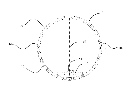
deformation of plastic tubes occurs due to the heat as far as the metallic
elements disposed inside
the plastic tubes are concerned.
[0007] As a result, the current related skills still could not be applied to
deal with the above-
mentioned worse heat conduction, poor heat dissipation, heat deformation, and
electric shock
defects. On the other hand, the LED tube lamp may be provided with power via
two ends of the
lamp and a user is easily to be electric shocked when one end of the lamp is
already inserted into an
terminal of a power supply while the other end is held by the user to reach
the other terminal of the
power supply. In view of these issues, the claimed invention and the preferred
embodiments are
proposed below.
OBJECTS AND SUMMARY OF THE INVENTION
[0008] Therefore, it is an object of the claimed invention to provide a
significantly
improved LED tube lamp that dissipates heat more efficiently. It is a further
object of the claimed
invention to provide an LED tube lamp that is structurally stronger. It is yet
another object of the
claimed invention to provide an LED tube lampthat minimizes the risk of
electric shocks.
[0009] In accordance with an exemplary embodiment of the claimed invention,
the LED
tube lamp comprises a lamp tube and an LED light assembly. The lamp tube
includes a light
transmissive portion, a reinforcing portion and an end cap. The LED light
assembly includes an
LED light source and an LED light strip. The reinforcing portion includes a
platform and a bracing
2
CA 02966755 2017-05-04
WO 2016/086900 PCT/CN2015/096501
structure. The bracing structure includes a horizontal rib and a vertical rib
and is fixedly connected
to the platform. The LED light assembly is disposed on an upper surface of the
platform. The upper
surface of the platform is coated with a reflective layer. The end cap is
attached to an end of the
lamp tube. The light transmissive portion and the reinforcing portion define a
dividing line between
them on a cross section of the lamp tube. Respective shapes of the light
transmissive portion and the
reinforcing portion, how the two portions interconnect to form the lamp tube
and, particularly, the
respective proportions of the two portions in the lamp tube depend on a
desired totality of
considerations such as field angle, heat dissipation efficiency and structural
strength. A wider field
angle __ potentially at the expense of heat dissipation capability and
structural strength is achieved
when the proportion of the light transmissive portion increases in relation to
that of the reinforcing
portion. By contrast, the lamp tube benefits from an increased proportion of
the reinforcing portion
in relation to that of the light transmissive portion in such ways as better
heat dissipation and
rigidity but potentially loses field angle.
[0010] In accordance with an exemplary embodiment of the claimed invention,
the aforesaid
LED light transmissive portion is made from light transmissive plastic. The
reinforcing portion is
made from thermally conducive plastic. The light transmissive plastic exhibits
a greater optical
transmittance but less thermal conductivity and structural strength than the
thermally conductive
plastic.
[0011] In accordance with an exemplary embodiment of the claimed invention, a
first cross
section of the end cap fully encloses a second cross section, defined on a
same plane that defines the
first cross section, of the reinforcing portion.
[0012] In accordance with an exemplary embodiment of the claimed invention,
the end cap
and the lamp tube are fastened together with a silicone-based adhesive having
a thermal
conductivity of at least 0.7 Wm-1K-1.
[0013] In accordance with an exemplary embodiment of the claimed invention,
the LED
tube lamp further comprises a layer of anti-reflection coating applied to an
inner surface of the lamp
tube. A thickness of the layer of anti-reflection coating is chosen to give
the coating an optical depth
of one quarter of the wavelength range coming from the LED light source. The
anti-reflection
coating has an upper boundary, which divides the inner surface of the lamp
tube and the anti-
reflection coating, and a lower boundary, which divides the anti-reflection
coating and the air in the
3
CA 02966755 2017-05-04
WO 2016/086900 PCT/CN2015/096501
lamp tube. Light waves reflected by the upper and lower boundaries of the
coating interfere with
one another to reduce reflectance.
[0014] In accordance with an exemplary embodiment of the claimed invention,
three
successive layers of anti-reflection coatings are applied to the inner surface
of the lamp tube to
obtain low reflectivity over a wide range of frequencies. The thicknesses of
the coatings are chosen
to give the coatings optical depths of, respectively, one half, one quarter
and one half of the
wavelength range coming from the LED light source. Tolerancefor the thickness
of the coating is
20%.
[0015] In accordance with an exemplary embodiment of the claimed invention,
the
thickness of the anti-reflection coating is chosen to give low reflectivity
over at least 60% of the
wavelength range beaming from the LED light source.
[0016] In accordance with an exemplary embodiment of the claimed invention,
the anti-
reflection coating is made from a material having a refractive index of a
square root of the index of
the lamp tube. Tolerance for the coating's refractive index is 20%.
[0017] In accordance with an exemplary embodiment of the claimed invention,
the lamp
tube includes a roughened inner surface. The roughened inner surface has a
greater roughness than
an outer surface of the lamp tube.
[0018] In accordance with an exemplary embodiment of the claimed invention,
the LED
light strip is made from flexible substrate material. The LED light strip
includes an electrically
conductive wiring layer. The LED light source is disposed on and electrically
connected to a first
surface of the wiring layer.
[0019] In accordance with an exemplary embodiment of the claimed invention,
the LED
light strip further includes a dielectric layer disposed on a second surface
of the wiring layer.
[0020] In accordance with an exemplary embodiment of the claimed invention,
the LED
light strip further includes a protection layer over the wiring layer and the
dielectric layer. The
protection layer is made from one of solder resists
[0021] In accordance with an exemplary embodiment of the claimed invention,the
lamp
tube further includes a ridge extending in an axial direction along an inner
surface of the lamp tube.
[0022] In accordance with an exemplary embodiment of the claimed invention,
the ridge is
an elongated hollow structure. The lamp tube further includes a maintaining
stick disposed inside
4
CA 02966755 2017-05-04
WO 2016/086900 PCT/CN2015/096501
the hollow structure of the ridge. The maintaining stick is made from a
material having a greater
stiffness than the material from which the lamp tube is made and the material
from which the LED
light strip is made.
[0023] In accordance with an exemplary embodiment of the claimed invention,
the
maintaining stick is made from a different material than the material from
which the reinforcing
portion is made.
[0024] In accordance with an exemplary embodiment of the claimed invention,
the LED
tube lamp comprises a lamp tube and an LED light assembly. The lamp
tubeincludes a light
transmissive portion, a reinforcing portion and an end cap. The LED light
assemblyincludes an
LED light source and an LED light strip. The reinforcing portion includes a
platform and a bracing
structure fixedly connected to the platform. The LED light assembly is
disposed on an upper
surface of the platform. The end cap is attached to an end of the lamp tube.
The light transmissive
portion and the reinforcing portion define a dividing line between them on a
cross section of the
lamp tube. The LED light strip includes a first metallic object. The bracing
structure includes a
second metallic object having a greater stiffness but less heatsinking
capability than the first
metallic object. The ratio of the volume of the first metallic object to the
volume of the second
metallic object in the lamp tube is from 0.001:1 to 100:1.
[0025] Various other objects, advantages and features of the present invention
willbecome
readily apparent from the ensuing detailed description, and the novel features
will be particularly
pointed out in the appended claims.
BRIEF DESCRIPTION OF FIGURES
[0026] The following detailed descriptions, given by way of example, and not
intended to
limit the present invention solely thereto, will be best be understood in
conjunction with the
accompanying figures:
[0027] Fig. us a cross-sectional view of the LED tube lamp with a light
transmissive
portion and a reinforcing portionin accordance with an exemplary embodiment of
the claimed
invention;
[0028] Fig. 2is a cross-sectional view of the LED tube lamp with a bracing
structurein
accordance with an exemplary embodiment of the claimed invention;
CA 02966755 2017-05-04
WO 2016/086900 PCT/CN2015/096501
[0029] Fig. 3 is aperspective viewof the LED tube lamp schematically
illustrating the
bracing structure shown in Fig.2;
[0030] Fig. 4 is a perspective viewof the LED tube lamp with a non-circular
end capin
accordance with an exemplary embodiment of the claimed invention;
[0031] Fig. 5 is across-sectional viewillustrating a vertical rib of the lamp
tubein accordance
with an exemplary embodiment of the claimed invention;
[0032] Fig. 6is across-sectional viewillustrating the bracing structure of the
lamp tube in
accordance with an exemplary embodiment of the claimed invention;
[0033] Fig. 7is across-sectional viewillustrating a ridge, which extends in an
axial direction
along an inner surface of the lamp tube, in accordance with an exemplary
embodiment of the
claimed invention;
[0034] Fig. 8 is across-sectional viewillustrating a compartment, which
isdefined by the
bracing structure of the lamp tube,in accordancewith an exemplary embodiment
of the claimed
invention;
[0035] Fig. 9is across-sectional viewillustrating the bracing structure of the
lamp tube in
accordance with an exemplary embodiment of the claimed invention;
[0036] Fig. 10 is aperspective viewof the lamp tubeshown in Fig.9;
[0037] Fig. 1 us across-sectional view illustrating the bracing structure of
the lamp tube in
accordance with an exemplary embodiment of the claimed invention;
[0038] Fig. 12 is across-sectional viewillustrating the LED light strip with a
wiring layer in
accordance with an exemplary embodiment of the claimed invention;
[0039] Fig. 13is aperspective viewof the lamp tube shown in Fig 12;
[0040] Fig. 14 is cross-sectional viewillustrating a protection layer disposed
on the wiring
layer in accordance with an exemplary embodiment of the claimed invention;
[0041] Fig. 15is aperspective viewof the lamp tube shown in Fig. 14;
[0042] Fig. l 6i s a perspective viewillustrating a dielectric layer disposed
on the wiring layer
adjacent to the lamp tube in accordance with an exemplary embodiment of the
claimed invention;
[0043] Fig. 17is aperspective viewof the lamp tube shown in Fig. 16;
6
CA 02966755 2017-05-04
WO 2016/086900 PCT/CN2015/096501
[0044] Fig. 18 is a perspective view illustrating a soldering pad on the
bendable circuit sheet
of the LED light strip to be joinedtogether with the printed circuit board of
the power supply in
accordance with an exemplary embodiment of the claimed invention;
[0045] Fig. 19 is a planar view illustrating an arrangement of the soldering
pads on the
bendable circuit sheet of the LED light strip in accordance with an exemplary
embodiment of the
claimed invention;
[0046] Fig. 20 is a planar view illustratingthree soldering pads in a row on
the bendable
circuit sheet of the LED light strip in accordance with an exemplary
embodiment of the claimed
invention;
[0047] Fig. 21 is a planar view illustratingsoldering pads sitting in two rows
on the bendable
circuit sheet of the LED light strip in accordancewith an exemplary embodiment
of the claimed
invention;
[0048] Fig. 22 is a planar view illustrating four soldering pads sitting in a
row on the
bendable circuit sheet of the LED light strip in accordance with an exemplary
embodiment of the
claimed invention;
[0049] Fig. 23 is a planar view illustratingsoldering pads sitting in a two by
two matrix on
the bendable circuit sheet of the LED light strip in accordancewith an
exemplary embodiment of the
claimed invention,
[0050] Fig. 24 is a planar view illustrating through holes formed on the
soldering pads in
accordancewithan exemplary embodiment of the claimed invention;
[0051] Fig. 25 is a cross-sectional view illustrating the soldering bonding
process, which
utilizes the soldering pads of the bendable circuit sheet of the LED light
strip shown in Fig. 30
taken from side view and the printed circuit board of the power supply,in
accordance with an
exemplary embodiment of the claimed invention;
[0052] Fig. 26 is across-sectional view illustrating thesoldering bonding
process,which
utilizes the soldering pads of the bendable circuit sheet of the LED light
strip shown in Fig. 24,
wherein the through hole of the soldering pads is near the edge of the
bendable circuit sheet,in
accordance with an exemplary embodiment of the claimed invention;
[0053] Fig. 27 is a planar view illustrating notches formed on the soldering
pads in
accordancewithan exemplary embodiment of the claimed invention;
7
CA 02966755 2017-05-04
WO 2016/086900 PCT/CN2015/096501
[0054] Fig. 28 is a cross-sectional view of the LED light strip shown in Fig.
27 along the
line A-A;
[0055] Figs. 29A-F areschematic viewsofan end cap including a safety switchin
accordance
with an exemplary embodiment of the claimed invention;
[0056] Fig. 30 is a schematic view of the end cap in accordancewith an
exemplary
embodiment of the claimed invention;
[0057] Fig. 31 is a perspective view of the circuit board assembly, which
comprisesthe
bendable circuit sheet of the LED light strip and the printed circuit board of
the power supply,in
accordance with an exemplary embodiment of the claimed invention;
[0058] Fig. 32 is a perspective view of an alternative arrangement of the
circuit board
assembly shown in Fig. 31; and
[0059] Fig. 33 is a perspective view of the printed circuit board of the power
supply,which
is perpendicularly adhered to a hard circuit board made of aluminum via
soldering,in accordance
with an exemplary embodiment of the claimed invention.
DETAILED DESCRIPTION OF THE EMBODIMENTS
[0060] Referring to Fig. 1, in accordance with an exemplary embodiment of the
claimed
invention, the LED tube lamp comprises a lamp tube 1 andan LED light assembly.
The lamp tube 1
includes a light transmissive portion 105 and a reinforcing portion 107. The
reinforcing portion 107
is fixedly connected to the light transmissive portion 105.
[0061] The LED light assembly is disposed inside the lamp tube 1 and includes
an LED
light source 202 and an LED light strip 2. The LED light source is thermally
and electrically
connected to the LED light strip 2, which is in turn thermally connected to
the reinforcing portion
107. Heat generated by the LED light source 202 is first transmitted to the
LED light strip 2 and
then to the reinforcing portion 107 before egressing the lamp tube 1. Thermal
connection is
achieved with thermally conductive tapes or conventional mechanical fasteners
such as screws
aided by thermal grease to eliminate air gaps from interface areas.
[0062] Typically, the lamp tube 1 has a shape of an elongated cylinder, which
is a straight
structure. However, the lamp tube 1 can takeanycurved structure such as a ring
or a horseshoe. The
cross section of the lamp tube 1 defines, typically, a circle, or not as
typically, an ellipse or a
8
CA 02966755 2017-05-04
WO 2016/086900 PCT/CN2015/096501
polygon. Alternatively, the cross section of the lamp tube ltakesanirregular
shape depending on the
shapes of, respectively, the light transmissive portion 105 and the
reinforcing portion 107 and on
the manner the two portions interconnect to form the lamp tube 1.
[0063] The lamp tube 1 is a glass tube, a plastic tube or a tube made of any
other suitable
material or combination of materials. A plastic lamp tube is made from light
transmissive plastic,
thermally conductive plastic or a combination of both. The light transmissive
plastic is one of
translucent polymer matrices such as polymethyl methacrylate, polycarbonate,
polystyrene,
poly(styrene-co-methyl methacrylate) and a mixture thereof. Optionally, the
strength and elasticity
of thermally conductive plastic is enhanced by bonding a plastic matrix with
glass fibers. When a
lamp tube employs a combination of light transmissive plastic and thermally
conductive plastic,
does in the combination. In an embodiment, an outer shell of lamp tube
includes a plurality of
layers made from distinct materials. For example, the lamp tube includes a
plastic tube coaxially
sheathed by a glass tube.
[0064] In an embodiment, the light transmissive portion 105 is made from light
transmissive
plastic. The reinforcing portion is 107 made from thermally conductive
plastic. Injection molding is
used for producing the light transmissive portion 105 in a first piece and for
producing the
reinforcing portion 107 in a separate second piece. The first piece and the
second piece are
configured to be clipped together, buckled together, glued together or
otherwise fixedly
interconnect to form the lamp tube 1. Alternatively, injection molding is used
for producing the
lamp tube 1, which includes the light transmissive portion 105 and the
reinforcing portion 107, in
an integral piece by feeding two types of plastic materials into a molding
process. In an alternative
embodiment, the reinforcing portion is made of metal having good thermal
conductivity such as
aluminum alloy and copper alloy.
[0065] Respective shapesof the light transmissive portion 105 and the
reinforcing portion
107, how the two portions 105, 107 interconnect to form the lamp tube 1 and,
particularly, the
respective proportions of the two portions 105, 107 in the lamp tubedepend on
a desired totality of
considerations such as field angle, heatdissipation efficiency and structural
strength.A wider field
angle¨potentiallyat the expense of heatdissipation capability and structural
strength¨is achieved
when the proportion of the light transmissive portionincreases 105 in relation
to that of the
reinforcing portion 107. By contrast, the lamp tube benefits from an increased
proportion of the
9
CA 02966755 2017-05-04
WO 2016/086900 PCT/CN2015/096501
reinforcing portion 107 in relation to that of the light transmissive
portionin such ways as better
heatdissipation and rigidity but potentially loses field angle.
[0066] In some embodiments, the reinforcing portion 107 includes a plurality
of protruding
parts. In other embodiments, a plurality of protruding parts are disposed on
the surface of the LED
light strip 2 that is not covered by the LED light assembly. Like fins on a
heatsink, the protruding
part boosts heatdissipation by increasing the surface area of the reinforcing
portion 107 and the
LED light strip 2. The protruding parts are disposed equidistantly, or
alternatively, not equidistantly.
[0067] Staying on Fig. 1, the lamp tube 1 has a shape of a circular cylinder.
Thus, across
section of the lamp tube 1 defines a hypothetical circle. A line H-H cuts the
circle horizontally into
two equal halves along a diameter of the circle. A cross section of the light
transmissive portion 105
defines an upper segment on the circle. A cross section of the reinforcing
portion 107 defines a
lower segment on the circle. A dividing line 104 parallel to the line H-H is
shared by the two
segments.In the embodiment, the dividing line 104sits exactly on the line H-H.
Consequently, the
area of the upper segment is the same as that of the lower segment. In other
words, thecross section
of the light transmissive portion 105 has a same area as that of the
reinforcing portion 107.
[0068] In an alternative embodiment, the dividing line 104is spaced apart from
the line H-H.
For example, when the dividing line 104 is below the line H-H, the upper
segment, which
encompasses the light transmissive portion, has a greaterarea than the lower
segment, which
encompasses the reinforcing portion.The lamp tube, which includes an enlarged
light transmissive
portion, is thus configured to achieve a field angle wider than 180 degrees;
however, other things
equal, the lamp tube surrenders some heatdissipation capability, structural
strengthor both due to a
diminished reinforcing portion 107.By contrast, the lamp tube 1 has an
enlarged reinforcing portion
107 and a diminished light transmissive portion 105if the dividing line rises
above the line H-H.
Other things equal, the lamp tube 1, now having an enlarged reinforcing
portion 107, is configured
to exhibithigher heatdissipation capability, structural strength or both;
however, the field angle of
the lamp tube lwill dwindledue todimini shed dimensions of the light
transmissive portion 105.
[0069] The LED tube lamp is configured to convert bright spots coming from the
LED light
source into an evenly distributed luminous output. In an embodiment, a light
diffusion layer is
disposed on an inner surface of the lamp tube 1 or an outer surface of the
lamp tube 1. In another
embodiment, a diffusion laminate is disposed over the LED light source 202. In
yet another
CA 02966755 2017-05-04
WO 2016/086900 PCT/CN2015/096501
embodiment, the lamp tube 1 has a glossy outer surface and a frosted inner
surface. The inner
surface is rougher than the outer surface. The roughness Ra of the inner
surface is, preferably, from
0.1 to 40 um, and most preferably, from 1 to 20 um. Controlled roughness of
the surface is obtained
mechanically by a cutter grinding against a workpiece, deformation on a
surface of a workpiece
being cut off or high frequency vibration in the manufacturing system.
Alternatively, roughness is
obtained chemically by etching a surface. Depending on the luminous effect the
lamp tube 1 is
designed to produce, a suitable combination of amplitude and frequency of a
roughened surface is
provided by a matching combination of workpiece and finishing technique.
[0070] In alternative embodiment, the diffusion layer is in form of an optical
diffusion
coating, which is composed of any one of calcium carbonate, halogen calcium
phosphate and
aluminum oxide, or any combination thereof. When the optical diffusion coating
is made from a
calcium carbonate with suitable solution, an excellent light diffusion effect
and transmittance to
exceed 90% can be obtained.
[0071] In alternative embodiment, the diffusion layer is in form of an optical
diffusion
coating, which is composed of any one of calcium carbonate, halogen calcium
phosphate and
aluminum oxide, or any combination thereof When the optical diffusion coating
is made from a
calcium carbonate with suitable solution, an excellent light diffusion effect
and transmittance to
exceed 90% can be obtained.
[0072] In the embodiment, the composition of the diffusion layer in form of
the optical
diffusion coating includes calcium carbonate, strontium phosphate (e.g., CMS-
5000, white powder),
thickener, and a ceramic activated carbon (e.g., ceramic activated carbon SW-
C, which is a
colorless liquid). Specifically, such an optical diffusion coating on the
inner circumferential surface
of the glass tube has an average thickness ranging between about 20 to about
30 um. A light
transmittance of the diffusion layer using this optical diffusion coating is
about 90%. Generally
speaking, the light transmittance of the diffusion layer ranges from 85% to
96%. In addition, this
diffusion layer can also provide electrical isolation for reducing risk of
electric shock to a user upon
breakage of the lamp tube 1. Furthermore, the diffusion layer provides an
improved illumination
distribution uniformity of the light outputted by the LED light sources 202
such that the light can
illuminate the back of the light sources 202 and the side edges of the
bendable circuit sheet so as to
avoid the formation of dark regions inside the lamp tube 1 and improve the
illumination comfort. In
CA 02966755 2017-05-04
WO 2016/086900 PCT/CN2015/096501
another possible embodiment, the light transmittance of the diffusion layer
can be 92% to 94%
while the thickness ranges from about 200 to about 300 !..tm.
[0073] In another embodiment, the optical diffusion coating can also be made
of a mixture
including calcium carbonate-based substance, some reflective substances like
strontium phosphate
or barium sulfate, a thickening agent, ceramic activated carbon, and deionized
water. The mixture
is coated on the inner circumferential surface of the glass tube and has an
average thickness ranging
between about 20 to about 30 [tm. In view of the diffusion phenomena in
microscopic terms, light is
reflected by particles. The particle size of the reflective substance such as
strontium phosphate or
barium sulfate will be much larger than the particle size of the calcium
carbonate. Therefore, adding
a small amount of reflective substance in the optical diffusion coating can
effectively increase the
diffusion effect of light.
[0074] In other embodiments, halogen calcium phosphate or aluminum oxide can
also serve
as the main material for forming the diffusion layer. The particle size of the
calcium carbonate is
about 2 to 4 [tm, while the particle size of the halogen calcium phosphate and
aluminum oxide are
about 4 to 6 lam and 1 to 2 pm, respectively. When the light transmittance is
required to be 85% to
92%, the required average thickness for the optical diffusion coating mainly
having the calcium
carbonate is about 20 to about 30 pm, while the required average thickness for
the optical diffusion
coating mainly having the halogen calcium phosphate may be about 25 to about
35 [tm, the required
average thickness for the optical diffusion coating mainly having the aluminum
oxide may be about
to about 15 [tm. However, when the required light transmittance is up to 92%
and even higher,
the optical diffusion coating mainly having the calcium carbonate, the halogen
calcium phosphate,
or the aluminum oxide must be thinner.
[0075] The main material and the corresponding thickness of the optical
diffusion coating
can be decided according to the place for which the lamp tube 1 is used and
the light transmittance
required. It is to be noted that the higher the light transmittance of the
diffusion layer is required,
the more apparent the grainy visual of the light sources is.
[0076] In an embodiment, theLED tube lamp is configured to reduce internal
reflectance by
applying a layer of anti-reflection coating to an inner surface of the lamp
tube 1. The coating has an
upper boundary, which divides the inner surface of the lamp tube and the anti-
reflection coating,
and a lower boundary, which divides the anti-reflection coating and the air in
the lamp tube 1. Light
12
CA 02966755 2017-05-04
WO 2016/086900 PCT/CN2015/096501
waves reflected by the upperand lower boundaries of the coating interfere with
one another to
reduce reflectance. The coating is made from a material with a refractive
index of a square root of
the refractive index of the light transmissive portion 105 of the lamp tube
lby vacuum deposition.
Tolerance of the coating's refractive index is +20% The thicknessof the
coating is chosen to
produce destructive interference in the light reflected from the interfaces
and constructive
interference in the corresponding transmitted light. In an improved
embodiment, reflectance is
further reduced by using alternating layers of a low-index coating and a
higher-index coating. The
multi-layer structure is designed to, whensetting parameters such as
combination and permutation
of layers, thickness of a layer, refractive index of the material,give low
reflectivity over a broad
band that covers at least 60%, or preferably, 80% of the wavelength range
beaming from the LED
light source 202. In some embodiments, three successive layers of anti-
reflection coatings are
applied to an inner surface of the lamp tube 1 to obtain low reflectivity over
a wide range of
frequencies. The thicknesses of the coatings are chosen to give the coatings
optical depths of,
respectively, one half, one quarter and one halfof the wavelength range coming
from the LED light
source 202.Dimensional tolerance for the thickness of the coating is set at
20%.
[0077] Turning to Fig. 2, in accordance with an exemplary embodiment of the
claimed
invention, the cross section of the lamp tube 1, unlike that of the
cylindrical lamp tube 1 in Fig. 1,
approximates an arc sitting on a flange of an I-beam. The lamp tube 1 includes
a light transmissive
portion 105 and a reinforcing portion 107. A cross section of the light
transmissive portion 105
defines an upper segment on a hypothetical circle. A line H-H cuts the circle
horizontally into two
equal halves along a diameter of the circle. The reinforcing portion 107
includes a p1atform107aand
a bracing structure 107b.The platform 107a has an upper surface and a lower
surface. The LED
light assembly is disposed on the upper surface of the platform 107a.The
bracing structure 107bis
fixedly connected to the platform 107a and holds the platform 107a in place.
The bracing structure
107b includes a horizontal rib, avertical rib, a curvilinear rib or a
combination of ribs selected from
the above. The dimensions of the platform 107a, the horizontal rib and the
vertical rib, their
quantities and the manner they interconnect dependon a desired totality of
considerations such as
heatdissipation efficiency and structural strength. In the embodiment, the
cross section of the
reinforcing portion 107 approximates that of an I-beam. The platform 107a, the
vertical rib and the
horizontal rib correspond to, respectively, the upper flange, the web and the
bottom flange of the I-
13
CA 02966755 2017-05-04
WO 2016/086900 PCT/CN2015/096501
beam. In other words, the bracing structure 107b includes exactly one vertical
rib and exactly one
horizontal rib.
[0078] A dividing line 104 parallel to the line H-H is shared by the upper
segment and the
upper flange. In the embodiment, the dividing line sits below the line H-H.
Consequently, the upper
segment constitutes the majority of the hypothetical circle. The light
transmissive portion 105 is
thus configured to generate a field angle wider than 180 degrees. In an
alternative embodiment, the
dividing line sits on or above the line H-H. For example, when the dividing
line rises above the line
H-H, the upper segment, which encompasses the light transmissive portion, now
constitutes less
than half of the hypothetical circle. The lamp tube 1, which has an enlarged
reinforcing portion 107,
is thus configured for better heatdissipationand structural strength; however,
other things equal, the
lamp tube 1 loses some luminous filed due to a diminished light
transmissiveportion 105
[0079] In anembodiment, asurface on which the LED light assembly sits¨e.g. the
upper
surface of the platform¨is configured to further reflect the light reflected
from the inner surface of
the lamp tube 1. The surface on which the LED light assembly sits is coated
with a reflective layer.
Alternatively, the surface is finished to exhibit a reflectance of 80 to 95%,
or preferably, 85 to 90%
Finishing is performed mechanically, chemically or by fluid jet. Mechanical
finishing buffs a
surface by removing peaks from the surface with an abrasive stick, a wool
polishing wheel or a
sandpaper.A surface treated this way has a roughness Raas low as 0.008 to
l[tm.Chemical finishing
works by dissolving peaks of a surface faster than troughs of the surface with
a chemical agent.
Fluid jet finishing uses a high-speed stream of slurry to accurately remove
nanometers of material
from a surface. The slurry is prepared by adding particles such as silicon
carbide powder to a fluid
capable of being pumped under relatively low pressure.
[0080] Turning to Fig. 3, in accordance with an exemplary embodiment of the
claimed
invention,the LED tube lamp further comprises an end cap 3, which is fixedly
connected to an end
of the lamp tube 1. The end cap 3 is made from plastic, metal or a combination
of both. The end cap
3 and the lamp tube 1 are latched together, buckled together or otherwise
mechanically fastened to
one another. Alternatively, the two parts are glued together with hot-melt
adhesive, e.g. a silicone
matrix with a thermal conductivity of at least 0.7 Wm-1K-1.
[0081] Typically, the end cap 3 has a shape of a cylinder. The cross section
of the end cap 3
thus defines a circle. Alternatively, the cross section of the end cap 3 takes
an irregular shape
14
CA 02966755 2017-05-04
WO 2016/086900 PCT/CN2015/096501
depending on the shapes of, respectively, the light transmissive portion and
the reinforcing portion
and on the manner the two portions and the end cap 3interconnect to form the
LED tube lamp.
Regardless of the shape of the end cap 3, the cross section of the end cap 3
encloses all or only a
part of the cross section of the reinforcing portion 107 of the lamp tube 1.
In the embodiment shown
in Fig. 3, the end cap 3 defines a circular cylinder whose cross section
encloses, entirely, the cross
sections of, respectively, the light transmissive portion 105 and the
reinforcing portion 107. The
cross section of the lamp tube 1 approximates a segment, defined by the light
transmissive portion
105, sitting on an upper flange of a hypothetical I-beam, defined by the
reinforcing portion 107. A
cross section of aninner surface of the end cap 3 defines a hypothetical
circle. The hypothetical
circle shares a same arc of the hypothetical segment defined by an outer
surface of the light
transmissive portion 105.The I-beam is enclosed, entirely, by the hypothetical
circle.
[0082] In an alternative embodiment shown in Fig. 4, the cross section of the
end cap 3
encloses all of the cross section of the light transmissive portion 105 but
only a part of that of the
reinforcing portion 107.A cross section of the inner surface of the end cap 3
defines a same
hypothetical segment defined by an outer surface of the light transmissive
portion 105. However,
only the upper flange of the hypothetical I-beam is enclosedby the
hypothetical segment, but the
lower flange and the web are not.
[0083] In some embodiments, an end of the LED light assembly extends to the
end cap 3 as
shown in Figs. 3 and 4. In other embodiments, an end of the LED light assembly
recedes from the
end cap 3.
[0084] The bracing structure 107b may be made of metal or plastic. The metal
may be pure
metal, metal alloy or combination of pure metal and metal alloy with different
stiffness. Similarly,
the plastic may include materials with various stiffness. Specifically, the
plastic lamp tube 1 may
include only one bracing structure with one stiffness or two bracing
structures with various stiffness.
[0085] When only one bracing structure is adopted, the material of the only
one bracing
structure may be metal, metal alloy, or plastic, and the ratio of the cross-
sectional area of the
bracing structure to the cross-sectional area of the lamp tube 1 is from 1:3
to 1:30, or most
preferably, from 1:5 to 1:10.
[0086] When more than one bracing structures with different stiffness are
adopted, each of
the bracing structures may be made of metal, metal alloy, or plastic. In one
embodiment, when two
CA 02966755 2017-05-04
WO 2016/086900 PCT/CN2015/096501
bracing structures with different stiffness are adopted, the ratio of the
cross-sectional area of the
bracing structure with larger stiffness to the cross-sectional area of the
other bracing structure is
from 0.001:1 to 100:1, and the ratio of the cross-sectional area of the
bracing structure with larger
stiffness to the cross-sectional area of the lamp tube 1 is from 1:20 to
1:300.
[0087] In view of the bracing structure made of metal, the cross-section of
the lamp tube 1
vertically cut by a hypothetical plane shows that the hypothetical plane may
include the following 1.
a lamp tube made of plastic, a first bracing structure made of a metal with a
first stiffness, and a
second bracing structure, such as a maintaining stick, made of a metal with a
second stiffness
different from the first stiffness; 2. a lamp tube made of plastic and a
single bracing structure made
of metal and/or metal alloy; or 3. a lamp tube made of plastic, a first
bracing structure made of
metal, and a second bracing structure, such as a maintaining stick, made of
metal alloy. Similarly,
various plastics with different stiffness may be used to serve as the bracing
structures mentioned
above according to embodiments of the present invention. As long as the
materials for the used
bracing structures have different stiffness, the materials are not limited.
Thus, metal or metal alloy
and plastic could also be served as materials for different bracing structures
without departing from
the spirit of the present invention. Additionally, the bracing structure is
made from a material
having a greater stiffness than the material from which the lamp tube is made.
[0088] In some embodiments, the lamp tube includes a first end cap fixedly
connecting to a
first end of the lamp tube and a second end cap fixedly connecting to a second
end of the lamp tube.
The first end cap is dimensionally larger ____________ e.g. from 20% to 70%
larger .. than the second end cap.
[0089] Shifting to Fig. 5, in accordance with an exemplary embodiment of the
claimed
invention, the cross section of the lamp tube 1 approximates an arc sitting on
a flange of a
hypothetical T-beam. The cross section of the reinforcing portion 107
approximates that of the T-
beam. The platform 107a and the vertical rib correspond to, respectively, the
flange and the web of
the T-beam. In other words, the bracing structure 107b includes exactly one
vertical rib butno
horizontal rib. When the cross section of the end cap 3 encloses, entirely,
the cross sections of,
respectively, the light transmissive portion 105 and the reinforcing portion
107, other things equal,
the vertical rib in a T-beam structure (Fig. 5) has a greaterlength thanthe
vertical rib in an I-beam
structure (Fig. 3).
16
CA 02966755 2017-05-04
WO 2016/086900 PCT/CN2015/096501
[0090] Turning to Fig. 6, in accordance with an exemplary embodiment of the
claimed
invention, the bracing structure 107b includes a vertical rib and a
curvilinear rib but no horizontal
rib. The cross section of the lamp tube 1 defines a hypothetical circle. A
cross section of the light
transmissive portion 105 defines an upper arc on the circle. A cross section
of the curvilinear rib
defines a lower arc on the circle. A cross section of the platform 107a and
the vertical rib
approximates that of a hypothetical T-beam. All three ends of the T-beam sit
on the lower arc. The
ratio of the length of the vertical rib to the diameter of the lamp tube 1
depends on a desired totality
of considerations such as field angle, heatsinking efficiency and structural
strength. Preferably, the
ratio is from 1:1.2 to 1:30, or most preferably, from 1:3 to 1:10.
[0091] Turing to Fig. 7, in accordance with an exemplary embodiment of the
claimed
invention, the lamp tube 1 further includes a ridge 235. The ridge 235 extends
in an axial direction
along an inner surface of the lamp tube I. The ridge 235 is an elongated
hollow structure unbroken
from end to end, or alternatively, broken at intervals. Injection molding is
used for producing the
reinforcing portion 230 and the ridge 235 in an integral piece. The position
of the ridge 235in
relation to the line H-H bisecting the hypothetical circle defined by the lamp
tube 1 depends on, as
elaborated earlier, a desired totality of considerations such as field angle,
heatsink efficiency and
structural strength.
[0092] In an embodiment, the lamp tube 1 further includes a ridge 235 and a
maintaining
stick 2351. The maintaining stick 2351 is, likewise, an elongated structure,
which is unbroken from
end to end,or alternatively, broken at intervals, andwhich fills up the space
inside the ridge 235.The
maintaining stick 2351 is made of thermally conductive plastic, or
alternatively, metal. The metal is
one of carbon steel, cast steel, nickel chrome steel, alloyedsteel, ductile
iron, grey cast iron, white
cast iron, rolled manganese bronze, rolled phosphor bronze, cold-drawn bronze,
rolled zinc,
aluminum alloy and copper alloy. The material from which the maintaining stick
2351 is made is
chosen to provide the LED tube lamp with acombination of heatdissipation
capability and structural
strength that is otherwise absent from other parts of the lamp tube 1.In an
embodiment, the
maintaining stick 2351 is made from a different material than the material
from which the LED
light strip 2 or the reinforcing portion 107 is made. For example, when the
LED light strip 2or the
reinforcing portion 107 of the lamp tube us made from a metal having superior
heatdissipation
capability but insufficient stiffness, e.g. aluminum panel, the maintaining
stick 2351 is made from a
17
CA 02966755 2017-05-04
WO 2016/086900 PCT/CN2015/096501
metal stiffer than aluminum to supply more structural strength. The ratio of
the volume of
heatsinking-oriented metal tothe volume of stiffness-oriented metal in a lamp
tube 1 is from 0.001:1
to 100:1, or most preferably, from 0.1:1 to 10:1. The ratio of the cross
sectional area of the
maintaining stick 2351 to that ofthe lamp tube 1 is from 1:20 to 1.100, or
most preferably, from
1:50 to 1:100.
[0093] In someembodiments, the lamp tube 1 includes a light transmissive
portion and a
reinforcing portion. In other embodiments, a ridge is substituted for the
reinforcing portion. Thus,
in these embodiment, the lamp tube 1 includes a light transmissive portion and
a ridge, but no
reinforcing portion. In an improved embodiment, the lamp tube lfurther
includes a maintaining
stick that fills up the space inside the ridge.
[0094] The outer surface of the reinforcing portion forms an outer surface of
the lamp tube 1,
as the embodiments in Figs. 1-6. Alternatively, theouter surface of the
reinforcing portion forms
none of the outer surface of the lamp tube, as the embodiments in Figs. 7-11.
Where the reinforcing
portion 107 is disposed entirely inside the lamp tube 1, the reinforcing
portion 107rests on the inner
surface of the lamp tube 1 along a substantially uninterrupted interface, as
the embodiment in Fig. 8;
or alternatively, along an interrupted interface, as the embodiments in Figs.
7, 9-11.
[0095] Focusing on Fig. 7, in accordance with an exemplary embodiment of the
claimed
invention, a first compartment is definedby the reinforcing portion 107 and
the inner surface of the
lamp tube 1. A second compartment is defined by the LED light strip 2 and the
inner surface of the
lamp tube 1. Likewise, in Fig. 8, a compartment is defined by the platform
231, the horizontal rib
and the curvilinear rib. In some embodiments, a ridge is disposed inside the
compartment for great
structural strength In other embodiments, a maintaining stick fills up the
space inside the hollow
structure of the ridge.
[0096] The length of the reinforcing portion, on which the LED light assembly
is disposed,
in the vertical direction in relation to the diameter of the lamp tube depends
on the field angle the
lamp tube is designed to produce. In the embodiment shown in Fig. 7, the ratio
of the distance (D)
between the LED light assembly and the dome of the lamp tube Ito the diameter
of the lamp tube 1
is from 0.25 to 0.9, or most preferably, from 0.33 to 0.75.
[0097] Turning to Fig. 8, in accordance with an exemplary embodiment of the
claimed
invention, the lamp tube further includes a pair of protruding bars 236. The
protruding bar
18
CA 02966755 2017-05-04
WO 2016/086900 PCT/CN2015/096501
236extends in an axial direction along an inner surface of the lamp tube 1 and
is configured to form
a guiding channel inside the lamp tube 1.The reinforcing portion 107 is
connected to the lamp tube
1 by sliding the reinforcing portion 107 into the guiding channel. In the
embodiment, a cross section
of an inner surface of the lamp tube 1 defines a hypothetical circle. A cross
section of the
curvilinearrib 230 defines a lower arcon the circle.A cross section of the
platform 231 and the
vertical rib 233approximates that of a hypothetical T-beam. All three ends of
the T-beam sit on the
lower arc. The pair of protruding bars 236and the inner surface of the lamp
tube 1 form the guiding
channel in the lamp tube 1. The cross section of the guiding channel is
defined by the flange of the
T-beam and the lower arc. The reinforcing portion 107is thus configured to fit
snugly into the
guiding channel.
[0098] Turning to Figs. 9 and 10, in accordance with an exemplary embodiment
of the
claimed invention, the reinforcing p0rti0n230 includes a plurality of vertical
ribs 233. The vertical
rib 233 is fixedly connected to the inner surface of the lamp tube 1 on one
end and to the LED light
strip 2 on the other end. The LED light assembly is thus spaced apart from
inner surface of the
plastic lamp tube 1. The plastic lamp tube us protected from heat generated by
the LED light
assembly because the heat is taken away from the lamp tube 1 by the plurality
of the vertical ribs
233. A cross section of the lamp tube 1 cuts through an LED light source 202,
a first vertical rib
233 connected to an upper surface of the LED light assembly, a second vertical
rib 233connected to
a lower surface of the LED light assembly or any combination of the above.In
other words, the LED
light assembly, the first vertical rib 233 and the second vertical rib 233 are
aligned with one another,
or alternatively, staggered. In an embodiment, the second vertical rib
233connected to the lower
surface of the LED light assembly is an unbroken structure extending along the
longitudinal axis of
the lamp tube 1 for better heat dissipation and more structural strength. In
Fig. 10, the plurality of
first vertical ribs 233 are spaced apart from one another like an array of
pillars. However, the second
vertical rib 233extends uninterruptedly between the lower surface of the LED
light assembly and
the lamp tube 1 like a wall.
[0099] Turning to Fig. 11, in accordance with an exemplary embodiment of the
claimed
invention, the reinforcing portion 230 further includes a platform. The
vertical rib 233 is fixedly
connected to, instead of the LED light assembly, the platform on one end and
to the inner surface
19
CA 02966755 2017-05-04
WO 2016/086900 PCT/CN2015/096501
on the other end. The vertical ribs 233 and the platform are thus one integral
structure. The LED
light assembly is thermally connected to an upper surface of the platform.
[00100] The position of the LED light strip 2 inside the lamp tube
1¨i.e. the length
of the first vertical rib 233 and the length of the second vertical rib 233¨is
chosen in light of a
desired totality of factors such as field angle, heat-dissipating capability
and structural strength. In
Figs. 9 and 11, the ratio of the distance (H) between the LED light strip 2
and the dome of the lamp
tube 1 to the diameter of the lamp tube 1 is from 0.25 to 0.9, or most
preferably, from 0.33 to 0.75.
[00101] In an embodiment, the LED light strip is made from flexible
substrate
material. Referring to Figs. 12 and 13, in accordance with an exemplary
embodiment of the
claimed invention, the flexible LED light strip 2 includes a wiring layer 2a.
The wiring layer 2a is
an electrically conductive layer, e.g. a metallic layer or a layer of copper
wire, and is electrically
connected to the power supply. The LED light source 202 is disposed on and
electrically connected
to a first surface of the wiring layer 2a. Turning to Figs. 16 and 17, the LED
light strip 2further
includes a dielectric layer 2b. The dielectric layer 2b is disposed on a
second surface of the wiring
layer 2a. The dielectric layer 2b has a different surface area than the wiring
layer2a The LED light
source 202 is disposed on a surface of the wiring layer 2a which is opposite
to the other surface of
the wiring layer 2a which is adjacent to the dielectric layer 2b. The wiring
layer 2a can be a metal
layer or a layer having wires such as copper wires.
[00102] In an embodiment, the LED light strip 2 further includes a
protection layer
over the wiring layer 2a and the dielectric layer 2b. The protection layer is
made from one of solder
resists such as liquid photoimageable.
[00103] In another embodiment, as shown in Figs. 14 and 15, the outer
surface of the
wiring layer 2a or the dielectric layer 2b (i.e. the two layered structure)
may be covered with a
circuit protective layer 2c made of an ink with function of resisting
soldering and increasing
reflectivity. Alternatively, the dielectric layer 2b can be omitted and the
wiring layer 2a can be
directly bonded to the inner circumferential surface of the lamp tube (i.e.
the one-layered structure),
and the outer surface of the wiring layer 2a is coated with the circuit
protective layer 2c. As shown
in Figs. 14 and 15, the circuit protective layer 2c is formed with openings
such that the LED light
sources 202 are electrically connected to the wiring layer 2a. Whether the one-
layered or the two-
layered structure is used, the circuit protective layer 2c can be adopted. The
bendable circuit sheet is
CA 02966755 2017-05-04
WO 2016/086900 PCT/CN2015/096501
a one-layered structure made of just one wiring layer 2a, or a two-layered
structure made of one
wiring layer 2a and one dielectric layer 2b, and thus is more bendable or
flexible to curl when
compared with the conventional three-layered flexible substrate (one
dielectric layer sandwiched
with two wiring layers). As a result, the bendable circuit sheet of the LED
light strip 2 can be
installed in a lamp tube with a customized shape or non-tubular shape, and
fitly mounted to the
inner surface of the lamp tube. The bendable circuit sheet closely mounted to
the inner surface of
the lamp tube is preferable in some cases. In addition, using fewer layers of
the bendable circuit
sheet improves the heat dissipation and lowers the material cost.
[00104] In some embodiments, any type of power supply 5 can be
electrically
connected to the LED light strip 2 by means of a traditional wire bonding
technique, in which a
metal wire has an end connected to the power supply 5 while has the other end
connected to the
LED light strip 2. Furthermore, the metal wire may be wrapped with an
electrically insulating tube
to protect a user from being electrically shocked.However, the bonded wires
tend to be easily
broken during transportation and can therefore cause quality issues.
[00105] In still another embodiment, the connection between the power
supply 5 and
the LED light strip 2 may be accomplished via tin soldering, rivet bonding, or
welding. One way to
secure the LED light strip 2 is to provide the adhesive sheet at one side
thereof and adhere the LED
light strip 2 to the inner surface of the lamp tube 1 via the adhesive sheet.
Two ends of the LED
light strip 2 can be either fixed to or detached from the inner surface of the
lamp tube 1.
[00106] In case that two ends of the LED light strip 2 are fixed to
the inner surface of
the lamp tube 1, it may be preferable that the bendable circuit sheet of the
LED light strip 2 is
provided with the female plug and the power supply is provided with the male
plug to accomplish
the connection between the LED light strip 2 and the power supply 5. In this
case, the male plug of
the power supply is inserted into the female plug to establish electrical
connection.
[00107] In case that two ends of the LED light strip 2 are detached
from the inner
surface of the lamp tube and that the LED light strip 2 is connected to the
power supply 5 via wire-
bonding, any movement in subsequent transportation is likely to cause the
bonded wires to break.
Therefore, a preferable option for the connection between the light strip 2
and the power supply 5
could be soldering. Specifically, the ends of the LED light strip 2 including
the bendable circuit
sheet are arranged to pass over the strengthened transition region and
directly soldering bonded to
21
CA 02966755 2017-05-04
WO 2016/086900 PCT/CN2015/096501
an output terminal of the power supply 5 such that the product quality is
improved without using
wires. In this way, the female plug and the male plug respectively provided
for the LED light strip 2
and the power supply 5 are no longer needed.
[00108] Referring to Fig. 18, an output terminal of the printed
circuit board of the
power supply 5 may have soldering pads "a" provided with an amount of tin
solder with a thickness
sufficient to later form a solder joint. Correspondingly, the ends of the LED
light strip 2 may have
soldering pads "b". The soldering pads "a" on the output terminal of the
printed circuit board of the
power supply 5 are soldered to the soldering pads "b" on the LED light strip 2
via the tin solder on
the soldering pads "a". The soldering pads "a" and the soldering pads "b" may
be face to face
during soldering such that the connection between the LED light strip 2 and
the printed circuit
board of the power supply 5 is the most firm. However, this kind of soldering
requires that a
thermo-compression head presses on the rear surface of the LED light strip 2
and heats the tine
solder, i.e. the LED light strip 2 intervenes between the thermo-compression
head and the tin solder,
and therefor is easily to cause reliability problems. Referring to Fig. 24, a
through hole may be
formed in each of the soldering pads "b" on the LED light strip 2 to allow the
soldering pads "b"
overlay the soldering pads "b" without face-to-face and the thermo-compression
head directly
presses tin solders on the soldering pads "a" on surface of the printed
circuit board of the power
supply 5 when the soldering pads "a" and the soldering pads "b" are vertically
aligned. This is an
easy way to accomplish in practice.
[00109] Referring again to Fig. 18, two ends of the LED light strip 2
detached from
the inner surface of the lamp tube 1 are formed as freely extending portions
21, while most of the
LED light strip 2 is attached and secured to the inner surface of the lamp
tube 1. One of the freely
extending portions 21 has the soldering pads "b" as mentioned above. Upon
assembling of the LED
tube lamp, the freely extending end portions 21 along with the soldered
connection of the printed
circuit board of the power supply 5 and the LED light strip 2 would be coiled,
curled up or
deformed to be fittingly accommodated inside the lamp tube 1.
[00110] In this embodiment, during the connection of the LED light
strip 2 and the
power supply 5, the soldering pads "b" and the soldering pads "a" and the LED
light sources 202
are on surfaces facing toward the same direction and the soldering pads "b" on
the LED light strip 2
are each formed with a through hole "e" as shown in Fig. 24 such that the
soldering pads "b" and
22
CA 02966755 2017-05-04
WO 2016/086900 PCT/CN2015/096501
the soldering pads "a" communicate with each other via the through holes "e".
When the freely
extending end portions 21 are deformed due to contraction or curling up, the
soldered connection of
the printed circuit board of the power supply 5 and the LED light strip 2
exerts a lateral tension on
the power supply 5. Furthermore, the soldered connection of the printed
circuit board of the power
supply 5 and the LED light strip 2 also exerts a downward tension on the power
supply 5 when
compared with the situation where the soldering pads "a" of the power supply 5
and the soldering
pads "b" of the LED light strip 2 are face to face. This downward tension on
the power supply 5
comes from the tin solders inside the through holes "e" and forms a stronger
and more secure
electrical connection between the LED light strip 2 and the power supply 5.
[00111] Referring to Fig. 19, in one embodiment, the soldering pads
"b" of the LED
light strip 2 are two separate pads to electrically connect the positive and
negative electrodes of the
bendable circuit sheet of the LED light strip 2, respectively. The size of the
soldering pads "b" may
be, for example, about 3.5x2 mm2. The printed circuit board of the power
supply 5 is corresponding
provided with soldering pads "a" having reserved tin solders and the height of
the tin solders
suitable for subsequent automatic soldering bonding process is generally, for
example, about 0.1 to
0.7 mm, in some embodiments 0.3 to 0.5 mm, and in some even more preferable
embodiments
about 0.4mm. An electrically insulating through hole "c" may be formed between
the two soldering
pads "b" to isolate and prevent the two soldering pads from electrically short
during soldering.
Furthermore, an extra positioning opening "d" may also be provided behind the
electrically
insulating through hole "c" to allow an automatic soldering machine to quickly
recognize the
position of the soldering pads "b".
[00112] There are at least one soldering pads "b" for separately
connected to the
positive and negative electrodes of the LED light sources 202. For the sake of
achieving scalability
and compatibility, the amount of the soldering pads "b" on each end of the LED
light strip 2 may be
more than one such as two, three, four, or more than four. When there is only
one soldering pad "b"
provided at each end of the LED light strip 2, the two ends of the LED light
strip 2 are electrically
connected to the power supply 5 to form a loop, and various electrical
components can be used. For
example, a capacitance may be replaced by an inductance to perform current
regulation. Referring
to Fig. 20 to 23, when each end of the LED light strip 2 has three soldering
pads, the third soldering
pad can be grounded; when each end of the LED light strip 2 has four soldering
pads, the fourth
23
CA 02966755 2017-05-04
WO 2016/086900 PCT/CN2015/096501
soldering pad can be used as a signal input terminal. Correspondingly, the
power supply 5 should
has same amount of soldering pads "a" as that of the soldering pads "b" on the
LED light strip 2. As
long as electrical short between the soldering pads "b" can be prevented, the
soldering pads "b"
should be arranged according to the dimension of the actual area for
disposition, for example, three
soldering pads can be arranged in a row or two rows. In other embodiments, the
amount of the
soldering pads "b" on the bendable circuit sheet of the LED light strip 2 may
be reduced by
rearranging the circuits on the bendable circuit sheet of the LED light strip
2. The lesser the amount
of the soldering pads, the easier the fabrication process becomes. On the
other hand, a greater
number of soldering pads may improve and secure the electrical connection
between the LED light
strip 2 and the output terminal of the power supply 5.
[00113] Referring to Fig 24, in another embodiment, the soldering pads
"b" each is
formed with a through hole "e" having a diameter generally of about 1 to 2 mm,
in some
embodiments of about 1.2 to 1.8 mm, and in yet some embodiments of about 1.5
mm. The through
hole "e" communicates the soldering pad "a" with the soldering pad "b" so that
the tin solder on the
soldering pads "a" passes through the through holes "e" and finally reach the
soldering pads "b". A
smaller through holes "e" would make it difficult for the tin solder to pass.
The tin solder
accumulates around the through holes "e" upon exiting the through holes "e"
and condense to form
a solder ball "g" with a larger diameter than that of the through holes "e"
upon condensing. Such a
solder ball "g" functions as a rivet to further increase the stability of the
electrical connection
between the soldering pads "a" on the power supply 5 and the soldering pads
"b" on the LED light
strip 2.
[00114] Referring to Figs. 25 to 26, in other embodiments, when a
distance from the
through hole "e" to the side edge of the LED light strip 2 is less than 1 mm,
the tin solder may pass
through the through hole "e" to accumulate on the periphery of the through
hole "e", and extra tin
solder may spill over the soldering pads "b" to reflow along the side edge of
the LED light strip 2
and join the tin solder on the soldering pads "a" of the power supply 5. The
tin solder then
condenses to form a structure like a rivet to firmly secure the LED light
strip 2 onto the printed
circuit board of the power supply 5 such that reliable electric connection is
achieved. Referring to
Fig. 27 and 28, in another embodiment, the through hole "e" can be replaced by
a notch "f' formed
at the side edge of the soldering pads "b" for the tin solder to easily pass
through the notch "f' and
24
CA 02966755 2017-05-04
WO 2016/086900 PCT/CN2015/096501
accumulate on the periphery of the notch "f' and to form a solder ball with a
larger diameter than
that of the notch "e" upon condensing. Such a solder ball may be formed like a
C-shape rivet to
enhance the secure capability of the electrically connecting structure.
[00115] The abovementioned through hole "e" or notch "f' might be
formed in
advance of soldering or formed by direct punching with a thermo-compression
head during
soldering. The portion of the thermo-compression head for touching the tin
solder may be flat,
concave, or convex, or any combination thereof. The portion of the thermo-
compression head for
restraining the object to be soldered such as the LED light strip 2 may be
strip-like or grid-like. The
portion of the thermo-compression head for touching the tin solder does not
completely cover the
through hole "e" or the notch "f' to make sure that the tin solder is able to
pass through the through
hole "e" or the notch "f'. The portion of the thermo-compression head being
concave may function
as a room to receive the solder ball.
[00116] Referring to Figs. 31 and 32, in another embodiment, the LED
light strip 2
and the power supply 5 may be connected by utilizing a circuit board assembly
25 instead of
soldering bonding The circuit board assembly 25 has a long circuit sheet 251
and a short circuit
board 253 that are adhered to each other with the short circuit board 253
being adjacent to the side
edge of the long circuit sheet 251. The short circuit board 253 may be
provided with power supply
module 250 to form the power supply 5. The short circuit board 253 is stiffer
or more rigid than the
long circuit sheet 251 to be able to support the power supply module 250.
[00117] The long circuit sheet 251 may be the bendable circuit sheet
of the LED light
strip including a wiring layer 2a as shown in Fig. 23. The wiring layer 2a of
the long circuit sheet
251 and the power supply module 250 may be electrically connected in various
manners depending
on the demand in practice. As shown in Fig. 31, the power supply module 250
and the long circuit
sheet 251 having the wiring layer 2a on surface are on the same side of the
short circuit board 253
such that the power supply module 250 is directly connected to the long
circuit sheet 251. As shown
in Fig. 32, alternatively, the power supply module 250 and the long circuit
sheet 251 including the
wiring layer 2a on surface are on opposite sides of the short circuit board
253 such that the power
supply module 250 is directly connected to the short circuit board 253 and
indirectly connected to
the wiring layer 2a of the LED light strip 2 by way of the short circuit board
253.
CA 02966755 2017-05-04
WO 2016/086900 PCT/CN2015/096501
[00118] As shown in Fig. 31, in one embodiment, the long circuit sheet
251 and the
short circuit board 253 are adhered together in the first place, and the power
supply module 250 is
subsequently mounted on the wiring layer 2a of the long circuit sheet 251
serving as the LED light
strip 2 The long circuit sheet 251 of the LED light strip 2 herein is not
limited to include only one
wiring layer 2a and may further include another wiring layer such as the
wiring layer. The light
sources 202 are disposed on the wiring layer 2a of the LED light strip 2 and
electrically connected
to the power supply 5 by way of the wiring layer 2a. As shown in Fig. 36, in
another embodiment,
the long circuit sheet 251 of the LED light strip 2 may include a wiring layer
2a and a dielectric
layer 2b. The dielectric layer 2b may be adhered to the short circuit board
253 in a first place and
the wiring layer 2a is subsequently adhered to the dielectric layer 2b and
extends to the short circuit
board 253. All these embodiments are within the scope of applying the circuit
board assembly
concept of the present invention.
[00119] In the above-mentioned embodiments, the short circuit board
253 may have a
length generally of about 15mm to about 40 mm and in some embodiments about 19
mm to about
36 mm, while the long circuit sheet 251 may have a length generally of about
800 mm to about
2800mm and in some embodiments of about 1200 mm to about 2400 mm. A ratio of
the length of
the short circuit board 253 to the length of the long circuit sheet 251 ranges
from, for example,
about 1:20 to about 1:200.
[00120] Referring to Fig. 33, in one embodiment, a hard circuit board
22 made of
aluminum is used instead of the bendable circuit sheet, such that the ends or
terminals of the hard
circuit board 22 can be mounted at ends of the lamp tube 1, and the power
supply 5 is soldering
bonded to one of the ends or terminals of the hard circuit board 22 in a
manner that the printed
circuit board of the power supply 5 is not parallel but may be perpendicular
to the hard circuit board
22 to save space in the longitudinal direction needed for the end cap. This
soldering bonding
technique is more convenient to accomplish and the effective illuminating
areas of the LED tube
lamp could also be remained. Moreover, a conductive lead 53 for electrical
connection with the end
cap 3 could be formed directly on the power supply 5 without soldering other
metal wires between
the power supply 5 and the hollow conductive pin 301, and which facilitates
the manufacturing of
the LED tube lamp.
26
CA 02966755 2017-05-04
WO 2016/086900 PCT/CN2015/096501
[00121] Turing to Fig. 30, in accordance with an exemplary embodiment
of the
claimed invention, the end cap 3 includes a housing 300, an electrically
conductive pin 301, a
power supply 5 and a safety switch. The end cap 3 is configured to turn on the
safety switchand
make a circuit connecting, sequentially, mains electricity coming from a
socket, the electrically
conductive pin 301, the power supply 5 and the LED light assembly¨when the
electrically
conductive pin 301 is plugged into the socket. The end cap 3 is configured to
turn off the safety
switch and open the circuit when the electrically conductive pin 301 is
unplugged from the socket.
The lamp tube 1 is thus configured to minimize risk of electric shocks during
installation and to
comply with safety regulations.
[00122] In some embodiments, the safety switch directly¨and
mechanically¨
makes and breaks the circuit of the LED tube lamp. In other embodiments, the
safe switch 334
controls another electrical circuit, i.e. a relay, which in turn makes and
breaks the circuit of the LED
tube lamp.Some relays use an electromagnet to operate a switching mechanism
mechanically, but
other operating principles are also used. For example, solid-state relays
control power circuits with
no moving parts, instead using a semiconductor device to perform switching.
[00123] The proportion of the end cap 3 in relation to the lamp tube 1
schematized in
Fig. 30 is exaggerated in order to highlight the structure of the end cap 3.
In an embodiment, the
depth of the end cap 3 is from 9 to 70 mm. The axial length of the lamp tube 1
is from 254 to 2000
mm.
[00124] In an embodiment, a first end cap of the lamp tube includes a
safety switch
but a second end cap does not. A warning is attached to the first end cap to
alert an operator to plug
in the second end cap before moving on to the first end cap.
[00125] In an embodiment, the safety switch includes a level switch.
The level switch
is turned on when the liquid inside is made to flow to a designated place. The
end cap 3 is
configured to turn on the level switch and, directly or through a relay, make
the circuit only when
the electrically conductive pin 301 is plugged into the socket. Alternatively,
the safety switch
includes a micro switch. The end cap 3 is configured to, likewise, turn on the
micro switch and,
directly or through a relay, make the circuit only when the electrically
conductive pin 301 is
plugged into the socket.
27
CA 02966755 2017-05-04
WO 2016/086900 PCT/CN2015/096501
[00126] Turning to Fig. 29A, in accordance with an exemplary
embodiment of the
claimed invention,the end cap 3 includes a housing 300; an electrically
conductive pin 301
extending outwardly from a top wall of the housing 300; an actuator 332
movably connected to the
housing; and a micro switch 334.The upper portion of the actuator 332 projects
out of an opening
formed in the top wall of the housing 300. The actuator 332 includes, inside
the housing 300, a
stopping flange 337 extending radially from its intermediary portion and a
shaft 335 extending
axially in its lower portion. The shaft 335 is movably connected to a base 336
rigidly mounted
inside the housing 300. A preloaded coil 333 spring is retained, around the
shaft 335, between the
stopping flange 337 and the base 336. An aperture is provided in the upper
portion of the actuator
332 through which the electrically conductive pin 301 is arranged. The micro
switch 334 is
positioned inside the housing 300 to be actuated by the shaft 335 at a
predetermined actuation point.
The micro switch 334, when actuated, makes the circuit, directly or through a
relay, between the
electrically connective pin 301 and the power supply 5. The actuator 332 is
aligned with the
electrically conductive pin 301, the opening in the top wall of the housing
300 and the coil spring
333 along the longitudinal axis of the lamp tube 1 to be reciprocally movable
between the top wall
of the housing 300 and the base 336. When the electrically conductive pin 301
is unplugged from
the socket, the coil spring 333 biases the actuator 332 to its rest position
until the stopping flange
337 is urged against the top wall of the housing 300. The micro switch 334
stays off and the circuit
of the LED tube lamp stays open. When the electrically conductive pin 301 is
duly plugged into the
socket on a lamp holder, the actuator 332 is depressed and brings the shaft
335 to the actuation
point. The micro switch 334 is turned on to, directly or through a relay,
complete the circuit of the
LED tube lamp.
[00127] Turning to Fig. 29B, in accordance with an exemplary
embodiment of the
claimed invention, the end cap 3 includes a housing 300; an electrically
conductive pin 301
extending outwardly from a top wall of the housing 300; an actuator 332
movably connected to the
housing; and a micro switch 334. In an embodiment, the electrically conductive
pin 301is an
enlarged hollow structure. The upper portion of the actuator 332 is bowl-
shaped to receive the
electrically conductive pin 301 and projects out of an opening formed in the
top wall of the housing
300. The actuator 332 includes, inside the housing 300, a stopping flange 337
extending radially
from its intermediary portion and, in its lower portion, a spring retainer and
a bulging part 338. A
28
CA 02966755 2017-05-04
WO 2016/086900 PCT/CN2015/096501
preloaded coil spring 333 is retained between the string retainer and a base
336 rigidly mounted
inside the housing 300. The micro switch 334 is positioned inside the housing
300 to be actuated by
the bulging part 338 at a predetermined actuation point. The micro switch 334,
when actuated,
makes the circuit, directly or through a relay, between the electrically
conductive pin 301 and the
power supply. The actuator 332 is aligned with the electrically conductive pin
301, the opening in
the top wall of the housing 300 and the coil spring 333 along the longitudinal
axis of the lamp tube
1 to be reciprocally movable between the top wall of the housing 300 and the
base 336. When the
electrically conductive pin is unplugged from the socket of a lamp holder, the
coil spring 333 biases
the actuator 332 to its rest position until the stopping flange 337 is urged
against the top wall of the
housing 300. The micro switch 334 stays off and the circuit of the LED tube
lamp 1 stays open.
When the electrically conductive pin 301 is duly plugged into the socket on
the lamp holder, the
actuator 332 is depressed and brings the bulging part 338 to the actuation
point. The micro switch
334 is turned on to, directly or through a relay, complete the circuit.
[00128] Turning to Fig. 29C, in accordance with an exemplary
embodiment of the
claimed invention, the end cap 3 includes a housing 300; a power supply (not
shown); an
electrically conductive pin 301 extending outwardly from a top wall of the
housing 300; an actuator
332 movably connected to the housing; and a micro switch 334. In an
embodiment, the end cap
includes a pair of electrically conductive pins 301. The upper portion of the
actuator 332 projects
out of an opening formed in the top wall of the housing 300. The actuator 332
includes, inside the
housing 300, a stopping flange 337 extending radially from its intermediary
portion and a spring
retainer in its lower portion. A first coil spring 333a, preloaded, is
retained between the string
retainer and a first end of the micro switch 334. A second coil spring 333b,
also preloaded, is
retained between a second end of the micro switch 334 and a base rigidly
mounted inside the
housing. Both of the springs 333a, 333b are chosen to respond to a gentle
depression; however, the
first coil spring 333a is chosen to have a different stiffness than the second
coil spring 333b.
Preferably, the first coil spring 333a reacts to a depression of from 0.5 to 1
N but the second coil
spring 333b reacts to a depression of from 3 to 4 N. The actuator 332 is
aligned with the opening in
the top wall of the housing 300, the micro switch 334 and the set of coil
springs 333a, 333b along
the longitudinal axis of the lamp tube to be reciprocally movable between the
top wall of the
housing 300 and the base. The micro switch 334, sandwiched between the first
coil spring 333a and
29
CA 02966755 2017-05-04
WO 2016/086900 PCT/CN2015/096501
the second coil spring 333b, is actuated when the first coil spring 333a is
compressed to a
predetermined actuation point. The micro switch 334, when actuated, makes the
circuit, directly or
through a relay, between the pair of electrically conductive pins 301 and the
power supply. When
the pair of electrically conductive pins 301 are unplugged from the socket on
a lamp holder, the pair
of coil springs 333a, 333bbias the actuator 332 to its rest position until the
stopping flange 337 is
urged against the top wall of the housing 300.The micro switch 334 stays off
and the circuit of the
LED tube lamp stays open. When the pair of electrically conductive pins 301
are duly plugged into
the socket on a lamp holder, the actuator 332 is depressed and compresses the
first coil spring 333a
to the actuation point. The micro switch 334 is turned on to, directly or
through a relay, complete
the circuit.
[00129] Turning to Fig. 29D, in accordance with an exemplary
embodiment of the
claimed invention, the end cap 3 includes a housing 300; a power supply (not
shown); an
electrically conductive pin 301 extending outwardly from a top wall of the
housing 300; an actuator
332 movably connected to the housing; a first contact element 334a; and a
second contact element
338. The upper portion of the actuator 332 projects out of an opening formed
in the top wall of the
housing 300. The actuator 332 includes, inside the housing 300, a stopping
flange extending
radially from its intermediary portion and a shaft 335 extending axially in
its lower portion. The
shaft 335 is movably connected to a base 336 rigidly mounted inside the
housing 300. A preloaded
coil spring 333 is retained, around the shaft 335, between the stopping flange
and the base 336. An
aperture is provided in the upper portion of the actuator 332 through which
the electrically
conductive pin 301 is arranged. The actuator 332 is aligned with the
electrically conductive pin 301,
the opening in the top wall of the housing 300, the coil spring 333 and the
first and second contact
elements 334a, 338 along the longitudinal axis of the lamp tube to be
reciprocally movable between
the top wall of the housing 300 and the base 336. The first contact element
334a includes a plurality
of metallic pieces, which are spaced apart from one another, and is configured
to form a flexible
female-type receptacle, e.g. V-shaped or bell-shaped The first contact element
334a is made from
copper or copper alloy. The second contact element 338 is positioned on the
shaft 335 to, when the
shaft 335 moves downwards, come into the first contact element 334a and
electrically connect the
plurality of metallic pieces at a predetermined actuation point. The first
contact element 334a is
configured to impart a spring-like bias on the second contact element 338 when
the second contact
CA 02966755 2017-05-04
WO 2016/086900 PCT/CN2015/096501
element 338 goes into the first contact element 334a to ensure faithful
electrical connection with
one another. The first and second contact elements 334a, 338 are made from,
preferably, copper
alloy. When the electrically conductive pin 301 is unplugged from the socket,
the coil spring 333
biases the actuator 332 to its rest position until the stopping flange is
urged against the top wall of
the housing 300. The first and second contact elements 334a, 338 stay
unconnected and the circuit
of the LED tube lamp stays open. When the electrically conductive pin 301 is
duly plugged into the
socket on a lamp holder, the actuator 332 is depressed and brings the second
contact element 338 to
the actuation point. The first and second contact elements 334a, 338 are
connected to, directly or
through a relay, complete the circuit of the LED tube lamp.
[00130] Turning to Fig. 29E,in accordance with an exemplary embodiment
of the
claimed invention, the end cap 3 includes a housing 300; a power supply 5; an
electrically
conductive pin 301 extending outwardly from a top wall of the housing 300; an
actuator 332
movably connected to the housing; a first contact element 334a; and a second
contact element. The
upper portion of the actuator 332 projects out of an opening formed in the top
wall of the housing
300. The actuator 332 includes, inside the housing 300, a stopping flange
extending radially from
its intermediary portion and a shaft 335 extending axially in its lower
portion. The shaft 335 is
movably connected to a base rigidly mounted inside the housing 300. A
preloaded coil spring 333 is
retained, around the shaft 335, between the stopping flange and the base. The
actuator 332 is
aligned with the electrically conductive pin 301, the opening in the top wall
of the housing 300, the
coil spring 333, the first contact element 334a and the second contact element
along the longitudinal
axis of the lamp tube to be reciprocally movable between the top wall of the
housing 300 and the
base. The first contact element 334a forms an integral and flexible female-
type receptacle and is
made from, preferably, copper, copper alloy or both. The second contact
element, made from,
preferably, copper, copper alloy or both, is fixedly disposed inside the
housing 300. In an
embodiment, the second contact element is fixedly disposed on the power supply
5. The first
contact element 334a is attached to the lower end of the shaft 335 to, when
the shaft 335 moves
downwards, receive and electrically connect the second contact element at a
predetermined
actuation point. The first contact element 334a is configured to impart a
spring-like bias on the
second contact element when the fornier receives the latter to ensure faithful
electrical connection
with each other. When the electrically conductive pin 301 is unplugged from
the socket on a lamp
31
CA 02966755 2017-05-04
WO 2016/086900 PCT/CN2015/096501
holder, the coil spring 333biases the actuator 332 to its rest position until
the stopping flange is
urged against the top wall of the housing 300. The first contact element 334a
and the second contact
element stay unconnected and the circuit of the LED tube lamp stays open. When
the electrically
conductive pin 301 is duly plugged into the socket, the actuator 332 is
depressed and brings the first
contact element 334a to the actuation point. The first contact element 334a
and the second contact
element are connected to, directly or through a relay, complete the circuit of
the LED tube lamp.
[00131] Turning to Fig. 29F, in accordance with an exemplary
embodiment of the
claimed invention,the end cap 3 includes a housing 300; a power supply 5; an
electrically
conductive pin 301 extending outwardly from a top wall of the housing 300; an
actuator 332
movably connected to the housing; a first contact element 334b; and a second
contact element.The
upper portion of the actuator 332 projects out of an opening formed in the top
wall of the housing
300. The actuator 332 includes, inside the housing 300, a stopping flange
extending radially from
its intermediary portion and a shaft 335 extending axially in its lower
portion. The shaft 335 is
movably connected to a base rigidly mounted inside the housing 300. A
preloaded coil spring 333 is
retained, around the shaft 335, between the stopping flange and the base. The
actuator 332 is
aligned with the electrically conductive pin 301, the opening in the top wall
of the housing 300, the
coil spring 333, the first contact element 334b and the second contact element
along the
longitudinal axis of the lamp tube to be reciprocally movable between the top
wall of the housing
300 and the base. The shaft 335 includes a non-electrically conductive body in
the shape of an
elongated thin plank and a window 339 carved out from the body. The first
contact element 334b
and the second contact element are fixedly disposed inside the housing 300 and
face each other
through the shaft 335. The first contact element 334b is configured to impart
a spring-like bias on
the shaft 335 and to urge the shaft 335 against the second contact element. In
an embodiment, the
first contact element 334b is a bow-shaped laminate bending towards the shaft
335 and the second
contact element, which is disposed on the power supply 5. The first contact
element 334b and the
second contact element are made from, preferably, copper, copper alloy or
both. When the actuator
332 is in its rest position, the first contact element 334b and the second
contact element are
prevented by the body of the shaft 335 from engaging each other. However, the
first contact
element 334b is configured to, when the shaft brings its window 339 downwards
to a predetermined
actuation point, engage and electrically connect the second contact element
through the window 339.
32
CA 02966755 2017-05-04
WO 2016/086900 PCT/CN2015/096501
When the electrically conductive pin 301 is unplugged from the socket, the
coil spring 333biases
the actuator 332 to its rest position until the stopping flange is urged
against the top wall of the
housing 300. The first contact element 334b and the second contact element
stay unconnected and
the circuit of the LED tube lamp stays open. When the electrically conductive
pin 301 is duly
plugged into the socket on a lamp holder, the actuator 332 is depressed and
brings the window 339
to the actuation point. The first contact element 334b engages the second
contact element to,
directly or through a relay, complete the circuit of the LED tube lamp.
[00132] In an embodiment, the upper portion of the actuator 332 that
projects out of
the housing 300 is shorter than the electrically conductive pin 301.
Preferably, the ratio of the depth
of the upper portion of the actuator 332 to that of the electrically
conductive pin 301 is from 20% to
95%.
[00133] Having described at least one of the embodiments of the
claimed invention
with reference to the accompanying drawings, it will be apparent to those
skills that the invention is
not limited to those precise embodiments, and that various modifications and
variations can be
made in the presently disclosed system without departing from the scope or
spirit of the invention
Thus, it is intended that the present disclosure cover modifications and
variations of this disclosure
provided they come within the scope of the appended claims and their
equivalents. Specifically, one
or more limitations recited throughout the specification can be combined in
any level of details to
the extent they are described to improve the LED tube lamp. These limitations
include, but are not
limited to: light transmissive portion and reinforcing portion; platform and
bracing structure;
vertical rib, horizontal rib and curvilinear rib; thermally conductive plastic
and light transmissive
plastic; silicone-based matrix having good thermal conductivity; anti-
reflection layer; roughened
surface; electrically conductive wiring layer; wiring protection layer; ridge;
maintaining stick; and
shock-preventing safety switch.
33