Note: Descriptions are shown in the official language in which they were submitted.
CA 2968179 2017-05-25
Control of long-stator linear motor coils of long-stator linear motor stator
The present invention relates to a method and device for controlling a
plurality of LLM coils of
an LLM stator.
A stator of a long-stator linear motor (LLM) is composed of a plurality of
adjacently-arranged
LLM coils, which together form the stator of the LLM. These LLM coils are
controlled individu-
ally or in groups, wherein, when the long-stator linear motor is running, it
is often also desired
or necessary to change the polarity, i.e., the direction of flow of the LLM
coils. The control of
the LLM coils produces a moving magnetic field that interacts with excitation
magnets (usu-
ally permanent magnets) at a transport unit of the LLM in order to move the
transport unit
along the stator. The basic structure and function of an LLM are then
sufficiently well known,
and are therefore not addressed in further detail here. Energizing the LLM
coils in order to
generate the magnetic field yields an operating voltage between a first
operating potential
and a second operating potential.
One possibility for controlling LLM coils and ensuring a change in the
polarity of the coil volt-
age would be to use a full bridge, such as is disclosed in US 2006/0220623 Al.
The operat-
ing voltage is then respectively applied to the first and second branch of the
full bridge, and
the LLM coil is connected to the transverse branch of the full bridge.
Appropriately controlling
the four switches (bipolar transistors, MOSFETs, IGBTs, etc.) of the full
bridge makes it pos-
sible to apply, to the LLM coils, a coil voltage that is desired, or
predetermined by a coil con-
trol, in the desired polarity and level to the LLM coils. The ability to
individually control the
LLM coils necessitates providing each of the LLM coils with a full bridge.
This means, how-
ever, that four switches are needed per LLM coil. A naturally high number of
LLM coils of an
LLM stator thus entails high costs and high circuit complexity due to the high
number of
switches.
The present invention addresses the problem of providing a method and device
for control-
ling the LLM coils of an LLM stator that can be implemented more easily and
with less circuit
complexity and wherein the polarity of the coil voltage of the LLM coils also
should be
changeable.
This problem is solved according to the present invention by: applying a first
operating poten-
tial to the n first input terminals of n half bridges, applying a second
operating potential to the
n second input terminals of the n half bridges, and - per half bridge -
connecting a first switch
between a center point of the respective half bridge and the first input
terminal, and connect-
ing a second switch between the center point of the relevant half bridge and
the second input
terminal. The center point of the n half bridges is, in each case, connected
to n first terminals
of the n LLM coils. The second terminals of the n LLM coils are connected to a
control point,
and a control unit regulates an actual potential to the control point to a
predetermined poten-
-1-
CA 2968179 2017-05-25
tial. Closing the n first switches and opening the n second switches of the n
half bridges
causes, in each case, a coil voltage of a first polarity to be applied to the
n LLM coils, while
opening the n first switches and closing the n second switches of the n half
bridges causes,
in each case, a coil voltage of a second polarity to be applied to the n LLM
coils. As a matter
of course, the n first or n second terminals of the n LLM coils need not be
directly connected
to the center point of the n half bridges or to the control point, i.e.,
without other electrical
components, in particular, passive components between the individual elements.
For exam-
ple, it would be conceivable to have additional chokes as filter elements,
and, in particular,
shunts for measuring currents through the LLM coils. Thus, only two switches
are required
per LLM coil, corresponding to a savings of 2*n. It should be noted, however,
that a greater
difference between the first operating potential and second operating
potential, i.e., a greater
operating voltage, is needed than with a full-bridge control.
Advantageously, the predetermined potential corresponds to the half operating
voltage
and/or the second operating potential is zero. With an operating voltage of 60
V, taken by
way of example, there would thus result, with the method according to the
present invention,
a predetermined potential and therewith a coil voltage of plus or minus 30 V,
whereas a full-
bridge control always applies the total operating voltage (the 60 V taken
here), positively or
negatively, to the LLM coil.
Advantageously, a comparison unit compares the actual potential in the control
point C with
the predetermined potential, whereupon the control unit feeds a current by
means of, for ex-
ample, a current source to the control point on the basis of a potential
difference between the
actual potential and the predetermined potential, in order to regulate the
potential difference
to zero. The second terminals of the n LLM coils are connected to one another,
whereby only
one actual potential needs to be set. Thus, only one control unit is needed
for all of the LLM
coils.
The current source may include a choke and a voltage source, wherein the choke
is con-
nected to the control point and generates the current over a voltage generated
by the voltage
source at the choke.
The voltage source, in turn, may include a PWM module and a driver half
bridge, wherein the
PWM module regulates the driver half bridge in a manner dependent on the
differential po-
tential. The use of a choke is advantageous precisely therefor, because the
choke integrates
a voltage delivered from the voltage source and thus delivers a smoothed
current. PWM
modules are known for switching driver half bridges in such a manner as to
produce rectan-
gular voltages that are converted by the choke into triangular currents, and
filter resulting
voltage spikes.
-2-
CA 2968179 2017-05-25
It is very especially advantageous to assemble the driver half bridge with GaN
switches. GaN
switches allow a very high switching frequency, whereby the size of the choke
can be re-
duced.
The comparison unit may, for example, include a resistor network that is
connected to the
first operating potential, the second operating potential, and the control
point, and determines
the potential difference from the first operating potential, the second
operating potential, and
the actual potential at the control point. Such a resistor network makes it
very easy to deter-
mine the potential difference with the use of four resistors.
There may also be provided: a conversion unit that is connected to the
comparison unit and
converts the differential potential into a predetermined current; a sensor
that measures the
actual current in the control point; and a current controller that is
connected on the input side
to the conversion unit and the sensor and is connected on the output side to
the current
source, obtains the predetermined current from the comparison unit and the
actual current
from the sensor, determines a differential current, and regulates the current
source therewith.
Advantageously, the conversion unit is configured as a PI controller,
preferably as a
transconductance amplifier (operational transconductance amplifier, OTA) with
an output-
side RC element to ground. The predetermined current that is determined is
used as a refer-
ence for the current controller, which also obtains the actual current from
the sensor. If there
is a deviation between the predetermined current and the actual current, the
current source
is controlled. Thus, for example, the PWM module that delivers the switching
commands to
the driver half bridge is controlled, so as to compensate for the differential
current between
the predetermined current and the actual current. The differential potential
is, is turn, offset
thereby, and the actual potential is regulated to the predetermined potential.
The actual current may be fed to the control point as m phase currents, phase-
shifted by
360 /m, where m> 1. For this purpose, m current sources that deliver the m
phase currents
may be connected to the control point. This may be done, for example, by m
current con-
trollers controlling with phase offset w PWM modules, which in turn control
with phase offset
m driver half bridges that apply the phase currents with phase offset each via
a choke (i.e.,
overall, m chokes) into the control point. If a plurality of identical half
bridges together with
chokes are used as current sources, it is sufficient to measure the actual
current only at one
half bridge and supply same to the m current controllers.
If the actual current is applied in m> 1 phases, it is also possible to switch
off the m phase
currents, partially or entirely, in a manner dependent on the differential
current. Thus, for ex-
ample, a discontinuous drive is feasible. If the both the differential current
and the potential
difference are zero, then all of the phases may be deactivated, whereby no
actual current is
fed to the control point. This prevents switching losses of the driver half
bridges with low cur-
-3-
CA 2968179 2017-05-25
rents. It is also possible, with a low differential current, for only a number
of phases to deliver
a phase current, and for another phase current to be switched thereto/away
when a differen-
tial current threshold is exceeded/not met.
The present invention shall be described in further detail hereinbelow with
reference to fig. 1
to 9, which illustrate advantageous embodiments of the present invention by
way of example,
in a schematic and non-limiting manner. In the drawings,
Fig. 1 illustrates a transport device in the form of a long-stator linear
motor,
Fig. 2 illustrates a full-bridge control of an LLM coil;
Fig. 3 illustrates a half-bridge control, according to the present invention,
of an LLM
coil;
Fig. 4 illustrates a control of n LLM coils with n half bridges;
Fig. 5 illustrates a control with a configuration of the control unit;
Fig. 6 illustrates a detailed configuration of the control unit;
Fig. 7 illustrates a control unit with three-phase current control;
Fig. 8a and 8b illustrate controlling by means of three phase currents; and
Fig. 9 illustrates the actual current, dependent on switching phase currents
on and off.
Fig. 1 depicts a transport device in the form of a long-stator linear motor
(LLM), by way of
example. The transport device is composed here solely of a transport section,
but it shall be
readily understood that in actual practice, it is also possible to have a
plurality of transport
sections - also forming non closed tracks - that are assembled together to
make the transport
device. The transport device is configured as an LLM with which each transport
section con-
stitutes, in a known manner, a part of a long stator of an LLM. A transport
section may then
also be further subdivided in a known manner, for example, into a number of
individual trans-
port segments in the form of coil assemblies with a plurality of LLM coils. A
plurality of electri-
cal LLM coils L1, Ln, which interact with
excitation magnets Y1, Yn at the transport
units Z1, Zx are
therefore arranged along the transport section in the longitudinal direc-
tion, in a known manner. In an also known manner, a propelling force that
moves the trans-
port units Z1, Zx in
the longitudinal direction along the transport section along the trans-
port route is generated independently by means of coil control units 101, 10n
through control
of the coil voltages UL1, ULn of the
individual LLM coils L1, Ln for each of the trans-
port units Z1, Zx. Usually, a plurality of LLM coils L1, Ln that
jointly generate the pro-
pelling force act simultaneously on one transport unit Z1, Zx. For
reasons of clarity, fig. 1
only depicts a small number of LLM coils L1, Ln and
only two coil control units 101, 10n. It
shall be readily understood that each coil voltage UL1, ULn of
each LLM coil L1, Ln is
-4-
CA 2968179 2017-05-25
regulated with a coil control unit 101, 10n, wherein a plurality of coil
control units 101, 10n
may also be integrated as one unit. Each of the transport units Z1, Zx may
then be moved
by means of a transport controller 100 superior to the coil control units 101,
10n in an individ-
ual (speed, acceleration, track, direction) and independent (except for
preventing possible
collisions) manner from the other transport units Z1, Zx. For
this purpose, a position set-
ting (equivalently also, a speed setting) that are implemented by the coil
control units 101,
10n in corresponding coil voltages UL1, ULn required for the movement is
continuously
being specified by the transport controller 100, often for each transport unit
Z1, Zx to be
moved. As this basic principle of a long-stator linear motor is well known,
there shall be no
further discussion thereof here.
Fig. 2 illustrates a full bridge of an LLM coil L1 according to the prior art.
Then, the LLM coil
L1 is modeled as an inductance L in series with a voltage source Uind. The
voltage source
Uind describes an induced voltage, e.g., in the event that a transport unit
Z1, Zx of the
LLM is moved past with excitation magnets. In addition, as usual, the LLM coil
L1 has a first
coil terminal L11 and a second coil terminal L12. The full bridge is composed
of two main
branches, wherein the first main branch is composed of two switches S11, S21
that lie in
series at an operating voltage Ub formed by the difference from a first
operating potential
Ub1 and a second operating potential Ub2 at the input terminals of the full
bridge. The sec-
ond main branches, too, are composed of two switches S11', S21', which lie in
series to the
operating voltage Ub. The first transverse connection Q1 for a transverse
branch is located
between the connection point of the first switch S11 and the second switch S21
of the first
main branch. Equivalently, the second transverse connection Q2 of the
transverse branch is
located between the connection point of the first switch S11' and the second
switch S21' of
the second main branch. The first coil terminal L11 of the LLM coil L1 is
connected to the first
transverse connection Q1, and the second coil terminal L12 of the LLM coil L1
is connected
to the second transverse connection Q2. Suitable control of the switches S11,
S21, S11',
S21' makes it possible to apply a coil voltage UL1 between the first coil
terminal L12 and the
second coil terminal L22. The control of the full bridge for producing a coil
voltage UL1 pro-
vides substantially two switch positions. In the first switch position, the
first switch S11 of the
first main branch and the second switch S21' of the second main branch are
closed, whereas
the second switch S21 of the first main branch and the first switch S11' of
the second main
branch are open. Thus, the operating voltage Ub is applied to the LLM coil L1
as the coil volt-
age UL1. In the second switch position provided by the control of the full
bridge, the first
switch S11 of the first main branch and the second switch S21' of the second
main branch
are open, whereas the second switch S21 of the first main branch and the first
S11' of the
second main branch are closed, whereby the negative operating voltage -Ub is
applied as
-5-
CA 2968179 2017-05-25
the coil voltage UL1 to the LLM coil L1. Both polarities are thus achieved for
the coil voltage
UL1 of the LLM coil L1.
It shall be readily understood that an LLM stator is composed not only of one
but instead of a
plurality n of adjacently-arranged LLM coils L1, Ln. In
order to now be able to individually
control all of the n LLM coils L1, Ln, a
full bridge according to fig. 2 would be required for
each LLM coil L1, i.e., there would thus be required 4*n switches S11, S21,
S11', S21', which
are usually configured as semiconductor switches, such as bipolar transistors,
MOSFETs,
IGBTs, and the like. The high costs and increased space requirements for the
technical im-
plementation of the switches represent a disadvantage for this high number of
switches S11,
S21, 511', S21'. Because a high number of LLM coils L1, Ln already
requires consider-
able space for the power components, it is desirable to use fewer switches
S11, S21, S11',
S21'. The routing (wiring on, for example, a board) is also always more
complicated as the
number of components increases; the more components used, the higher the
chances of
failure of a component.
Therefore, the present invention proposes a control of the LLM coils L1, Ln
via n half
bridges HB1, HBn. Fig. 3 shows a control according to the present invention
of n - n being
an integer greater than one - LLM coils L1, Ln by
means of a respective associated half
bridge HB1, HBn.
The second main branches of the full bridge are forgone, whereby the
operating voltage Ub is applied only to the first main branches, i.e., per
half bridge HB1,
HBn between the first input terminals Al, ..., An and the second input
terminals B1, Bn
and the first switches S11, ..., Sin and second switches S21, S2n
connected therebe-
tween in series. The respective connection point between the first switches
S11, ..., Sin and
the second switches S21, S2n is called a center point C1, Cn,
respectively, and is re-
spectively connected to the first terminal L11, ..., Ln1 of an LLM coil L1,
Ln. The second
terminal L12, Ln2 of the
respective LLM coil L1, Ln is at an electrical potential Ux pre-
determined by a control unit 3. The second terminals L12, Ln2 of
the LLM coils L1, Ln
are therewith connected to one another in a control point C.
The switches S11, S21, ..., Sin, S2n of the half bridges HB1, HBn are
controlled by a coil
control unit 10 (depicted only for the switches Sin, S2n in fig. 3, for
reasons of clarity). The
coil control unit 10 controls the switches S11, S21, ..., Sin, S2n in a known
manner such
that the magnetic field required for moving a transport unit is generated by
energization of
the LLM coils L1, Ln with the coil currents ILI, ILn or
application of the coil voltages
UL1, ULn. For
this purpose, the coil control unit 10 may also obtain setpoint variables
SG1, SGn for the control, i.e., from a transport controller 100, such as
in fig. I.
Generally, with an LLM, a number of LLM coils L1, Ln are
combined into a stator segment
(also physically, in the form of a component). All of the LLM coils L1, Ln
of a stator seg-
-6-
CA 2968179 2017-05-25
ment are then generally regulated by a coil control unit 10 with individual
coil control unit
101, 10n for each LLM coil L1, Ln, but
this is not essential for the present invention. It is
therefore also advantageous to combine all of the LLM coils L1, Ln of a
stator segment in
terms of circuitry, as in fig. 3, i.e., to connect same to one another on the
output side at a
control point C. So doing also necessitates a plurality of switches, as in
fig. 3, for a long-sta-
tor linear motor having a plurality of stator segments.
The control of the switches S11, ..., Sin, S21, S2n
provides now two switch positions. In
the first switch position, the first switch S11, ..., Sin is closed and the
second switch S21.....
S2n is open, whereby the coil voltage UL1 arises from the difference from the
first operating
potential Ub1 and the predetermined potential Ux: UL1=Ub1-Ux. In the second
switch posi-
tion, the first switch Si 1, ..., Sin is open and the second switch S21,
S2n is closed,
whereby the difference from the predetermined potential Ux and the second
operating poten-
tial Ub2 arises: UL1=Ux-Ub2. It is clear that with different switch positions,
different polarities
of the coil voltage UL1 arise. This applies analogously for all of the LLM
coils Li, Ln.
For the special case where the second operating potential Ub2 is grounded
(Ub2=0) and the
predetermined potential Ux corresponds to half of the operating voltage Ub
(Ux=Ub/2), the
result is a coil voltage UL1 of Ub/2 in the first switch position and a coil
voltage UL1 of -Ub/2
in the second switch position.
Because, as mentioned, an LLM stator or part of an LLM stator is composed of n
LLM coils,
n half bridges HB1, HBn are
used in a design as described above for n LLM coils Li, ...,
Ln, whereby a savings of 2*n switches results as compared to the previously-
described full-
bridge control according to the prior art.
As represented in fig. 4, the second coil terminals L21, L2n,
which, indeed, are all held at
the predetermined potential Ux, are connected to one another at a control
point C. The LLM
coils UL1, ULn are
all regulated independently of one another. In general, each coil Li.....
Ln has a different coil voltage UL1, ULn
and coil currents IL1, ILn. If a coil voltage UL1,
ULn is positive, then a coil current IL1, ILn
flows from the coil Li, Ln in question to
the control point C and the actual potential Uxist rises. If a coil voltage
UL1, ULn is nega-
tive, then, consequently, a coil current IL1, ILn flows out from the
control point C to the
coil L1, Ln in
question, and the actual potential Uxist falls. The sum of all of the coil cur-
rents IL1, ILn through the LLM coils UL1, ULn
consequently an increase or decrease in
the actual potential as a result, which is offset by the control unit 3 in
order to keep the actual
potential Uxist at a predetermined potential Ux.
On the input side, there is a voltage source 1, e.g., a rectifier, that
provides the first operating
potential Ub1 and the second operating potential Ub2 to the half bridges HB1,
HBn. The
switches S11, S21, ..., Sin, S2n of the n half bridges HB1, Hbn are
controlled by the coil
-7-
CA 2968179 2017-05-25
,
control unit 10 (not depicted in fig. 4) according to the desired polarity of
the coil voltages
UL1, ..., ULn in such a manner as already described above for an LLM coil L1.
The control unit 3 is used to adjust the predetermined potential Ux at the
control point C,
wherein the current actual potential Uxist is determined (e.g., measured) and
presented to
the control unit 3. In one configuration the control unit 3 controls a current
source lq in a
manner dependent on a potential difference dU determined by a comparison unit
4 between
the predetermined potential Ux and the actual potential Uxist, the current
source feeding the
actual current lxist - which therewith also flows over the n LLM coils L1,
..., Ln - to the control
point C. It shall be readily understood that the coil current IL1, ..., ILn
flowing over the individ-
ual n LLM coils Li,..., Ln may be positive or also negative. Because the
actual current lxist
has been changed in accordance with the potential difference dU and is fed to
the control
point C, the actual potential Uxist also changes, and is adapted as a part of
the controlling to
the predetermined potential Ux, whereby the potential difference dU is
preferably regulated
to zero. It may also, however, be regulated to a predetermined potential
difference dU not
equal to zero. The comparison unit 4 may, as depicted in fig. 4, be an
integral component of
the control unit 3, or may also be externalized as a separate unit.
Fig. 5 depicts an advantageous configuration of the control unit 3. Here, the
current source lq
is realized by a voltage source U1 and a choke D (inductance). The voltage
source Uq gen-
erates the voltage U at the choke D and thus gives rise to the actual current
lxist in the choke
D, which is fed to the control point C, thereby influencing the actual voltage
Uxist at the con-
trol point C.
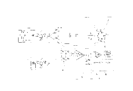
Fig. 6 illustrates a device according to the present invention, with a
preferred configuration of
the comparison unit 4 and the voltage source Uq, as well as a conversion unit
5 which here
is an integral component of the current source lq. The comparison unit 4 here
represents a
resistor bridge circuit that is connected to the first operating potential
Ub1, the second oper-
ating potential Ub2, and the control point C. For this purpose, over a first
resistor bridge
branch, the first operating potential Ub1 is connected in series via a first
resistor R1 to a sec-
ond resistor R2 with the second operating potential Ub2. A second resistor
bridge branch
connects the control point C to the second operating potential Ub 2 over a
third resistor R3
and a fourth resistor R4 that is connected in series. The differential
potential dU between the
predetermined potential Ux and the actual potential Uxist is applied between
the connection
point of the first resistor R1 and the second resistor R2 and the connection
point of the third
resistor R3 and the fourth resistor R4, whilst the resistors R1, R2, R3, R4
are sized accord-
ingly. In order to achieve a predetermined potential of Ux=(Ub1-Ub2)/2, a size
of, for exam-
ple, R2=R3=R4=(1/3)R1 would be required. It shall be readily understood that
the predeter-
mined potential Ux could also be predetermined externally, for example, by
regulatable volt-
age sources. Implementation through connections to the operating potentials
Ub1, Ub2
-8-
CA 2968179 2017-05-25
proves especially simple, however. Also present in fig. 6 are optional filter
capacitors Cb1,
Cb2 between the first operating potential Ub1/second operating potential Ub2,
respectively,
and the control point C. The differential potential dU is delivered from the
comparison unit 4
to the conversion unit 5. The conversion unit 5 converts the differential
potential dU into a
predetermined current lx. The conversion unit 5 may be realized by a PI
controller, e.g., de-
picted in fig. 6 by an operational transconductance amplifier (OTA) with an
output-side RC
element to ground. For this purpose, the differential potential dU is
connected between an
inverting input IV of the operation transconductance amplifier OTA and the non-
inverting in-
put NIV of the operation transconductance amplifier OTA. The operational
transconductance
amplifier OTA delivers a current lx to be specified, which is proportional to
the differential
potential dU, at the output that is connected to ground by means of the RC
circuit. The volt-
age at the capacitor Ca rises with the integral of the current lx to be
specified, and the volt-
age at the resistor Ra is proportional to the current lx to be specified. It
shall be readily un-
derstood that, alternatively, it would also be possible to use, for example,
an OPV circuit hay-
ing a capacitor and a serial resistor as feedback to the inverting input as
the PI controller.
Another capacitor for attenuating high-frequency currents may also be provided
parallel to
the capacitor and the resistor. Furthermore, a sensor S in this configuration
does not mea-
sure the actual potential Uxist, but rather the actual current lxist through
the control point C.
Thus, the sensor S can be easily realized as a shunt. A current controller 53
compares the
predetermined current lx and the actual current lxist obtained from the sensor
S, and deter-
mines the differential current. The current controller 53 is preferably
configured as a PI con-
troller. In addition to the current controller 53, the current source lq in
this configuration is
composed of a choke D and a voltage source Uq, which, in turn, is composed of
a driver half
bridge 6 that is controlled by a PWM module PWM and obtains the control
voltage UPMWM_IN
from the current controller 53 in accordance with the differential current.
PWM stands for
pulse width modulation, which is well known. Thus, the control voltage UpwmiN
is generated
by the current controller 53, and the PWM module PWM controls the driver half
bridge 6 so
that the differential current is regulated to zero. Advantageously, the
current controller 53 has
a current pre-controller having a current pre-control input through which the
pre-control cur-
rent Ivor flows. This current pre-controller is used to discharge the control
unit 3, here, in par-
ticular, the PI controller or operation transconductance amplifier OTA. With a
pre-controller, a
control variable is applied in a known manner with a value that is independent
of the states of
the control loop and resulting measurements, thus making it possible to take
into account the
control value need to be expected as a result of the set value profile. The
pre-control current
Ivor of the current pre-controller may be calculated with the aid of a model,
e.g., via the node
rule in the control point C. In this case, for example, the sum of all of the
coil currents 11_1 ,
ILn would correspond to the negative pre-control current -Ivor, as illustrated
also in fig. 6. The
-9-
CA 2968179 2017-05-25
driver half bridge 6 is composed here of two semiconductor switches 61, 62
connected in se-
ries. Advantageously, the upper semiconductor switch 61 connects the first
operating poten-
tial Ub1 to the second semiconductor switch 62, which, in turn, is connected
to the second
operating potential Ub2. The choke D connects the control point C to the
connection point
between the first semiconductor switch 61 and the second semiconductor switch
62 of the
driver half bridge 6. The PWM module PWM switches, with a Hi signal, the first
semiconduc-
tor switch 61, which thereby applies the first operating potential Ub1 to the
choke D; likewise,
with a Lo signal, the second operating potential Ub2 is applied to the choke
D. Thus, a volt-
age U is applied in accordance with the control voltage UpwmiN determined by
the current
controller 53 to the choke D, which in turn affects the actual current lxist
in the control point
C. The choke D integrates the rectangular voltage 7 and generates a triangular
actual current
lxist that has been smoothed. The semiconductor switches 61, 62 of the driver
half bridge
are advantageously configured as GaN (gallium nitride) switches. This
technology enables
switching frequencies in the MHz range, whereby a choke D with lower
inductance and thus
lower size can be used.
Advantageously, m>1 - where m is a positive integer - parallel driver half
bridges 6 are used
in order to reduce the waviness and therewith the current ripples of the
actual current lxist,
as shown in fig. 7 with the example of three parallel driver half bridges 6.
This also creates
the need form chokes D1, D2, D3, which must each have an inductance an m-th as
great as
the inductance of the single-phase configuration. The step response of the
actual current
lxist makes it clear that the actual current lxist rises m times as quickly
with m parallel-con-
nected inductances, and thus the predetermined current lx can be achieved
faster. The main
advantage in using a plurality of driver half bridges 6, however, lies in the
reduction of the
generated power loss. Because the power loss is known to be proportional to
the square of
the actual current lxist, for example, tripling the actual current lxist
brings about a reduction
of the power loss by a factor of nine. As a matter of course, m current
controllers 531, 532,
533 and current sources 1q1, 1q2, 1q3 are also necessary. The current sources
1q1,1q2,1q3
are controlled so as to deliver currents i1, i2, i3 with a phase shift of 360
/m, which are ap-
plied to the control point C, leading as a sum to the actual current lxist in
the control point C.
Fig. 7 represents a configuration with m=3 driver half bridges 601, 602, 603
and m=3 current
sources Iq1,1q2,1q3. The m=3 current sources are composed of m=3 chokes D1,
D2, D3,
and m=3 voltage sources Uq1, Uq2, Uq3; the voltage sources Uq1, Uq2, U3 are,
in turn,
composed of m=3 PWM modules PWM1, PWM2, PWM3 and m=3 driver half bridges 601,
602, 603. Provided that the m=3 driver half bridges 601, 602, 603 are
identically, even one
sensor S would theoretically be sufficient for acquiring the actual current
lxist. Because this
ideal case of absolutely identical driver half bridges 601, 602, 603 (and
chokes D1, 02, D3,
and so forth) typically does not occur in actual practice, fig. 7 illustrates
the general case of
-10-
CA 2968179 2017-05-25
m=3 sensors S1, S2, S3. The conversion unit 5 is not an integral component of
the current
sources lq1, 12, 1q3 in the configuration according to fig. 7. It would also
be conceivable to
configure the conversion unit 5 as an integral component of the current
sources Iq1,1q2, 1q3,
as in the configuration according to fig. 6, wherein, however, three
conversion units 5 would
then be necessary.
Fig. 8a illustrates the behavior of the m=3 currents i1, i2, i3 and the
resulting actual current
lxist with the use of m=3 current sources Iq1,1q2, 1q3 without phase shift.
The original rectan-
gular profiles of the voltages U1, U2, U3 generated by the voltage sources
Uq1, Uq2, Uq2
are integrated by the m=3 chokes D1, D2, D3 into triangular current profiles
of the m=3 cur-
rents i1, i2, 13. Fig. 8a depicts a control with three driver half bridges
601, 602, 603 without
phase shift (corresponding qualitatively to a control with one driver half
bridge 601, 602, 603
that delivers the actual current lxist). Fig. 8b shows that with a control of
the m=3 currents i1,
i2, i3 that is phase-shifted by 360 /3=120 , the current ripples of the actual
current lxist are
one-ninth as great as with a non-phase-shifted control. With a non-phase-
shifted control, the
current ripples of the actual current lxist are three times as great as a peak
current of a
phase 1, whereas the ripple current of the actual current lxist with phase-
shifted control is (5/3
- 4/3)1, which corresponds to a third of the peak current of a phase I.
If the application of the actual current lxist is performed through m phase
currents i1, i2, i3 in
m phases, then it is also possible to switch the m phase currents i1, i2, i3
partially or entirely
on or off in accordance with the differential current or the control voltage
Upwm_IN resulting
therefrom, as illustrated schematically in fig. 9. Each of the m current
sources lq may deliver
a maximum phase current i1max, i2max, i3max, which are identical in fig. 9.
The maximum
actual current lxistmax that can be delivered from the control unit 3 to the
control point C is
accordingly m times as high, provided that the maximum phase currents i1 max,
i2max,
i3max are of equal magnitude; otherwise, the maximum deliverable actual
current lxistmax
results from the sum of the phase currents ii max, i2max, i3max. If an actual
current lxist of
zero is sent out due to a differential current of zero, or the resulting
control voltage UPWM_IN,
then all of the current sources lq are switched off, in order to keep a
predetermined potential
of Ux. If the actual potential Uxist rises or falls beyond a certain
threshold, a phase current II,
i2, i3 is connected thereto. If a predetermined current lx that exceeds the
maximum phase
current i1max, i2max, i3max is required, then a second phase current i1, 12,
i3 must be con-
nected thereto; if the predetermined current lx is below a certain threshold,
then a phase
current i1, i2, i3 may be switched off, and so forth. Once a phase current i1,
i2, i3 is con-
nected thereto, the proportional component of the conversion unit 5 rises so
that the actual
current lxist falls immediately. In fig. 9, the first phase (first phase
current i1) is active (range
1P); first the second phase (second phase current i2, range 2P) and then the
third phase
(third phase current i3 activated, range 3P), and then first the third phase
(range 2P) and
-11-
CA 2968179 2017-05-25
then the second phase (range 1P) and finally even the first phase are switched
off. Zero ac-
tive phases mean a discontinuous drive, which is characterized as range OP in
fig. 9.
-12-