Note: Descriptions are shown in the official language in which they were submitted.
SUPERCONDUCTING SWITCH SYSTEM
[0001]
TECHNICAL FIELD
[0002] The present invention relates generally to superconducting circuits,
and
more particularly to a superconducting switch system.
BACKGROUND
[0003] Conventional microwave mechanical, electro-mechanical, and
electronic
switches may not be compatible with on-chip integration and cryogenic
operation of
superconducting electronic circuits, because of incompatible fabrication
processes and
high power dissipation. Likewise, tunable filters that are commonly realized
by use of
either active components such as voltage-variable capacitors i.e. varactors,
mechanical
drivers, or ferroelectric and ferrite materials, are not easily controllable
by signal levels
that can be generated with single flux quantum (SFQ) technologies, and many
are not
operable at cryogenic temperatures. While superconducting microwave filters,
both
fixed and tunable, have been previously realized using both high temperature
and low
temperature superconductors, their use in switching applications suffered from
high
return loss, limited usable bandwidth, and poor out-of-band off-state
isolation.
SUMMARY
[0004] In one example, a superconducting switch system is provided that
comprises a filter network having an input portion and an output portion, and
a variable
inductance coupling element that couples the input portion to the output
portion. The
variable inductance coupling element has a first inductance state that allows
a desired
portion of an input signal to pass from the input portion to the output
portion as an
output signal, and a second inductance state that suppresses the input signal
from
passing from the input portion to the output portion. The superconducting
switch
-1-
CA 2968827 2018-10-02
CA 02968827 2017-05-24
WO 2016/094045 PCT/US2015/061315
system further comprises a switch controller configured to control the
switching of the
variable inductance coupling element between the first inductance state and
the second
inductance state.
[0005] In another example, a superconducting switch system comprises a
filter
network having an input terminal and an output terminal, and a Superconducting
Quantum Interference Device (SQUID) coupled between the input terminal and the
output terminal. The SQUID includes a Josephson junction, a first inductor
coupled to a
first end of the Josephson junction, and a second inductor coupled to a second
end of
the Josephson junction with opposing ends of the first and second inductors
being
connected to a common potential to form a superconducting loop. The
superconducting
switch system also includes a switch controller configured to control an
amount of
induced current through the superconducting loop to switch the Josephson
junction
between a first inductance state in which a desired bandwidth portion of an
input signal
provided at the input terminal is provided at the output terminal, and a
second
inductance state in which the desired bandwidth portion of the input signal
provided at
the input terminal is suppressed from passing to the output terminal.
[0006] In yet a further example, a method is provided of providing a
superconducting switch system. The method comprises determining a desired pass-
band output for passing a desired bandwidth portion of an input signal to an
output of a
superconducting switch, determining a band-pass filter network topology for
the
superconducting switch, and determining a radio frequency (RF) SQUID insertion
point
in the band-pass filter. The SQUID comprises a first inductor coupled to a
variable
inductance coupling element on a first end and a second inductor coupled to
the
variable inductance coupling element on a second end in a superconducting
loop. The
method further comprises determining one or more input resonator and one or
more
output resonator component values for providing the superconducting switch,
and
building a superconductor switch system that includes the superconducting
switch. The
superconductor switch comprises the one or more input resonators, the one or
more
output resonators and the SQUID. The superconductor switch system further
comprises a bias inductor coupled to the SQUID and a switch controller that
switches
-2-
CA 02968827 2017-05-24
WO 2016/094045 PCT/US2015/061315
an amount of current through the bias inductor and induced in the SQUID to
change the
superconductor switch system between an 'ON' state and an 'OFF' state.
BRIEF DESCRIPTION OF THE DRAWINGS
[0007] FIG. 1 illustrates an example of a superconducting switch system.
[0008] FIG. 2 illustrates another example of a superconducting switch
system.
[0009] FIG. 3 illustrates a graph of transmission and reflection
scattering 5-
parameters versus frequency of the simulated response of the filter of FIG. 2
in the 'ON'
state.
[0010] FIG. 4 illustrates a graph of transmission and reflection
scattering 5-
parameters versus frequency of the simulated response of the filter of FIG. 2
in the
'OFF' state.
[0011] FIG. 5 illustrates a WRSpice simulation that outputs a graph of an
output
response versus time for the filter switch of FIG. 2.
[0012] FIG. 6 illustrates a graph of signal transmission through the
switch versus
frequency at a drive power of -90 dBm.
[0013] FIG. 7 illustrates a graph of power of signal transmission through
the
switch in the 'ON' state at a single frequency as a function of input power.
[0014] FIG. 8 illustrates a schematic diagram of a generic coupled
resonator filter
using inductive K-inverters.
[0015] FIG. 9 illustrates a block schematic diagram of another example of
a
superconducting switch system.
[0016] FIG. 10 illustrates a graph of transmission and reflection
scattering 5-
parameters versus frequency of the simulated response of the filter of FIG. 9
in the 'ON'
state.
[0017] FIG. 11 illustrates a graph of transmission and reflection
scattering 5-
parameters versus frequency of the simulated response of the filter of FIG. 9
in the
'OFF' state.
[0018] FIG. 12 illustrates a schematic of a 3rd order Chebyshev prototype
that can
be employed in a wide-bandwidth switch.
-3-
CA 02968827 2017-05-24
WO 2016/094045 PCT/US2015/061315
[0019] FIG. 13 illustrates a graph of transmission and reflection S-
parameters
versus frequency of the simulated response of a filter of FIG. 12 configured
as a wide-
bandwidth switch in the 'ON' state.
[0020] FIG. 14 illustrates a graph of transmission and reflection S-
parameters
versus frequency of the simulated response of the filter of FIG. 12 configured
as a wide-
bandwidth switch in the 'OFF' state.
[0021] FIG. 15 illustrates a method for providing a superconducting switch
system.
DETAILED DESCRIPTION
[0022] The present disclosure relates generally to superconducting
circuits, and
more particularly to a superconducting switch system. A superconducting switch
system can include a variable inductance coupler (also referred to as variable
inductance coupling element) that couples and decouples sections of a filter
network. In
one example, the variable inductance coupler is an element of a
Superconducting
Quantum Interference Device (SQUID). The SQUID can include a first inductor
and a
second inductor coupled to opposite sides of a variable inductance coupler all
arranged
in a superconducting loop. The variable inductance coupler can be, for
example, a
Josephson junction that has an inductance that can be varied based on a
current
flowing through the Josephson junction. The current flowing through the
Josephson
junction can be induced based on a flux applied to the SQUID by, for example,
a bias
element.
[0023] In one example, the Josephson junction can have a first inductance
when
no current or a low current is induced in the SQUID, and a second inductance
when a
current or a higher current is induced in the SQUID that is at a predetermined
threshold.
The predetermined threshold current induced in the SQUID can be a result of
applying a
flux to the SQUID from a bias element, for example, greater than about 0.1
c130 and less
than about 0.45 430, where c130 is equal to a flux quantum. The first
inductance can be
the passive inductance of a Josephson junction (e.g., h/2e * 1/1c, where his
the reduced
Planck's constant, e is the elementary charge and lc is the critical current
of the
Josephson junction) when no induced current flows through the Josephson
junction.
-4-
CA 02968827 2017-05-24
WO 2016/094045 PCT/US2015/061315
This allows for coupling between a first section of a filter network and a
second section
of the filter network, such that the superconducting switch system is in an
'ON' state
allowing passing of a desired bandwidth portion of an input signal. The second
inductance (e.g., large inductance value) can provide decoupling between the
first and
second section of the filter network such that the superconducting switch
system is in an
OFF' state suppressing the input signal.
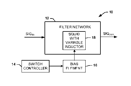
[0024] FIG. 1 illustrates an example of a superconducting switch system
10. The
superconducting switch system 10 can be implemented in any of a variety of
superconducting circuit systems to provide switch control of an input signal
SIGIN. As
an example, the input signal SIGIN can be a microwave signal that is
implemented in a
control scheme for a quantum circuit, such as performing a gate or a readout
operation
on a qubit. As another example, the input signal SIGIN can be a signal pulse
or another
type of signal. The superconducting switch system 10 can provide a band-pass
filtered
output signal SIGour that can corresponds to a desirable portion (e.g.,
particular
frequency bandwidth) of the input signal SIGIN when the superconducting system
is an
'ON' state (i.e., pass state). Additionally, all of the spectrum of the input
signal SIGN
can be suppressed or blocked such that none of the desired portion of the
input signal
SIGIN is provided as the output signal when in an 'OFF' state (i.e.,
suppressed state).
The superconducting switch system 10 includes a filter network 12 having one
or more
impedance components (i.e., capacitors, resistors, inductors) for configuring
an input
portion of the filter network 12 as one or more input resonators, and an
output portion of
the filter network 12 as one or more output resonators. At least one of the
one or more
input resonators and output resonators can be implemented as short-terminated
transmission line stubs.
[0025] The filter network 12 also includes a SQUID 18 with a variable
inductance
coupler (e.g., Josephson junction). The SQUID 18 also includes one or more
components that operate both as components of a superconducting loop of the
SQUID 18, and impedance components of the one or more input and/or the one or
more output resonators. A bias element 16 is inductively coupled to the SQUID
18 to
induce current in the SQUID 18. A change in the current induced in the SQUID
18 can
result in a change in inductance of the variable inductance coupler.
-5-
CA 02968827 2017-05-24
WO 2016/094045 PCT/US2015/061315
[0026] For example, the inductance of the variable inductance coupling
element
can be changed to a first inductance state, for example, when substantially no
induced
current or a low induced current is induced in the superconducting loop of the
SQUID 18, such that the inductance of the variable inductance coupling element
is low.
When the variable inductance coupling element is in the first inductance
state, the first
portion of the network is coupled to the second portion of the filter network
and the
superconducting switch system 10 is in the 'ON' state. Alternatively, the
inductance of
the variable inductance coupling element can be changed to a second inductance
state,
for example, when a substantial current (e.g., caused by induction of a
substantial
fraction of half of a flux quantum in the SQUID) is induced in the
superconducting loop
of the SQUID 18, such that the inductance of the variable inductance coupling
element
is high. When the variable inductance coupling element is in a high inductance
state,
the first portion of the network is decoupled from the second portion of the
filter network
and the superconducting switch system 10 is in the 'OFF' state. The bias
element 16
can be controlled by a switch controller 14 that controls an amount of bias
current to the
bias element 16, which in turn, controls an amount of flux applied to the
SQUID and an
amount of current induced in the SQUID 18 and flowing through the variable
inductance
coupler.
[0027] FIG. 2 illustrates an example of a superconducting switch system 30
having a filter network 32 configured as a single-pole-single-throw (SPST)
microwave
switch. In the example of FIG. 2, a two-section coupled-resonator band-pass
filter is
embedded with a radio frequency SQUID 34 having a tunable inductance coupler
in the
form of a Josephson junction J1. The SQUID 34 can include a first inductor L1
and a
second inductor L2 coupled to opposite sides of the Josephson junction J1 with
opposing
ends of the first and second inductor coupled to a common potential to form a
superconducting loop. The first inductor L1 can be employed to form an input
pole along
with other components of an input resonator of the band-pass filter, and the
second
inductor L2 can be employed to form an output pole along with other components
of an
output resonator of the band-pass filter. In the present example, the input
resonator is
formed of a first capacitor C, an inductor Ls1 and the first inductor
-6-
CA 02968827 2017-05-24
WO 2016/094045 PCT/1JS2015/061315
[0028] An input signal (SIGN) is provided at an input terminal (IN) to the
input
resonator through an input coupling capacitor Cc. The output resonator is
formed of a
second capacitor Cl, an inductor Ls2 and the second inductor L2. An output
signal
(SIGouT) can be provided at an output terminal (OUT) from the output resonator
through
an output coupling capacitor Coc. The input coupling capacitor Cic and the
output
coupling capacitor Co c assure that the current flowing through the
superconducting loop
of the SQUID 34 is isolated such that it remains in the SQUID 34 and does not
flow to
other parts of the circuit.
[0029] The Josephson junction J1 has an inductance that can be varied based
on
the induced current flowing through the Josephson junction J1. A bias inductor
LB is
inductively coupled to the SQUID 34 to apply flux to the SQUID 34 and to
induce current
in the SQUID 34. The bias inductor LB can be controlled by a switch controller
36 that
controls an amount of bias current IB to the bias inductor LB, which in turn,
controls an
amount of induced current liND in the SQUID 34 and flowing through the
Josephson
junction J1. The Josephson junction J., can have a first inductive state when
no current
or a low current is induced in the SQUID, such that the input resonator is
coupled to the
output resonator of the filter network 32 through the Josephson junction J1.
The
Josephson junction J1 can have a second inductive state such when a
predetermined
higher current is flowing through the Josephson junction J1. The second
inductive state
is a high inductance that essentially decouples the input resonator from the
output
resonator and suppresses the input signal from being provided as an output
signal.
[0030] In the example of FIG. 2, when a first flux is applied to the RF
SQUID
loop 34 defined by Josephson junction J1 and inductors L1 and L2, a first
induced
current flows through the junction J1 resulting in junction J1 having a first
inductance
value. This first inductance state can be designed such that the circuit as a
whole
functions as a band-pass filter with low insertion loss in its pass-band. The
superconducting switch system 10 is then said to be in an 'ON' state. When a
second
flux is applied to the RF SQUID loop, a second higher current is induced in
the junction
J1 causing its inductance value to increase, driving the inductive coupling
between the
input and output stages to zero. The two sections of the band-pass filter
formed from
the input resonator and the output resonator are then decoupled from each
other, such
-7-
CA 02968827 2017-05-24
WO 2016/094045 PCT/US2015/061315
that the filter circuit as a whole has a high return loss at all frequencies
because the
filter becomes reflective. The superconducting switch system 30 is then said
to be in an
'OFF' state. In one example, the first applied flux is at or close to zero,
and the second
applied flux is an appreciable fraction of half a flux quantum (e.g., about .1
430 to
about .45 (1)o).
[0031] FIGS. 3-4 illustrate graphical responses of simulations of the
filter
switch 32 of FIG. 2 using Agilent Advanced Design System (ADS). In this
simulation,
the Josephson junction J1 is treated as a linear inductor corresponding to its
Josephson
inductance at low drive power. The simulated component values are Ls1=Ls2=60
pH,
L1=L2=169 pH, C1.C2=1.19 pF, Cic=Coc=0.659 pF, and the inductance
corresponding
to the junction LA=375pH. FIG. 3 illustrates a graph 40 of gain versus
frequency
showing S21 and S11 of the filter switch 32 in the 'ON' state, showing a 2 GHz
pass-band
centered about 10 GHz. The S21 parameter is shown in the signal transmission
plot 42
and the Sii parameter is shown in the signal reflection plot 41. The filter
switch 32 is
then turned to the 'OFF' state by applying a predetermined flux to the RF
SQUID loop,
causing the inductance of junction J1 to increase. The increasing effective
inductance
of the RF SQUID is modeled in a graph 45 illustrated in FIG. 4, which
illustrates gain
versus frequency, by raising the value of the junction inductance by a factor
of 30. The
S21 parameter is shown in the signal transmission plot 46 and the Siiparameter
is
shown in the signal reflection plot 47. An overall suppression of the S21
parameter, and
in particular a 20 dB reduction of the transmission in the pass-band is
realized.
[0032] FIG. 5 illustrates a WRSpice simulation that outputs a graph 50 of
an
output response versus time for the filter switch 32 of FIG. 2. All component
values are
the same as indicated above. Flux bias is applied to the RF SQUID by the
current lb
and the bias component LB via the switch controller 36. The input waveform is
a 10
GHz sinusoid at a power of -120 dBm, the flux bias waveform 54 is piecewise
linear in
shape, and the voltage at the load termination (filter output) is shown as
output
waveform 52. As shown, in response to a flux bias sweep from 0 to 0.37 Iv the
output
voltage changes by a factor of over 80, corresponding to over 30 dB switch
ON/OFF
ratio.
-8-
CA 02968827 2017-05-24
WO 2016/094045 PCT/US2015/061315
[0033] A harmonic-balance simulation was also performed in ADS on the
circuit
of FIG. 2, treating the Josephson junction as a nonlinear inductor. This
simulation
captures the power dependence of the switch performance expected in circuits
containing Josephson junctions. FIG. 6 illustrates a graph 60 of signal
transmission
through the switch versus frequency at a drive power of -90 dBm. FIG. 7
illustrates a
graph 62 of power of signal transmission through the switch in the 'ON' state
at a single
frequency as a function of input power as well as the large-amplitude S21. The
simulation as illustrated in FIG. 6 indicates that the switch can handle input
powers up
to -90 dBm without degradation to its 'ON' state response. The off state
isolation begins
to degrade at approximately -80 to -85 dBm according to transient analysis of
the circuit
model. The applied flux at the 'OFF' state can be adjusted to improve switch
performance at these power levels.
[0034] The utilization of an RF SQUID embedded in a filter network to
provide a
superconducting switch system has been illustrated for one particular example.
However, the utilization of an RF SQUID embedded in a filter network to
provide a
superconducting switch system can be employed in a variety of different filter
topologies. For example, a lumped-element, coupled-resonator topology, can be
employed where resonators having a frequency that coincides with the center
frequency
of the filter are coupled via admittance (J) or impedance (K) inverters, and
the coupling
coefficients of the inverters are related to tabulated filter prototypes to
realize a desired
response (e.g. Chebyshev, max-flat, etc.). At least one of the inverters can
be
implemented as an inductive network having a "pi" circuit topology. The series
inductor
of the pi-section inverter can be replaced with a Josephson junction so that
the inverter
becomes an RF SQUID.
[0035] For example, FIG. 8 illustrates a schematic diagram of a generic
coupled
resonator filter 70 using inductive K-inverters. The circuit components can be
computed
according to tabulated filter prototypes to give a desired response. The
circuit 70 of
FIG. 8 can be modified by commuting the series inductors and capacitors,
forming T-
networks of inductors between each capacitor. The T-networks can then be
transformed to pi-networks to integrate the RF SQUID design, replacing at
least one of
the resulting series inductors with a Josephson junction.
-9-
CA 02968827 2017-05-24
WO 2016/094045 PCT/US2015/061315
[0036] As an example, a circuit schematic of another example of a
superconducting switch system 80 is shown in FIG. 9 for the filter type of
FIG. 8 with an
order of 2, where an RF SQUID loop 84 is formed by junction JA and inductors
LA and
LB. The inductor LA can be employed to form an input pole of an input
resonator along
with inductor Hi and capactitor CA. The inductor LB can be employed to form an
output
pole of an output resonator along with inductor LH2 and capactitor CB. An
input signal
(SIGN) is provided at an input terminal (IN) to the input resonator through an
input
coupling inductor LA. An output signal (SIGouT) can be provided at an output
terminal
(OUT) from the output resonator through an output coupling inductor LJ2. The
capacitor
CA and the capacitor CB also act as coupling capacitors to isolate the induced
current
that runs through the superconducting loop of the RF SQUID 84 from other parts
of the
circuit.
[0037] A bias inductor LB2 is inductively coupled to the SQUID 84 to induce
current in the SQUID 84. The bias inductor LB2 can be controlled by a switch
controller 86 that controls an amount of bias current IB2 to the bias inductor
LB2, which in
turn, controls an amount of induced current liND in the SQUID 84 and flowing
through
the Josephson junction JA. The Josephson junction JA has an inductance that
can be
varied based on the induced current flowing through the Josephson junction JA.
The
Josephson junction JA can have a first inductance state when no current or a
low
current is flowing through the SQUID 84, such that the desired portion of the
input signal
passes through the filter network 82 through the Josephson junction JA to be
provided
as an output signal. The Josephson junction JA can have a second inductance
state
that essentially decouples the input portion of the filter network 82 from the
output
portion of the filter network 82 suppressing the input signal from being
provided as an
output signal. In this particular example, the circuit parameters are LHi
=LH2=104pH,
LA=LJ2=46.0pH, LA=LB=132pH, CA=CB=1.74pF, and the junction effective
inductance
Lj_A=566pH corresponding to a critical current 10=0.58pA. FIG. 10 illustrates
a graph 90
of gain versus frequency of the simulated response of this filter in the 'ON'
state. The
S21 parameter is shown in the signal transmission plot 92 and the S11
parameter is
shown in the signal reflection plot 91. FIG. 11 illustrates a graph 95 of gain
versus
frequency of the simulated response of this filter in the 'OFF' state. The S21
parameter
-10-
CA 02968827 2017-05-24
WO 2016/094045 PCT/US2015/061315
is shown in the signal transmission plot 96 and the S11 parameter is shown in
the signal
reflection plot 97.
[0038] As another example, a 40% bandwidth switch 100 can be provided based
on a 3rd order Chebyshev prototype, having the topology shown in FIG. 12.
Inductor L1
in FIG. 12 can be replaced with a Josephson junction, and an RF SQUID is then
formed
by the combination of L1 and the shunt inductances of resonators PLC8 and PLC
9.
FIG. 13 shows a graph 110 of the results of an S-parameter simulation of this
design in
an 'ON' state with the Josephson junction being approximated by a linear
inductor. The
S21 parameter is shown in the signal transmission plot 111 and the S11
parameter is
shown in the signal reflection plot 112. FIG. 14 shows a graph 120 of the
results of an
S-parameter simulation of this design in an 'OFF' state with the Josephson
junction
being approximated by a linear inductor. The S21 parameter is shown in the
signal
transmission plot 121 and the S11 parameter is shown in the signal reflection
plot 122.
[0039] In summary, an RF SQUID tunable inductance coupler can be embedded
in a coupled-resonator band-pass filter to implement a microwave switch, with
better
than 20 dB on/off ratio, up to 40% bandwidth, and input powers up to -85 dBm.
The
switch is actuated by application of flux to the RF SQUID in a manner that is
compatible
with SFQ control.
[0040] In view of the foregoing structural and functional features
described
above, a methodology in accordance with various aspects of the present
invention will
be better appreciated with reference to FIG. 15. While, for purposes of
simplicity of
explanation, the methodology of FIG. 15 is shown and described as executing
serially, it
is to be understood and appreciated that the present invention is not limited
by the
illustrated order, as some aspects could, in accordance with the present
invention,
occur in different orders and/or concurrently with other aspects from that
shown and
described herein. Moreover, not all illustrated features may be required to
implement a
methodology in accordance with an aspect of the present invention.
[0041] FIG. 15 illustrates a method 150 for providing a superconducting
switch
system. The methodology begins at 152, where a desired pass-band output is
determined for passing an input signal through a switch as an output signal or
suppressing the input signal from passing to the output of the switch. At 154,
a desired
-11-
CA 02968827 2017-05-24
WO 2016/094045 PCT/US2015/061315
band-pass filter topology is determined for providing a superconducting
switch. As
previously discussed, a variety of different filter topologies can be selected
from to
provide a superconducting switch system based on a desired pass-band output
response. At 156, an RF SQUID insertion point is determined based on the
selected
filter topology. The methodology then proceeds to 158.
[0042] At 158, one or more input resonators and one or more output
resonator
component values are selected to provide the desired pass-band output based on
the
determined pass-band filter topology and RF SQUID insertion point. This
includes
assuring that the resonators include isolation capacitors to ensure that the
current
flowing through the SQUID does not flow into other parts of the circuit. The
SQUID can
include a first and second inductor coupled to opposite sides of a variable
inductance
coupling element (e.g., Josephson junction). At 160, the RF SQUID component
values
are determined based on the one or more output resonator component values and
the
desired pass-band output constrained by assuring the SQUID linear inductance
does
not exceed the inductance of the variable inductance element.
[0043] Assuring that the SQUID linear inductance does not exceed the
inductance of the variable inductance element, ensures that the potential of
the RF
SQUID is monostable. At 162, the superconducting switch system is built
including the
microwave switch with the above selected components, a bias inductor and a
switch
controller to drive the bias inductor into inducing a current in the SQUID
that can change
a value in the variable inductance coupling element between a pass state for
passing a
desired pass-band of an input signal to a suppressed state for suppressing a
the input
signal.
[0044] What have been described above are examples of the invention. It is,
of
course, not possible to describe every conceivable combination of components
or
methodologies for purposes of describing the invention, but one of ordinary
skill in the
art will recognize that many further combinations and permutations of the
invention are
possible. Accordingly, the invention is intended to embrace all such
alterations,
modifications, and variations that fall within the scope of this application,
including the
appended claims.
-12-