Note: Descriptions are shown in the official language in which they were submitted.
EXTERNAL DC OVERCURRENT ELECTRONIC TRIP UNIT FOR CIRCUIT
BREAKER
CROSS REFERENCE TO RELATED APPLICATION
[0001] This application claims the benefit of U.S. Provisional Application No.
62/344,444, filed
June 2, 2016.
BACKGROUND OF THE INVENTION
[0002] Field of the Invention
[0003] The present invention relates to DC circuit breakers found, for
example, on rapid transit
trains, and, more particularly, to an apparatus and method for controlling the
closed and open states
of the DC circuit breaker in a time-domain dependent manner.
[0004] Description of Related Art
[0005] Rapid transit systems are widely used for high-volume passenger
transportation. Rail
passenger train DC auxiliary subsystems are supplied power by a low voltage
power supply
(LVPS) at a voltage that typically varies between 24 volts and 110 volts.
Batteries are also used
to support important and essential loads under emergency conditions. An
advantage of using DC
power versus AC power is the possibility to distribute variable-frequency
drives near the loads
without any AC-to-DC conversion. DC auxiliary subsystems and DC distribution
in aircrafts, on
manned aerial vehicles, shipboards, commercial and industrial buildings, as
well as data centers is
being widely developed. Fault protection in DC systems is still a subject of
broad interest due to
the lack of standards compared to AC systems.
[0006] Circuit breakers are often preferred to fuses in railway vehicles
because the latter shown
thermal fatigue, cannot be controlled remotely, do not provide a means to
easily isolate circuits
during maintenance, and need to be replaced. Circuit breakers widely in use in
railway vehicles
include a thermomagnetic trip circuit. The rating of such circuit breakers is
selected to be high
enough to avoid false trip during emergency and maximum operating temperature
conditions.
However, under cold temperature conditions, especially outdoor rapid transit
systems, the
effectiveness of the thermomagnetic trip circuit, especially in the thermal
region, is reduced.
Moreover, the available fault current tolerance is generally limited. Because
of ratings and
tolerances on the trip curves of commercially available circuit breakers that
include
1
Date Recue/Date Received 2023-06-15
thermomagnetic trip circuits, it is possible during a short circuit, e.g., a
short between the positive
and the negative lines of a low voltage bus, that the trip curve will fall
into the thermal zone such
that the fault may last for many seconds, leading to hazardous conditions.
SUMMARY OF THE INVENTION
100071 Disclosed herein is, among other things, a circuit breaker that
includes the combination
of a prior art thermomagnetic trip circuit in combination with a shunt trip
coil operating under the
control of an electronic trip circuit in accordance with the examples
described herein. The use of
the electronic trip circuit in combination with the thermomagnetic trip
circuit aids in the rapid
detection of a fault current and the opening of one or more contacts of the
circuit breaker more
rapidly than the thermomagnetic trip circuit alone. The combination of the
thermomagnetic trip
circuit and the electronic trip circuit increases the protection performance
of the circuit breaker
against fault conditions appearing on the voltage bus lines.
[0008] Various preferred and non-limiting examples of the present invention
will now be
described and set forth in the following numbered clauses:
[0009] Clause 1: A DC circuit breaker includes at least one contact configured
to be coupled
between a source of DC power and a DC load. A thermomagnetic trip circuit is
operable in
accordance with a first time-current curve that defines: a first time-current
region (1TCR) where
the contact, starting in a closed state, remains in the closed state in
response to the contact being
exposed to a combination of current and time in the 1TCR, and a second time-
current region
(2TCR) where the contact, starting in the closed state, switches to an open
state in response to the
contact being exposed to a combination of current and time in the 2TCR. An
electronic trip circuit
is operable in accordance with a second time-current curve that defines a
third time-current region
(3TCR) where the contact, starting in the closed state, remains in the closed
state in response to
the contact being exposed to a combination of current and time in the 3TCR,
and a fourth time-
current region (4TCR) where the contact, starting in the closed state,
switches to the open state in
response to the contact being exposed to a combination of current and time in
the 4TCR. Each
combination of current and time comprises a total time that DC current flows
in the contact and a
level of the DC current flowing in the contact at said total time.
100101 Clause 2: The DC circuit breaker of clause 1, wherein at least a part
of the 1TCR and a
part of the 4TCR overlap and have time-current pairs or points in common.
3RZ2096-Utility Appin. approved for filing.DOCX 2
CA 2969281 2017-05-31
[0011] Clause 3: The DC circuit breaker of clause 1 or 2, further including a
current sensor
configured to sense the DC current flowing in the contact, wherein the
electronic trip circuit
includes a controller responsive to an output of the current sensor for
determining that at least one
combination of current and time falls in the 4TCR.
[0012] Clause 4: The DC circuit breaker of any one of clauses 1-3, wherein the
controller is
responsive to determining that said at least one combination of current and
time falls in the 4TCR
for causing the contact to switch from the closed state to the open state.
[0013] Clause 5: The DC circuit breaker of any one of clauses 1-4, wherein the
electronic trip
circuit includes: a converter configured to convert DC voltage on the DC bus
to a different level
DC voltage; and an energy storage for storing DC power at the different level
DC voltage for use
by the controller.
[0014] Clause 6: The DC circuit breaker of any one of clauses 1-5, wherein the
controller
includes a time over current detect circuit which determines, based on the
output of the current
sensor, that the level of the DC current flowing in the contact exceeds a
predetermined level and
the total time that must accumulate before the combination of current and time
is in the 4TCR.
[0015] Clause 7: The DC circuit breaker of any one of clauses 1-6, wherein the
controller
includes a level detector configured to detect when the sensed DC current
exceeds a predetermined
maximum level and, in response thereto, to cause the contact to switch from
the closed state to the
open state.
[0016] Clause 8: A method of controlling a DC circuit breaker comprising: (a)
sensing a level
of DC current flowing in at least one contact of the DC circuit breaker in a
closed state;
(b) accumulating an indication of the total time the DC current in step (a) is
sensed; (c) comparing
the accumulated indication in step (b) to a predetermined value or level; and
(d) in response to the
accumulated indication in step (b) exceeding the predetermined value or level,
causing the at least
one contact to switch from the closed state to an open state.
[0017] Clause 9: The method of clause 8, wherein the accumulated indication is
an
accumulated charge on a capacitor.
[0018] Clause 10: The method of clause 8 or 9, wherein the capacitor is
charged with current
from a current source and the value of the charging current is based on the
level of the DC current
sensed in step (a).
3RZ2096-Utility Appin. approved for filing.DOCX 3
CA 2969281 2017-05-31
[0019] Clause 11: The method of any one of clauses 8-10, wherein step (b)
includes
accumulating the indication of the total time the DC current in step (a) is
sensed only when the
level of the DC current exceeds a predetermined value.
[0020] Clause 12: The method of any one of clauses 8-1 l , wherein at least
one of steps (b), (c),
and (d) is performed under the control of a programmed digital controller.
[0021] Clause 13: The method of any one of clauses 8-12, wherein the
programmed digital
controller includes one of the following operating under the control of
computer readable program
code: a microprocessor; or a digital signal processor (DSP).
[0022] Clause 14: The method of any one of clauses 8-13, further including:
causing the at
least one contact to switch from the closed state to the open state in
response to a temperature of
the DC circuit breaker exceeding a predetermined temperature.
[0023] Clause 15: The method of any one of clauses 8-14, further including:
causing the at
least one contact to switch from the closed state to the open state in
response to a magnetic field
produced by the DC current flowing in at least one contact exceeding a
predetermined value.
BRIEF DESCRIPTION OF THE DRAWINGS
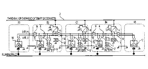
100241 Fig. 1 is a diagrammatic drawing of a five car rapid transit train
including a low voltage
bus running between the cars that is powered by low voltage power supplies
(LVPS) and batteries
for supplying electrical power to DC loads distributed throughout the cars and
including DC circuit
breakers to protect against fault conditions, such as a short circuit, that
may appear on the low
voltage bus;
[0025] Fig. 2 is a schematic drawing of a prior art circuit breaker including
a thermomagnetic
trip circuit;
[0026] Fig. 3 is a log-log graph of current versus time including first and
second example plots
of minimum and maximum tolerance operation of the example circuit breaker of
Fig. 2;
[0027] Fig. 4 is a schematic drawing of the circuit breaker and thermomagnetic
trip circuit of
Fig. 2 including a shunt trip coil that is controlled by an example electronic
trip circuit that receives
an indication of the current flowing in one or more contacts of the circuit
breaker via a current
sensor and, optionally, if provided, a differential current sensor;
[0028] Fig. 5 is a detailed schematic of the power supply, energy storage,
circuit breaker
(including shunt trip coil), and shunt trip circuit shown in Fig. 4;
3RZ2096-Utility Appin, approved for tiling.DOCX 4
CA 2969281 2017-05-31
=
[0029] Fig. 6 is a detailed schematic of the low pass filter (40) and
controller (DC current)
configured for processing the output of the current sensor shown in Fig. 4;
[0030] Fig. 7 is a log-log graph of current versus time including example
third and fourth plots
illustrating the operation of the controller (DC current) of Fig. 6 to control
the closed and open
state of one or more of the contacts of the circuit breaker of Fig. 4 in
accordance with either the
third plot or the fourth plot based on adjustments of resistors of the
controller (DC current) shown
in Fig, 6;
[0031] Fig. 8 is a log-log graph of current versus time including the first
plot of Fig. 3 and the
third plot of Fig. 7 reproduced thereon;
[0032] Fig. 9 is a detailed schematic of the optional low pass filter and the
optional controller
(differential current) of Fig. 4 configured to process the output of the
differential current sensor;
[0033] Fig. 10 is a schematic of the circuit breaker including the
thermomagnetic trip circuit
and shunt trip coil shown in Fig. 4 and including another example electronic
trip circuit that
includes a programmed digital controller to digitally process the output of
the current sensor and,
optionally, if provided, the differential current sensor; and
[0034] Fig. 11 is an example block diagram of the programmed digital
controller shown in
Fig. 10.
DESCRIPTION OF THE INVENTION
[0035] Various non-limiting examples will now be described with reference to
the
accompanying figures where like reference numbers correspond to like or
functionally equivalent
elements.
[0036] For purposes of the description hereinafter, the terms "end," "upper,"
"lower," "right,"
"left," "vertical," "horizontal," "top," "bottom," "lateral," "longitudinal,"
and derivatives thereof
shall relate to the example(s) as oriented in the drawing figures. However, it
is to be understood
that the example(s) may assume various alternative variations and step
sequences, except where
expressly specified to the contrary. It is also to be understood that the
specific example(s)
illustrated in the attached drawings, and described in the following
specification, are simply
exemplary examples or aspects of the invention. Hence, the specific examples
or aspects disclosed
herein are not to be construed as limiting.
[0037] With reference to Fig. 1, an example rapid transit train can include
cars Al, B2, C3, B4,
and A5. In an example, car Al can be the lead car and car A5 can be the
trailing car. Any one or
3RZ2096-Utility Appin. approved for filing.DOCX 5
CA 2969281 2017-05-31
number of the cars can include a propulsion system that can be operated in a
manner known in the
art to provide motive force to the train to move along running rails or other
closed pathway. The
rapid transit train can also include a DC auxiliary power system that receives
power from a third
rail or overhead catennary system 2 (hereinafter "third rail").
[0038] The train shown in Fig. 1 can include one or more low voltage power
supplies (LVPS) 4
which operate in a manner known in the art to step down the high voltage DC
power supplied by
third rail 2 to a lower voltage supplied to a low voltage bus 6 that runs
between the cars of the
train. In the illustrated example, cars B2, C3, and B4 each include LVPS 4 and
cars Al and A5
do not. However, this is not to be construed in a limiting sense since each
car may or may not
include an LVPS 4 depending on, for example, the need for an LVPS 4 in said
car.
[0039] The train can also include a number of batteries 8 for storage of DC
power supplied on
the low voltage bus 6. In an example, low voltage bus 6 can be a 32.5 volt DC
bus. However, this
is not to be construed in a limiting sense. Moreover, in the illustrated
example, cars B2, C3, and
B4 include batteries 8 and cars Al and A5 do not. However, this is not to be
construed in a limiting
sense since each car may or may not include a battery 8 as deemed suitable
and/or desirable by the
application.
[0040] In an example, each car can include one or more DC loads 10 coupled to
low voltage
bus 6 in parallel with the one or more batteries 8 and the one or more LVPS 4.
The train can
further include one or more ground fault detection circuits 12 coupled to low
voltage bus 6. In the
illustrated example, cars B2, C3, and B4 include ground fault detection
circuits 12. However, the
number and distribution of ground fault detection circuits in the cars of the
example train shown
in Fig. 1 can be determined by one of ordinary skill in the art.
[0041] In an example, the train shown in Fig. I can also include a number of
DC circuit
breakers 14 distributed at strategic locations on low voltage bus 6 and in-
line with each battery 8.
In the example train shown in Fig. 1, DC circuit breakers 14 are disposed on
low voltage bus 6 on
each end of cars B2 and B4. Moreover, a DC circuit breaker is positioned in-
line with each
battery 8. However, the positions of DC circuit breakers 14 in the train shown
in Fig. I are not to
be construed in a limiting sense.
[0042] With reference to Fig. 2 and with continuing reference to Fig. 1, each
circuit breaker 14
includes one or more contacts 16 (hereinafter "the contact(s) 16") operating
the control of a
thermomagnetic trip circuit 18 of circuit breaker 14 which is operative for
controlling the open and
3RZ2096-Utility Appin. approved for filing.DOCX 6
CA 2969281 2017-05-31
closed state of the contact(s) 16 in a manner known in the art. Specifically,
thermomagnetic trip
circuit 18 is configured to control the open and closed states of the
contact(s) 16 under tripping
conditions, namely, thermal and magnetic, which can act independently of each
other.
100431 Under the thermal trip condition, the release of contact(s) 16 from a
closed to an open
state varies inversely with the current flowing through the circuit breaker.
The thermal trip region
is intended for protection against continuous overload while allowing
momentary current surges.
A relatively large tolerance on detection time is generally specified due to
operating temperature
impact on the actual thermal detection mechanism (not shown).
[0044] In a magnetic trip condition, the release delay of the contact(s) 16
from a closed state
to an open state is constant when the current flowing is beyond the
instantaneous current trip value.
This trip mechanism is intended for protection against short-circuit. Circuit
breaker 14, including
thermomagnetic trip circuit 18 for controlling the release of one or more
contacts from a closed
state to an open state, is well known in the art.
[0045] With reference to Fig. 3 and with continuing reference to Figs. 1 and
2, example log-
log plots of current versus time of circuit breaker 14, including
thermomagnetic trip circuit 18,
includes a first example plot 20 that represents an example minimum tolerance
of thermomagnetic
trip circuit 18 and second example plot 22 that represents an example maximum
tolerance of
thermomagnetic trip circuit 18.
[0046] Referring to first plot 20, the range of current from approximately 300
amps to
1,760 amps represents the thermal trip region of thermomagnetic trip circuit
18 while above 1,760
amps represents the magnetic trip region of thermomagnetic trip circuit 18.
Referring to second
plot 22, between about 400 amps and 2,640 amps represents the thermal trip
region of
thermomagnetic trip circuit 18 while above 2,640 amps represents the magnetic
trip region of
thermomagnetic trip circuit 18. For each of the first plot 20 and second plot
22, the area of the
time-current region to the left of said plot (including the thermal trip
region of said plot) represents
a first time-current region (1TCR) while the area to the right of said plot
(including the magnetic
trip region) represents a second time-current region (2TCR). For example, with
respect to first
plot 20, point 24 (400 amps, 1 second) is in the 1TCR (and in the thermal trip
region) of first plot
20 while point 26 (1,000 amps, 10 seconds) is in the 2TCR (also in the thermal
trip region) of first
plot 20. With respect to second plot 22, point 26 is in the 1TCR (the thermal
trip region) of second
3RZ2096-Utility Appin. approved for filing.DOCX 7
CA 2969281 2017-05-31
plot 22 while point 28 (2,000 amps, 100 seconds) is in the 2TCR (also in the
thermal trip region)
of second plot 22.
100471 The large difference between minimum tolerance (first plot 20) and
maximum tolerance
(second plot 22) of the thermomagnetic trip circuit 18 may be unacceptable in
the environment of
the train shown in Fig. 1. This is because in the event of a fault current,
e.g., a short circuit between
the positive and negative lines of low voltage bus 6, the current flowing
through the short circuit
and, hence, on low voltage bus 6 can fall into the thermal region of the
thermomagnetic trip
circuit 18 and may last for several seconds, leading to a hazardous condition.
100481 Having described the prior art, the present invention will now be
described.
100491 With reference to Fig. 4, in an example, circuit breaker 14 can be
modified to include a
shunt trip coil 30 that is operative separately from thermomagnetic trip
circuit 18 to cause the
contact(s) 16 to move from a closed state to an open state under the control
of an electronic trip
circuit 32.
100501 In an example, electronic trip circuit 32 includes a power supply 34,
an energy storage
36, and a shunt trip circuit 38 shown in more detail in Fig. 5. Electronic
trip circuit 32 also includes
a low pass filter 40 and a controller 42 shown in more detail in Fig. 6.
Finally, electronic trip
circuit 32 can optionally include a second low pass filter 44 and a second
controller 46 shown in
more detail in Fig. 9.
100511 With reference to Fig. 5 and with continuing reference to Fig. 4, power
supply 34
includes an input capacitor 50 is connected to the positive and negative lines
of low voltage bus 6.
Power supply 34 includes a DC/DC converter 52 coupled to receive DC electrical
power from low
voltage bus 6 and input capacitor 50. In an example, DC/DC converter 52 is
operative in a manner
known in the art to convert DC voltage on low voltage bus 6 into a voltage
suitable for use by
shunt trip coil 30 to release the contact(s) 16 from a closed state to an open
state and for supplying
DC electrical power at a suitable level for the operation of other elements of
electronic trip circuit
32. In an example, the DC/DC converter 52 shown in Fig. 5 includes a
transformer 53 that includes
a primary winding 54, a first, secondary-winding 56, and a second, secondary-
winding 58.
100521 The example DC/DC converter 52 shown in Fig. 5 is a flyback converter
that includes
a flyback controller 60 and a switching element 62 (e.g., a transistor) which
are operative for
converting the DC input voltage from low voltage bus 6 and input capacitor 50
into an AC voltage
which is converted by transformer 53 into first and second AC voltages on
first and second
3RZ2096-Utility Appin. approved for filing.DOCX 8
CA 2969281 2017-05-31
secondary-windings 56 and 58 in a manner known in the art. The AC voltage
produced on first
secondary-winding 56 is rectified by diode 64 and stored in energy storage 36.
The AC voltage
output by second, secondary-winding 58 is rectified by a diode 66 and stored
on a capacitor 68 for
use by the one or more elements of electronic trip circuit 32 described
hereinafter. The
combination of second, secondary-winding 58, diode 66, and a capacitor 68
define a low voltage
power supply 69.
[0053] Energy storage 36 is connected to one end of shunt trip coil 30 the
other end of which
is connected to shunt trip circuit 38. In an example, shunt trip circuit 38
includes a switching
element 70, e.g., a transistor, coupled to control the flow of current through
shunt trip coil 30 under
the control of a current controller 72 in response to an output of an OR
circuit 48 (Fig. 4). In an
example, current controller 72 can include any suitable and/or desirable
circuitry that may be
required to convert the output of OR circuit 48 into a suitable control signal
for controlling the
on/off state of switching element 70. It is also envisioned that the output of
OR circuit 48 can be
used to directly control the on/off state of switching element 70.
[0054] The example DC/DC converter 52 shown in Fig. 5 is a flyback converter.
However,
this is not to be construed in a limiting sense since it is envisioned that
any suitable and/or desirable
topology or type of DC/DC converter 52 can be utilized. One example of another
suitable DC/DC
converter is a buck/boost converter. One skilled in the art can select a
suitable DC/DC converter
for use as the power supply 34 of electronic trip circuit 32. Accordingly, the
disclosure herein of
power supply 34, including DC/DC converter 52, is not to be construed in a
limiting sense.
[0055] With reference to Fig. 6 and with continuing reference to Figs. 4 and
5, a current
sensor 74, for example, a hall effect sensor, can be positioned to sense
current flowing on the
positive line of low voltage bus 6. An output of current sensor 74 can be
coupled to low pass filter
40 which, in a manner known in the art, low pass filters the output of current
sensor 74 and provides
the low pass filtered output to a controller (DC current) 42 via an optional
precision rectifier 76, if
provided.
[0056] Controller 42 includes a comparator 78 which compares the output
voltage of low pass
filter 40 or, if provided, precision rectifier 76 to a reference value set by
a resistor 80 which is
coupled between the Vcc output of the low voltage power supply 69 and ground.
More
specifically, comparator 78 operates in a manner known in the art comparing
the voltage at a first
3RZ2096-Utility Appin. approved for tiling.DOCX 9
CA 2969281 2017-05-31
input 82 output by low pass filter or, if provided, precision rectifier 76 to
a second voltage at a
second input 84 of comparator 78 provided via resistor 80.
100571 For the purpose of describing logic levels herein, a positive logic
convention will be
assumed wherein a high, positive, or logical 1 state will be an asserted state
(e.g., +5 volts) while
a low, negative, ground, or logical 0 state will be considered a deasserted
state (e.g., 0 volts or
ground).
100581 In a manner known in the art, the output of comparator 78 will be a
logical 0 (e.g.,
ground) when the voltage at first input 82 is lower than the voltage at second
input 84. In contrast,
the output of comparator 78 will be a logical 1 (e.g., +5 volts) when the
voltage at first input 82 is
greater than the voltage at second input 84.
100591 As can be appreciated, the voltage at first input 82 of comparator 78
is related, via low
pass filter 40 or, if provided, precision rectifier 76, to the current flowing
in the positive line of
low voltage bus 6 and, hence, the contact(s) 16 of circuit breaker 14. By
proper selection of the
value of resistor 80, the voltage at second input 84 of comparator 78 can be
set, whereupon when
the current flowing in the positive line of low voltage bus 6 and, hence, the
contact(s) 16 exceeds
a predetermined current value, the voltage at first input 82 will exceed the
voltage at second input
84 thereby causing the output of comparator 78 to switch from logical 0 to
logical 1. In contrast,
when the current flowing in the positive line of low voltage bus 6 is less
than the predetermined
current value, the voltage at first input 82 of comparator 78 will be less
than the voltage at second
input 84 and the output of comparator 78 will be logical 0. Hence, the
combination of comparator
78 and resistor 80 operate as an instantaneous over-current detect circuit 90.
100601 OR circuit 48 (Fig. 4) is coupled to receive the output of comparator
78, comparator 86
(Fig. 6), and comparator 88 (Fig. 9) and to logically OR these outputs in a
manner known in the
art to produce a single output to control the operation of shunt trip circuit
38. More specifically,
in response to OR circuit 48 outputting a logical 1, current controller 72
causes switching element
70 of shunt trip circuit 38 to switch from non-conducting to conducting
whereupon current flows
through shunt trip coil 30 causing the contact(s) 16 of circuit breaker 14 to
move from a closed
state to an open state thereby terminating the current that flows through
circuit breaker 14.
100611 The output of low pass filter 40 or, if provided, precision rectifier
76 is also provided
to a first input 91 of a multiplier 92 which has a second input 93 connected
to a variable resistor
94 which sets the voltage level at second input 93 to a desired level.
Variable resistor 94 is coupled
3RZ2096-Utility Appin. approved for filing.DOCX 10
CA 2969281 2017-05-31
between the Vcc output of low voltage power supply 69 and ground. In a manner
known in the
art, multiplier 92 combines (multiplies) the voltages at the first and second
inputs 91 and 93 and
outputs the multiplied signal to a control input of a voltage controlled
current source 96 having an
output coupled to a node 98. The value of current output by voltage controlled
current source 96
is related in a manner known in the art to the voltage output by multiplier
92.
[0062] The output of low pass filter 40 or, if provided, precision rectifier
76, is also provided
to a first input 100 of a comparator 102 which has a second input 104 coupled
to a variable resistor
106 which sets the voltage level at second input 104 to a desired level.
Variable resistor 106 is
coupled between the Vcc of low voltage power supply 69 and ground. When the
voltage at first
input 100 is less than the voltage at second input 104, the output of
comparator 102 coupled to
node 98 is logical 0 (e.g., ground). In contrast when the voltage at first
input 100 is greater than
the voltage at second input 104, the output of comparator is logical 1 (e.g.,
+5 volts). In use, the
output of comparator 102 at logical 0 corresponds to the output of comparator
102 being at a
ground level. Hence, when the output of comparator 102 is at ground level,
current output by
current source 96 to node 98 will flow to ground via the output of comparator
102 in a manner
known in the art. In contrast, when the output of comparator 102 is logical 1
(e.g., +5 volts), the
current output by current source 96 to node 98 will flow into a timing
capacitor 108 which charges
linearly over time in response to being fed with the current output by voltage
controlled current
source 96. Hence, by the selection of the value of resistor 106, the current
level flowing through
the positive line of low voltage bus 6 corresponding to where the output of
comparator 102
switches from logical 0 to logical 1 can be set.
[0063] A comparator 86 has a first input 110 coupled to node 98 and a second
input 112
coupled to a variable resistor 114, the value of which can be selected so that
the voltage at second
input 112 can be set to a predetermined value where it is desired that
comparator 86 switches from
logical 0 to logical 1 in response to the voltage at first input 110 exceeding
the voltage at the second
input 112. Variable resistor 114 is coupled between the Vcc output of low
voltage power supply
69 and ground.
[0064] Multiplier 92, voltage control current source 96, resistor 94,
comparator 102, resistor
106, timing capacitor 108, comparator 86, and resistor 114 define a time over
current detect circuit
116, the operation of which will now be described with reference to the log-
log graph of current
versus time of Fig. 7.
3RZ2096-Utility Appin. approved for filing. DOCX 11
CA 2969281 2017-05-31
[0065] Fig. 7 includes a third plot 118 of current versus time that can be
realized by time over
current detect circuit 116. Fourth plot 119 is a variation of third plot 118
which will be described
hereinafter.
[0066] Third plot 118 includes a left vertical line portion 120 which has one
end at point 122
(400 amps, 4.5 seconds) and extends vertically upward in the time direction,
to the top of the graph,
on the 400 amp line for times in excess of 4.5 seconds, e.g., time > 1,000
seconds.
[0067] Third plot 118 also includes a right vertical line portion 124 having
one end at point
126 (1,000 amps, 1 second) and which extends vertically downward in the time
direction on the
1,000 amp line to a point 128 (1,000 amps, 0.03 seconds). Third plot 118 also
includes a sloped
line 130 that joins points 122 of left vertical line portion 120 and point 126
of right vertical line
portion 124.
[0068] With ongoing reference to Fig. 7 and referring back to Fig. 6, the
current versus time
points to the right of vertical line portion 124 are set by instantaneous over
current detect circuit
90 and, more particularly, by adjusting the value of resistor 80 and, hence,
the voltage at second
input 84 of comparator 78. For example, reducing the voltage at second input
84 reduces the value
of current running through the contact(s) 16 of circuit breaker 14 that cause
the output of
comparator 78 to switch from logical 0 to logical 1. Conversely, increasing
the voltage at second
input 84 increases the value of current running through the contact(s) 16 that
cause comparator 78
to switch from logical 0 to logical 1. Hence, by controlling the voltage at
second input 84 of
comparator 78, the level of current that flows through the contact(s) 16, and
hence, the horizontal
position of right vertical line portion 124 in Fig. 7 that causes shunt trip
coil 30 to open the
contact(s) 16 can be adjusted. In Fig. 7, this adjustment is represented by
two-headed arrow 132.
100691 In an example, assume that the value of resistor 80 is set whereupon
the output of
comparator 78 changes from logical 0 to logical 1 when the current flowing
through the contact(s)
16 exceeds 1,000 amps (as represented by right vertical line portion 124). In
response, OR circuit
48 outputs a signal that causes shunt trip circuit 38 to switch to a state
whereupon current flows
through shunt trip coil 30 causing the contact(s) 16 to release from a closed
state to an open state
thereby terminating the flow of current through DC circuit breaker 14. By
reducing or increasing
the voltage at second input 84 by adjusting resistor 80, the position of right
vertical line 124, and,
hence the value of current that causes the output to change from logical 0 to
logical 1, can be
shifted to the left or the right, as shown by two-headed arrow 132.
3RZ2096-Utility Appin. approved for filing.DOCX 12
CA 2969281 2017-05-31
[0070] In an example, in response to the current flowing through the
contact(s) 16 falling below
1,000 amps, the output of comparator 78 changes back from the logical 1 to a
logical 0. The
example of 1,000 amps as the value of current that causes the output of
comparator 78 to change
from logical 0 to logical 1, or vice versa, is for illustration purposes only
and is not to be construed
in a limiting sense.
[0071] Referring now to left vertical line portion 120, the operation of time
over current detect
circuit 116 will now be described.
[0072] The voltage at second input 104 of comparator 102 sets the level of
current that will
cause timing capacitor 108 to be charged with current from voltage controlled
current source 96
and, hence, the operation of comparator 86. Specifically, if the voltage at
first input 100 of
comparator 102 is less than the voltage at second input 104, the output of
comparator 102 will be
logical 0 (e.g., ground), whereupon current output by voltage controlled
current source 96 will
flow into the grounded output of comparator 102 via node 98. It is to be
appreciated that the
voltage at first input 100 is related to the current flowing in the contact(s)
16 and the voltage at
second input 104 corresponds to a predetermined current flowing in the
contact(s) 16 above which
control is desired.
[0073] In an example, assume that the value of the voltage at second input 104
is set to
correspond to a current of 400 amps, e.g., as illustrated by left vertical
line portion 120 in Fig. 7.
When, current flowing in the positive line of low voltage bus 6 is less than
400 amps, the voltage
at first input 100 of comparator 102 will be less than the voltage at second
input 104 whereupon
the output of comparator 102 will be logical 0 (e.g., ground), whereupon
current output by voltage
controlled source 96 will flow to ground via the output of comparator 102. In
contrast, in response
to the current flowing in the positive line of low voltage bus 6 being? 400
amps, the voltage at
first input 100 of comparator 102 will exceed the voltage at second input 104
whereupon, the
output of comparator 102 will be logical 1 (e.g., 5 volts), whereupon current
from voltage
controlled current source 96 will flow into timing capacitor 108 charging it
linearly over time.
[0074] As the voltage on timing capacitor 108 increases in response to being
charged by current
from voltage controlled current source 96, the voltage at first input 110 of
comparator 86 increases
over time from a voltage below the voltage at second input 112 (where the
output of comparator 86
is a logical 0) to a voltage greater than the voltage at second input 112
(where the output of
comparator 86 is a logical 1). In response to the voltage at first input 110
becoming greater than
3RZ2096-Utility Appin. approved for filing.DOCX 13
CA 2969281 2017-05-31
the voltage at second input 112, the output of comparator 86 switches from
logical 0 to logical 1.
In response, OR circuit 48 outputs a signal that causes shunt trip circuit 38
to switch to a state
whereupon current flows through shunt trip coil 30 causing the contact(s) 16
to release from a
closed state to an open state thereby terminating the flow of current through
DC circuit breaker 14.
100751 In response to terminating the flow of current through the contact(s)
16 of DC circuit
breaker 14, the voltage at first input 100 of comparator 102 drops below the
value of the voltage
at second input 104 thereby causing comparator 102 to switch from logical 1
back to logical 0
whereupon current from voltage control current source 96 once again flows to
ground via the
output of comparator 102 and the charge stored in timing capacitor 108
discharges through the
grounded output of comparator 102. In response to the discharge of timing
capacitor 108 in this
manner, the output of comparator 86 switches from logical 1 back to logical 0.
100761 Hence, in response to opening the contact(s) 16 of DC circuit breaker
14, the states of
instantaneous over current detect circuit 90 and time over current detect
circuit 116 can return to
starting conditions, e.g., logical 0 outputs to OR circuit 48.
100771 If desired, current controller 72 can include a latch circuit (not
shown) that causes shunt
trip circuit 38 to remain in a state with current flowing through shunt trip
coil 30, thereby
maintaining the contact(s) 16 in an open state until the latch circuit is
reset by an external input.
Latching the contact(s) 16 in an open state in this manner avoids automated
closing of the
contact(s) 16 when a fault condition (short) may still exist on the lines of
low voltage bus 6. If
desired, this external reset can be a manual reset or can be a time-based
reset via external circuitry
(not shown) which attempts to reset the contact(s) 16 to a closed state after
some period of time.
100781 An example of the operation of time over current detect circuit 116
will now be
described with reference to sloped line 130 in Fig. 7. Assume a current of 500
amps flows in the
positive line of low voltage bus 6 and is sensed by current sensor 74. In
response, a voltage
corresponding to 500 amps is presented to input 91 of multiplier 92 and to
first input 100 of
comparator 102. Assume further that the voltage at first input 100 of
comparator 102 is greater
than the voltage at second input 104, the latter of which is set to a voltage
corresponding to, for
example, 400 amps current flowing through the positive line of low voltage bus
6. Under these
conditions, the output of comparator 102 will be logical 1.
100791 In response to the voltage at input 91 of multiplier 92 corresponding
to a current of 500
amps flowing into positive line of low voltage bus 6, multiplier 92 outputs to
voltage controlled
3RZ2096-Utility Appin. approved for filing.DOCX 14
CA 2969281 2017-05-31
current source 96 a voltage corresponding to the product of said voltage at
input 91 of multiplier 92
and a voltage applied to input 93 of multiplier 92 via resistor 94. The
voltage supplied to the input
of voltage controlled current source 96, which voltage varies based on the
current flowing in the
positive line of low voltage bus 6, causes voltage controlled current source
96 to output a current
corresponding to 500 amps in the positive line of low voltage bus 6 to node
98. Because, in this
example, of the output of comparator 102 is logical 1, the current output by
voltage controlled
current source 96 flows into and charges timing capacitor 108 linearly. As
shown in Fig. 7 for the
vertical line corresponding to 500 amps (the vertical line immediately to the
right of the 400 amp
vertical line) timing capacitor 108 accumulates charge for 3.5 seconds, at
which time the voltage
on capacitor 108 appearing at first input 110 of comparator 86 exceeds the
voltage at second input
112 of comparator 86, whereupon the output of comparator 86 switches from
logical 0 to logical 1.
In response to the output of comparator 86 switching to logical 1, switching
element 70 of shunt
trip circuit 38 is caused to switch from an open state to a closed
(conducting) state via OR circuit
48. In response to switching element 70 switching to a conducting state,
current flows through
shunt trip coil 30 causing the contact(s) 16 of DC circuit breaker 14 to
switch from a closed state
to an open state, thereby terminating the flow of electrical current through
circuit breaker 14.
100801 Hence, as can be understood from the 500 amp vertical line in Fig. 7,
the contact(s) 16
switch from a closed state to an open state after 3.5 seconds of 500 amps
flowing through the
positive line of low voltage bus 6.
100811 In another example with reference to Fig. 7, in response to 900 amps
flowing in the
positive line of low voltage bus 6, time over current detect circuit 116
operating in the manner
discussed above for 500 amps, will cause the contact(s) 16 to switch from a
closed state to an open
state after 1.1 seconds.
100821 The difference in time before contacts 16 switch from closed state to
an open state in
response to 500 amps flowing or 900 amps flowing in the positive line of low
voltage bus 6 is a
result of the operation of the control voltage output by multiplier 92 being
less when 500 amps
flow in the positive line of low voltage bus 6 and more when 900 amps flow in
the positive line of
low voltage bus 6. More specifically, the current output by voltage controlled
current source 96
will be less when 500 amps flow in the positive line of low voltage bus 6 and
will be more when
900 amps flow thereby changing the amount of time that timing capacitor 108
charges before the
voltage at first input 110 of comparator 86 is greater than the voltage at
second input 112. Hence,
3RZ2096-Utility Appin. approved for filing.DOCX 15
CA 2969281 2017-05-31
as can be understood by sloped line 130, time over current detect circuit 116
responds more quickly
to a higher current flowing in the positive line of low voltage bus 6 and
responds slower to a lower
current flowing in the positive line of low voltage bus 6. Of course, as
discussed above, the current
corresponding to right vertical line 124 is set by instantaneous over current
detect circuit 90 while
the current associated with left vertical line 120 is set by comparator 102 of
time over current
detect circuit 116.
[0083] As can be appreciated, third plot 118 in Fig. 7 represents an example
response of
controller 42 comprising instantaneous over current detect circuit 90 and time
over current detect
circuit 116 shown in Fig. 6. By adjusting resistor 80 of instantaneous over
current detect circuit
90, the horizontal position of right vertical line 124 can be adjusted to the
left or to the right, as
shown by two-headed arrow 132 in Fig. 7. Similarly, adjusting the value of
resistor 106 of
comparator 102 of time over current detect circuit 116 can adjust the
horizontal position of left
vertical line 120, as shown by two-headed arrow 158 in Fig. 7.
[0084] Still further, the slope of sloped line 130 can be adjusted by
adjusting the value of
resistor 94 which controls the voltage supplied to the second input of
multiplier 92. By adjusting
this voltage, the voltage output by multiplier 92 to the input of voltage
control current source 96
can control the slope of sloped line 130.
[0085] Finally, the vertical position of sloped line 130 can be adjusted
vertically up and down
in Fig. 7, thereby adjusting the time that timing capacitor 108 must charge
for a given current
flowing in the positive line of low voltage bus 6 before the contact(s) 116
are switched from a
closed state to the open state. In an example, assume it is desired to
increase the time that a current
flowing between 400 amps and 1,000 amps flows in the positive line of low
voltage bus 6 before
the contact(s) 16 are switched from the closed state to the open state. To
accomplish this, the
voltage at second input 112 of comparator 86 is increased by adjusting the
value of resistor 114.
In response to increasing the voltage at second input 112 of comparator 86,
timing capacitor 108
must accumulate charge for a longer period of time before the voltage at first
input 110 of
comparator 86 exceeds the voltage at second input 112. Hence, in this example,
for a current
flowing in the positive line of low voltage bus 6 between 400 amps and 1,000
amps, increasing
the voltage at second input 112 of comparator 86 increases the time that said
current flows before
the contact(s) 16 are switched from a closed state to an open state. This is
illustrated by the shifted
position of sloped line 130 to the position of sloped line 134 in Fig. 7.
Similarly, reducing the
3RZ2096-Utility Appin. approved for tiling.DOCX 16
CA 2969281 2017-05-31
voltage at second input 112 reduces the amount of time that current between
400 amps and 1,000
amps flows in the positive line of low voltage bus 6 before the contact(s) 16
are caused to switch
from a closed state to an open state.
[0086] In the example discussed above for increasing the time that a current
between 400 amps
and 1,000 amps flows in the positive line of low voltage bus 6 before the
contact(s) 16 are caused
to switch from a closed state to an open state, for a current of 1,000 amps,
this results in sloped
line 134 crossing the 1,000 amp vertical line at point 138 (1,000 amps, 2
seconds) versus point 126
(1,000 amps, 1 second for sloped line 130). Below point 126, right vertical
line 124 is common to
third plot 118 and fourth plot 119. In another example, for a current of 400
amps flowing in
positive line of low voltage bus 6, increasing the time that 400 amps flows
results in sloped line
134 crossing the 400 amp vertical line at point 136 (400 amps, 10 seconds),
versus point 122 (400
amps, 4.5 seconds) for sloped line 130. It is to be appreciated that third
plot 118 and fourth plot
119 in Fig. 7 are simply different responses of controller 42 due to
adjustments of one or more of
resistors 80, 94, 106, and 114.
[0087] As can be understood from Fig. 7, when a current above 1,000 amps flows
in the
positive line of low voltage bus 6, instantaneous over current detect circuit
90 will cause the
contact(s) 16 to switch from a closed state to an open state after a brief
delay due to signal
propagation delays through low pass filter 40, instantaneous over current
detect circuit 90, OR
circuit 48, and shunt trip circuit 38. In an example shown in Fig. 7, this
delay is between 0.03 and
0.045 seconds. However, this is not to be construed in a limiting sense.
[0088] Because the vertical differences of sloped lines 130 and 134 in Fig.
7 simply represent
the response of controller 42 to different values of resistor 114 supplying
the voltage to the second
input 112 of comparator 86, for the purpose of discussion hereinafter,
reference will be made
exclusively to third plot 118 including sloped line 130. However, this is not
to be construed in a
limiting sense since one skilled in the art would understand that the
following discussion can
equally apply to fourth plot 119 including sloped line 134.
100891 In Fig. 7, the area of the time-current region to the left of third
plot 118 represents a
third time-current region (3TCR) where the contact(s) 16, starting in a closed
state, remain in the
closed state in response to the one or more contacts being exposed to a
combination of current and
time in 3TCR. The area of the time-current region to the right of third plot
118 represents a fourth
time-current region (4TCR) where the contact(s) 16, starting in the closed
state, switch to the open
3RZ2096-Utility Appin. approved for filing.DOCX 17
CA 2969281 2017-05-31
state in response to the contact(s) 16 being exposed to a combination of
current and time in the
4TCR. For the purpose of discussion, the current versus time points
represented by third plot 118
can be considered to reside in 4TCR.
[0090] With reference to Fig. 8, wherein the first plot 20 in Fig. 3 and the
third plot 118 in
Fig. 7 are drawn on the same log-log graph of current versus time, assume that
the thermomagnetic
trip circuit 18 of circuit breaker 14 shown in Fig. 4 operates in accordance
with the thermomagnetic
trip (minimum tolerance) represented by first plot 20 and that controller 42
is set to operate in
accordance with third plot 118. As can be understood from Fig. 8, large parts
of 1TCR and 3TCR
overlap as well as large parts of 2TCR and 4TCR overlapping.
[0091] However, as can be understood from Fig. 8, a part of 1TCR to the left
of first plot 20
and a part of 4TCR to the right of third plot 118 overlap in the area of
current versus time shown
by area 140. It is in this area 140 that the electronic trip circuit 32 and,
more particularly,
controller 42 improves the switching performance of the contact(s) 16 to
reliably switch from a
closed state to an open state in a time-dependent manner over the switching
performance of
thermomagnetic trip circuit 18 represented by first plot 20. In an example
with reference to Fig. 8,
when 500 amps flows through the positive line of low voltage bus 6, the
electronic trip circuit 32
and, more particularly, controller 42 will cause the contact(s) 16 to switch
from a closed state to
the open state after 3.5 seconds versus about 16 seconds for thermomagnetic
trip circuit 18.
[0092] In another example, at or above 1,000 amps flowing in the positive line
of low voltage
bus 6, electronic trip circuit 32 and, more particularly, controller 42 will
cause the contact(s) 16 to
switch from the closed state to an open state after a signal propagation delay
through the circuitry
of electronic trip circuit 32. In contrast, between 1,000 amps and 1,760 amps,
thermomagnetic
trip circuit 18 would allow current to flow in the positive line of low
voltage bus 6 for between
0.5 seconds at 1,760 amps and about 2 seconds at 1,000 amps.
[0093] Hence, as can be seen, the combination of electronic trip circuit 32
and shunt trip coil
30 can improve the switching performance of the contact(s) 16 over the trip
performance of
thermomagnetic trip circuit 18 alone. With that said, as shown by first plot
20 in Fig. 8, the open
and closed state of the contact(s) 16 below 400 amps flowing in the positive
line of low voltage
bus 6 is controlled by thermomagnetic trip circuit 18 in a manner known in the
art.
[0094] With reference to Fig. 9 and with reference back to Fig. 4, an optional
differential
current sensor 142 can measure the difference between the current flowing in
the positive and
3RZ2096-Utility Appin. approved for filing.DOCX 18
CA 2969281 2017-05-31
negative lines of low voltage bus 6 and can produce an output related to said
difference to an
optional controller (differential current) 46 via an optional low pass filter
44. As shown in Fig. 9,
controller 46 includes a peak detect circuit 144 which has an output connected
to a first input 146
of comparator 88 which has a second input connected to a variable resistor 150
biased by Vcc and
ground. The difference in current sensed by differential current sensor 142 is
low pass filtered by
low pass filter 44 and detected by peak detect circuit 144 which outputs a
corresponding signal to
first input 146 of comparator 88. In response to the voltage at first input
146 exceeding the voltage
at second input 148, the output of comparator 88 switches from logical 0 to
logical 1. In response
to the output of comparator 88 switching to logical 1, switching element 70 of
shunt trip circuit 38
is caused to switch from a non-conducting state to a conducting state
whereupon current flows in
shunt trip coil 30 causing the contact(s) 16 to switch from a closed state to
an open state. Hence,
as can be understood, when the voltage at first input 146 (corresponding to
the difference in current
sensed by differential current sensor 142) exceeds the voltage at second input
148 of
comparator 88, the contact(s) 16 can be switched from a closed state to an
open state.
[0095] It is to be appreciated that power supply 34 and energy storage 36 can
be operative for
supplying power to shunt trip coil 30 and to the electronic components of low
pass filter 40,
controller 42, OR circuit 48, shunt trip circuit 38, and, optionally, if
provided, low pass filter 44
and controller 46, during varying voltage conditions on low voltage bus 6. For
example, when the
positive and negative lines of low voltage bus 6 are shorted together, the
voltage supplied to power
supply 34 by low voltage bus 6 can be at or close to 0 volts. Under this
circumstance, energy
storage 36 can be configured to supply electrical power to the various
electronic components for
as long as it is deemed suitable and/or desirable by the appropriate selection
of the size and storage
capacity of energy storage 36, which can be a capacitor or a rechargeable
battery.
[0096] With reference to Fig. 10, another example electronic trip circuit 32'
can be similar in
many respects to the electronic trip circuit 32 discussed above with the
following exceptions. The
functions performed by low pass filter 40, controller 42, and OR circuit 48
can be performed by a
programmed digital controller 150. The functions performed by optional low
pass filter 44 and
optional controller 46, if desired, can also be performed by programmed
digital controller 150.
[0097] With reference to Fig. 11 and with continuing reference to Fig. 10, in
this example, the
output of current sensor 74 is supplied to an analog digital converter (ADC)
152 which converts
the analog output of current sensor 74 into a digital equivalent which is
supplied to a digital signal
3RZ2096-Utility Appin. approved for filing.DOCX 19
CA 2969281 2017-05-31
processing block 154. In an example, digital signal processing block 154 can
be a microprocessor
or a digital signal processor (DSP) operating under the control of computer
readable program code.
Operating under the control of the computer readable program code, digital
signal processing block
154 can emulate some or all of the functions performed by low pass filter 40,
controller 42, and
OR circuit 48 discussed above. For example, in a simplified embodiment, the
computer readable
program code can cause digital signal processing block 154 to control the open
stateof the
contact(s) 16 in accordance with the third plot 118 shown in Fig. 7. In other
words, digital signal
processing block 154 operating in accordance with computer readable program
code can cause the
contact(s) 16 to switch from a closed state to an open state when the
combination of current and
time measured by digital signal processing block 154 resides in the 4TCR.
Similarly, subject to
the operation of thermomagnetic trip circuit 18, digital signal processing
block 154 operating in
accordance with computer readable program code can be operative for
maintaining the contact(s)
16 in a closed state for any combination of current and time in the 3TCR.
[0098] If desired, digital controller 150 can also include an optional
second analog to digital
converter (ADC) 156 coupled to the output of differential current sensor 142.
In a manner known
in the art, ADC 156 can convert the analog output of differential current
sensor 142 into a digital
equivalent which can be supplied to digital signal processing block 154 for
optional processing.
If desired, the functions performed by low pass filter 44 and controller 46
can be emulated digitally
by digital signal processing block 154 operating under the control of the
computer readable
program code. In a simple example, if the differential current sensed by
differential current sensor
142 exceeds a predetermined value, the computer readable code can cause
digital signal processing
block 154 to output to shunt trip circuit 38 a signal which causes the
contact(s) 16 to switch from
a closed state to an open state.
[0099] Hence, as can be seen, the functions performed by low pass filter 40,
controller 42, OR
circuit 48 and, if desired, low pass filter 44 and controller 46 in Fig. 4 can
be emulated by the
programming of program digital controller 150.
1001001 As can be seen, disclosed herein is a DC circuit breaker comprising at
least one contact
configured to be coupled between a source of DC power and a DC load. The DC
circuit breaker
includes a thermomagnetic trip circuit operable in accordance with a first
time-current curve that
defines: a first time-current region ( ITCR) where the contact, starting in a
closed state, remains in
the closed state in response to the contact being exposed to a combination of
current and time in
3RZ2096-Utility Appin. approved for filing.DOCX 20
CA 2969281 2017-05-31
the 1TCR, and a second time-current region (2TCR) where the contact, starting
in the closed state,
switches to an open state in response to the contact being exposed to a
combination of current and
time in the 2TCR. The DC circuit breaker also includes an electronic trip
circuit operable in
accordance with a second time-current curve that defines: a third time-current
region (3TCR)
where the contact, starting in the closed state, remains in the closed state
in response to the contact
being exposed to a combination of current and time in the 3TCR, and a fourth
time-current region
(4TCR) where the contact, starting in the closed state, switches to the open
state in response to the
contact being exposed to a combination of current and time in the 4TCR. Each
combination of
current and time can comprise a total time that DC current flows in the
contact and a level of the
DC current flowing in the contact at said total time.
1001011 At least a part of the 1TCR and a part of the 4TCR can overlap and
have time-current
pairs or points in common.
[00102] A current sensor can be provided to sense the DC current flowing in
the contact. The
electronic trip circuit can include a controller responsive to an output of
the current sensor for
determining that at least one combination of current and time falls in the
4TCR.
[00103] The controller can be responsive to determining that said at least one
combination of
current and time falls in the 4TCR for causing the contact to switch from the
closed state to the
open state.
. [00104] The electronic trip circuit can include: a converter configured
to convert DC voltage
on the DC bus to a different level DC voltage; and an energy storage for
storing DC power at the
different level DC voltage for use by the controller.
[00105] The controller can include a time over current detect circuit which
determines, based
on the output of the current sensor, that the level of the DC current flowing
in the contact exceeds
a predetermined level and the total time that must accumulate before the
combination of current
and time is in the 4TCR.
[00106] The controller can also include a level detector (or instantaneous
over current detect
circuit) configured to detect when the sensed DC current exceeds a
predetermined maximum level
and, in response thereto, to cause the contact to switch from the closed state
to the open state.
[00107] Also disclosed is a method of controlling a DC circuit breaker
comprising: (a) sensing
a level of DC current flowing in at least one contact of the DC circuit
breaker in a closed state;
(b) accumulating an indication of the total time the DC current in step (a) is
sensed; (c) comparing
3RZ2096-Utility Appin. approved for filing.DOCX 21
CA 2969281 2017-05-31
the accumulated indication in step (b) to a predetermined value or level; and
(d) in response to the
accumulated indication in step (b) exceeding the predetermined value or level,
causing the at least
one contact to switch from the closed state to an open state.
[00108] The accumulated indication can be represented as an accumulated charge
on a
capacitor.
[00109] The capacitor can be charged with current from a current source and
the value of the
charging current can be based on the level of the DC current sensed in step
(a).
[00110] Step (b) can include accumulating the indication of the total time
the DC current in
step (a) is sensed only when the level of the DC current exceeds a
predetermined value.
[00111] At least one of steps (b), (c), and (d) can be performed under the
control of a
programmed digital controller. The programmed digital controller can include
one of the
following operating under the control of computer readable program code: a
microprocessor; or a
digital signal processor (DSP).
[00112] The method can further include (e) causing the at least one contact to
switch from the
closed state to the open state in response to a temperature of the DC circuit
breaker exceeding a
predetermined temperature.
[00113] The method can further include (e) causing the at least one contact to
switch from the
closed state to the open state in response to a magnetic field produced by the
DC current flowing
in at least one contact exceeding a predetermined value.
[00114] The foregoing examples have been described with reference to the
accompanying
figures. Modifications and alterations will occur to others upon reading and
understanding the
foregoing examples which are provided for the purpose of illustration and are
not to be construed
in a limiting sense. Accordingly, the foregoing examples are not to be
construed as limiting the
disclosure.
3RZ2096-Utility Appin. approved for filing. DOCX 22
CA 2969281 2017-05-31