Note: Descriptions are shown in the official language in which they were submitted.
CA 02969897 2017-06-06
[Document Name] DESCRIPTION
[Title of Invention] METHOD FOR PRODUCING METAL-PLATED STAINLESS
MATERIAL
[Technical Field]
[0001]
The present invention relates to a method for producing a metal-plated
stainless
material.
[Background Art]
[0002]
As electrical contact materials such as used for connectors, switches, or
printed wiring
boards, there have conventionally been used a metal-plated stainless material
and a
surface-treated stainless steel material. The metal-plated stainless material
is configured such
that the surface of a stainless steel material is coated with a metal plating
layer such as a gold
plating layer,
[0003]
In such a stainless steel material formed with a metal plating layer at the
surface
(referred also to as a "metal-plated stainless material," hereinafter),
underlying nickel plating
may be performed to form an underlying nickel plating layer on the stainless
steel material
before forming the metal plating layer, in order to improve the interfacial
adhesion property of
the metal plating layer at the surface. In another known technique, for
example, a metal
plating layer may be formed directly on a stainless steel material without
performing
underlying nickel plating, as described in Patent Document 1. As a surface-
treated stainless
steel material, for example, a stainless steel material formed with a specific
oxide film on the
surface is known, as disclosed in Patent Document 2.
[Prior Art Document]
[Patent Document]
[0004]
[Patent Document 1] JP2008-4498A
[Patent Document 2] JP2007-280664A
[Summary of Invention]
1
CA 02969897 2017-06-06
,
[Problems to be solved by Invention] '
[0005]
In such a metal-plated stainless material, if the thickness of the metal
plating layer at
the surface is unduly thin, the coverage of the metal plating layer will be
significantly reduced
so that the properties required for the metal plating layer cannot be obtained
and the stainless
steel material may be exposed to deteriorate the corrosion resistance. On the
other hand, an
unduly thick thickness of the metal plating layer at the surface will lead to
disadvantages in
cost. To solve such problems in the metal-plated stainless material,
therefore, the metal
plating layer to be formed at the surface is required to have a thin thickness
and achieve
uniformity.
[0006]
However, the above technique as described in Patent Document 1 has a problem
in
that the nonuniformity in the thickness of the metal plating layer formed on
the stainless steel
material deteriorates the interfacial adhesion property and corrosion
resistance of the metal
plating layer. In other words, when the surface of the stainless steel
material is exposed to an
air atmosphere, a natural oxidation film is generated, but this oxide film has
a different
thickness in each individual piece of the stainless steel material and the
thickness varies even
in the same surface of a stainless steel material. The above technique as
described in Patent
Document 1 does not take into account such variation of the oxide film
generated on the
surface of the stainless steel material to be used as a substrate. In the
metal plating layer
formed on the stainless steel material, therefore, the plating may not be
deposited on some
locations and/or delamination of the metal plating layer may occur. This may
cause a
problem in that the coverage of the metal plating layer is reduced to
deteriorate the properties
required for the metal plating layer, such as corrosion resistance, electrical
conductivity, and
smoothness.
In the above technique as disclosed in Patent Document 2, cathodic
electrolysis
treatment is performed for a stainless steel material as the surface treatment
for the stainless
steel material to form a specific oxide film on the stainless steel material
thereby to improve
the anticorrosion property and the like of the stainless steel material.
However, when using a
stainless steel material having a complex shape and thus incapable of uniform
electrical power
distribution and/or when using a stainless steel material in which the
electrical resistance of the
substrate is high and the electrical power distribution is difficult, problems
occur including that
the electrical power distribution for the stainless steel material is
nonuniform and the oxide
film is formed with a nonuniform thickness.
2
CA 02969897 2017-06-06
[0007]
An object of the present invention is to provide a method for producing a
metal-plated
stainless material in which a metal plating layer formed on a stainless steel
material is
excellent in the interfacial adhesion property and has a thin and uniform
thickness and which
can improve the corrosion resistance, electrical conductivity, smoothness, and
the like of the
metal-plated stainless material, regardless of the individual difference and
variety of the
thickness of an oxide film generated on the surface of the stainless steel
material.
[Means for solving problems]
[0008]
The present inventors have found that the above object can be achieved by
performing
specific pretreatment for a stainless steel material and then performing
treatment for modifying
the surface, and have thus accomplished the present invention.
[0009]
That is, according to a first aspect of the present invention, there is
provided a method
for producing a metal-plated stainless material. The production method
includes, as
pretreatment for a stainless steel material, performing an acid treatment of
treating the stainless
steel material with an acidic solution and performing an etching of treating
the stainless steel
material after the acid treatment with an etching treatment agent. The
production method
further includes modifying a surface of the stainless steel material after the
pretreatment into a
state suitable for a metal plating process.
[0010]
In the production method of the present invention, it is preferred to treat
the stainless
steel material with the acidic solution thereby to form an oxide film. The
oxide film may
have a lower density than that of a passivation film generated on the surface
of the stainless
steel material before the treatment with the acidic solution.
In the production method of the present invention, it is preferred to treat
the stainless
steel material with the acidic solution thereby to grow an oxide film than
that before the acid
treatment. The oxide film may include the passivation film on the surface of
the stainless
steel material.
In the production method of the present invention, it is preferred to use, as
the acidic
solution, a solution that contains any one of hydrochloric acid, ammonium
hydrogen fluoride,
sulfuric acid, and nitric acid or a mixture thereof
In the production method of the present invention, it is preferred to use any
one of
nitric acid and sulfuric acid or a mixture thereof as the etching treatment
agent.
3
CA 02969897 2017-06-06
In the modifying of the production Method of the present invention, it is
preferred to
perform a process of immersing the stainless steel material in a sulfuric acid
aqueous solution
at a temperature of 50 C to 70 C for 5 to 600 seconds. The sulfuric acid
aqueous solution
may have a sulfuric acid concentration of 20 to 25 vol%.
The production method of the present invention may preferably further include
performing a metal plating for the stainless steel material after the
modifying.
[0011]
According to a second aspect of the present invention, there is provided a
method for
producing a metal-plated stainless material. The production method includes,
as pretreatment
for a stainless steel material, performing a film thickness reduction of
reducing the thickness of
an oxide film generated on the surface of a stainless steel material using an
etching agent and
performing a film growth of growing the thickness-reduced oxide film using an
oxidation
treatment agent. The production method further includes modifying the surface
of the
stainless steel material after the pretreatment into a state suitable for a
metal plating process.
[0012]
In the production method of the present invention, it is preferred to use any
one of
ammonium hydrogen fluoride, sulfuric acid, nitric acid, and hydrochloric acid
or a mixture
thereof as the etching agent.
In the production method of the present invention, it is preferred to use any
one of
nitric acid and sulfuric acid or a mixture thereof as the oxidation treatment
agent.
In the modifying of the production method of the present invention, it is
preferred to
perform a process of immersing the stainless steel material in a sulfuric acid
aqueous solution
at a temperature of 50 C to 70 C for 5 to 600 seconds. The sulfuric acid
aqueous solution
may have a sulfuric acid concentration of 20 to 25 vol%.
The production method of the present invention may preferably further include
performing a metal plating process for the stainless steel material after the
modifying.
[Effect of Invention]
[0013]
According to the present invention, the stainless steel material is treated
with the
acidic solution and then purposely etched using the etching treatment agent,
and thereafter the
process of modifying the surface is performed. This operation results in a
uniform thickness
of the oxide film on the surface of the stainless steel material, and the
metal plating layer
formed on the stainless steel material can be excellent in the interfacial
adhesion property and
can have a thin and uniform thickness. This can provide a method for producing
a
4
CA 02969897 2017-06-06
metal-plated stainless material that is excellerit in the properties required
for the metal plating
layer, such as corrosion resistance, electrical conductivity, and smoothness.
[0014]
According to another aspect of the present invention, the thickness of the
oxide film
formed on the surface of the stainless steel material is purposely reduced
using the etching
agent, and thereafter the thickness-reduced oxide film is grown using the
oxidation treatment
agent. As a result, the metal plating layer formed can be excellent in the
interfacial adhesion
property and can have a thin and uniform thickness regardless of the variety
in the thickness of
the oxide film generated on the surface of the stainless steel material. This
can provide a
method for producing a metal-plated stainless material that is excellent in
the properties
required for the metal plating layer, such as corrosion resistance, electrical
conductivity, and
smoothness.
[Brief Description of Drawings]
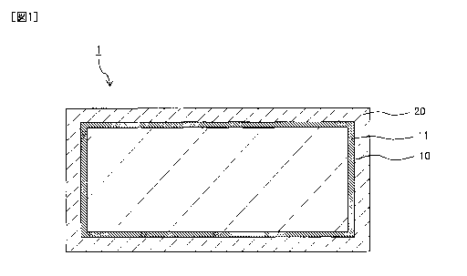
[0015]
FIG 1 is a cross-sectional view of a metal-plated stainless material according
to first
and second embodiments of the present invention.
FIG 2 is a set of views for explaining each step for producing the metal-
plated
stainless material in the first embodiment of the present invention.
FIG. 3 is a set of views for explaining each step for producing the metal-
plated
stainless material in the second embodiment of the present invention.
FIG. 4 is a view for explaining a method of measuring the contact resistance
of a
metal-plated stainless material 1 obtained in examples and comparative
examples.
[Mode(s) for Carrying out the Invention]
[0016]
Hereinafter, methods for producing a metal-plated stainless material 1
according to
embodiments of the present invention will be described.
[0017]
First Embodiment
The metal-plated stainless material 1 of a first embodiment is formed through
first
performing, as pretreatment, an acid treatment step of treating a stainless
steel material with an
acidic solution and an etching step of treating the stainless steel material
after the acid
treatment step with an etching treatment agent and then performing a
modification step of
5
CA 02969897 2017-06-06
modifying the surface of the stainless 'steel thaterial into a state suitable
for a metal plating
process and a metal plating step of forming a metal plating layer on the
stainless steel material.
Thus, the metal-plated stainless material 1 is configured such that, as
illustrated in FIG. 1, a
metal plating layer 20 is formed on an oxide film 11 that covers a stainless
steel material 10.
[0018]
<Acid Treatment Step>
In the first embodiment, the stainless steel sheet 10 to be a substrate of the
gold plate
coated stainless material 1 according to the present embodiment is prepared.
The stainless
steel sheet 10 is not particularly limited. Examples of the stainless steel
sheet 10 include
those made of stainless steel material, such as SUS316L, SUS316 and SUS304.
Various
types of stainless steel sheets may be mentioned, such as martensite-based,
ferrite-based and
austenite-based ones, among which austenite-based stainless steel sheets may
be preferred.
The shape and form of the stainless steel sheet 10 are not particularly
limited, and may be
appropriately selected depending on the use. For example, the stainless steel
sheet 10 may be
used after being worked into a necessary shape or form depending on its use,
such as a
conductive metal component worked into a linear form or a plate or sheet-like
form, a
conductive member obtained by working a plate or sheet into an irregular form,
and an
electronic device component worked into a spring-like or tubular form. The
length (or width)
and thickness (such as diameter) and sheet thickness (or plate thickness) of
the stainless steel
sheet 10 is also not particularly limited, and may be appropriately selected
depending on the
use.
[0019]
In the first embodiment, for the stainless steel material 10 thus prepared,
the acid
treatment step for treatment with an acidic solution is performed in control
of a predetermined
condition. In the first embodiment, the acid treatment step is performed to
allow the oxide
film 11, which includes a passivation film existing on the surface of the
stainless steel material
10 before the treatment with the acidic solution, to have a lower density.
Examples of the
method of forming the oxide film 11 having such a low density include a method
of treating
the stainless steel material 10 with the acidic solution to remove specific
components from the
passivation film, which exists on the surface of the stainless steel material
10 before the
treatment with the acidic solution, thereby to form the above oxide film 11.
Examples of
such specific components include, but are not limited to, iron oxide (such as
FeO and Fe203) in
the passivation film. Another example of the method of forming the above oxide
film 11
6
CA 02969897 2017-06-06
having a low density may be a method' of treating the stainless steel material
10 with the acidic
solution to remove at least a part of the passivation film, which exists on
the surface of the
stainless steel material 10 before the treatment with the acidic solution, so
that the above oxide
film 11 is formed as a new oxide film on the surface of the stainless steel
material 10.
In the first embodiment, when such an oxide film 11 is formed, as illustrated
in FIG. 2,
a thicker oxide film 11 than the oxide film 11, which includes the passivation
film existing
before the treatment with the acidic solution, may be formed. In this case, as
a result, most of
the oxide film on the surface of the stainless steel material 10 will grow.
FIG. 2 is a set of
views illustrating an example of appearances in which the metal-plated
stainless material 1 is
formed through the acid treatment step of treating an untreated stainless
steel material 10 with
the acidic solution, the etching step, the modification step for modification
into a state suitable
for a metal plating process, and the metal plating step. FIG. 2 also
illustrates graphs
representing variation in atomic concentrations (at%) of oxygen (0) and iron
(Fe) when
measurement is performed using a scanning-type Auger electron spectroscopy
analyzer (AES)
for the stainless steel material 10 after the acid treatment step for
treatment with the acidic
solution, the stainless steel material 10 after the etching step, and the
stainless steel material 10
after the modification step for modification into a state suitable for a metal
plating process.
In FIG 2, each vertical axis represents the atomic concentration of oxygen (0)
or iron (Fe)
while each horizontal axis represents the depth when measured from the surface
of the
stainless steel material 10 using the scanning-type Auger electron
spectroscopy analyzer
(AES).
[0020]
In the first embodiment, the treatment is performed in the above manner to
bring the
prepared stainless steel material 10 (denoted by "Untreated" in FIG 2) into
contact with the
acidic solution and the oxide film 11 can thereby be formed at the surface, as
illustrated in FIG
2. That is, with reference to the graphs obtained in the example of FIG 2
through the
measurement using the scanning-type Auger electron spectroscopy analyzer
(AES), the
thickness of the oxide film 11 increases from 4.6 nm in the untreated state to
19 nm after the
step of treatment with the acidic solution, provided that the thickness of the
oxide film 11 is
represented by the depth at a position in which the atomic concentration of
oxygen (0) falls
below the atomic concentration of iron (Fe).
[0021]
In the first embodiment, as described above, the oxide film 11 is formed using
the
acidic solution and the thickness of the oxide film 11 can thereby be uniform.
This will be
7
CA 02969897 2017-06-06
more specifically described. As illustrated i'n FIG. 2, in the untreated
stainless steel material
10, the thickness of the oxide film 11 including the passivation film is
nonuniform and,
therefore, parts with a thinner passivation film are further readily oxidized
while parts with a
thicker passivation film are less likely to be oxidized. In contrast, when the
surface of the
stainless steel material 10 is purposely oxidized to form the above-described
oxide film 11
using the acidic solution, the growth of the oxide film 11 to be formed at the
parts of the
stainless steel material 10 in which the oxidization is easy (parts with a
thinner passivation
film) progresses while the growth of the oxide film 11 to be formed at the
parts in which the
oxidization is difficult (parts with a thicker passivation film) is
suppressed. It is considered
that, as a result, the entire surface of the stainless steel material 10 is
evenly oxidized and the
oxide film 11 on the stainless steel material 10 can have a uniform thickness.
[0022]
In the first embodiment, the oxide film 11 formed by the acid treatment step
for
treatment with the acidic solution has properties that it can be relatively
easily removed using
an etching agent in the etching step which will be described later. This
appears to be because
the oxide film 11 formed by the acid treatment step for treatment with the
acidic solution has a
low density to such an extent that the oxide film 11 can be released using
adhesive tape. In
the first embodiment, such an acid treatment step for treatment with the
acidic solution and the
etching step are performed, and the thickness of the oxide film 11 on the
surface of the
stainless steel material 10 can thereby be purposely uniform. Thus, according
to the first
embodiment, a metal plating layer 20 can be successfully formed on the
obtained stainless
steel material covered with the oxide layer and it is possible to produce a
metal-plated stainless
material 1 that is excellent in the corrosion resistance, electrical
conductivity, smoothness, and
the like which are required for the metal plating layer 20.
[0023]
The acidic solution used in the acid treatment step for treatment with the
acidic
solution is not particularly limited, provided that it can reduce the density
to such an extent that
the oxide film 11 can be released using adhesive tape. It is preferred to use
any one of
hydrochloric acid, ammonium hydrogen fluoride, sulfuric acid, and nitric acid
or a mixture
thereof, among which hydrochloric acid is particularly preferred.
[0024]
In the acid treatment step for treatment with the acidic solution, aqueous
solution of
the above acidic solution is brought into contact with the stainless steel
material 10 and the
surface of the stainless steel material 10 can thereby be oxidized. The
concentration of the
8
CA 02969897 2017-06-06
acidic solution in the aqueous solution is preferably 1 to 99 wt% and may be
adjusted to a
concentration suitable for use in accordance with the type of the acidic
solution. In particular,
when the treatment is performed using hydrochloric acid, the concentration is
preferably 10 to
35 wt% and more preferably 15 to 25 wt%. The concentration of the acidic
solution within
the above range allows the surface of the stainless steel material 10 to be
appropriately
oxidized.
[0025]
It suffices that the method of bringing the stainless steel material 10 into
contact with
the acidic solution is a method with which the oxide film 11 can be
appropriately formed to
have a uniform thickness as much as possible. Examples of such a method
include a method
of immersing the stainless steel material 10 in the aqueous solution of the
acidic solution and a
method of spraying the aqueous solution of the acidic solution to the
stainless steel material
10.
[0026]
When the stainless steel material 10 is immersed in the aqueous solution of
the acidic
solution, the temperature of the aqueous solution is preferably 40 C to 80 C
and more
preferably 50 C to 65 C. The time for immersing the stainless steel material
10 in the
aqueous solution of the acidic solution is preferably 5 to 120 seconds and
more preferably 10
to 60 seconds.
[0027]
<Etching Step>
Subsequently, treatment of the etching step is performed to reduce the
thickness of the
oxide film 11, as illustrated in FIG. 2, through bringing the etching agent
into contact with the
stainless steel material 10 on which the oxide film 11 is formed by the acid
treatment step.
[0028]
In the first embodiment, the treatment is performed in the above manner to
bring the
stainless steel material 10 after the acid treatment step into contact with
the etching agent in
control of a predetermined condition, and the thickness of the oxide film 11
at the surface can
thereby be reduced, as illustrated in FIG. 2. That is, with reference to the
graphs obtained in
the example illustrated in FIG. 2 through the measurement using the scanning-
type Auger
electron spectroscopy analyzer (AES), the thickness of the oxide film 11
decreases from 19 nm
after the acid treatment step to 9.2 nm after the etching step, provided that
the thickness of the
oxide film 11 is represented by the depth at a position in which the atomic
concentration of
oxygen (0) falls below the atomic concentration of iron (Fe).
9
CA 02969897 2017-06-06
[0029]
The etching agent used in the etching step is not particularly limited, but it
is preferred
to use any one of nitric acid and sulfuric acid or a mixture thereof, among
which nitric acid is
particularly preferred.
[0030]
In the etching step, aqueous solution of the above etching agent is brought
into contact
with the stainless steel material 10, and a part of the oxide film 11 on the
surface of the
stainless steel material 10 can thereby be removed. The concentration of the
etching agent in
the aqueous solution is preferably 5 to 30 wt% and more preferably 10 to 25
wt%. When the
concentration of the etching agent is within the above range, the thickness of
the oxide film 11
of the stainless steel material 10 can be appropriately reduced and the
thickness of the oxide
film 11 remaining on the stainless steel material 10 can be uniform.
[0031]
It suffices that the method of bringing the stainless steel material 10 into
contact with
the etching agent is a method with which the thickness of the oxide film 11
can be
appropriately reduced while remaining uniform as much as possible. Examples of
such a
method include a method of immersing the stainless steel material 10 in the
aqueous solution
of the etching agent and a method of spraying the aqueous solution of the
etching agent to the
stainless steel material 10.
[0032]
When the stainless steel material 10 is immersed in the aqueous solution of
the
etching agent, the temperature of the aqueous solution is preferably 20 C to
60 C and more
preferably 25 C to 40 C. The time for immersing the stainless steel material
10 in the
aqueous solution of the etching agent is preferably 1 to 30 seconds and more
preferably 2 to 15
seconds.
[0033]
In the first embodiment, when a part of the oxide film 11 is removed in the
etching
step, it is preferred not to expose the base iron of the stainless steel
material 10 (a base portion
of the stainless steel material 10 that is not oxidized to be the oxide film
11). This will be
more specifically described. If the base iron of the stainless steel material
10 is exposed, the
exposed portion will come into contact with oxygen in the air and/or oxygen in
water to
naturally generate a new oxide film 11. Such a naturally-generated oxide film
11 is liable to
have a nonuniform thickness. In the first embodiment, therefore, the thickness
of the oxide
film 11 is reduced in the etching step to such an extent that the base iron of
the stainless steel
CA 02969897 2017-06-06
material 10 is not exposed, thereby to prev&A the new oxide film 11 from being
naturally
generated on the stainless steel material 10, and the thickness of the oxide
film 11 can remain
uniform.
[0034]
<Modification Step>
Then, for the stainless steel material 10 having the oxide film 11 of which
the
thickness is reduced in the etching step, treatment of the modification step
is performed to
modify the oxide film 11 at the surface into a state suitable for a metal
plating process. In the
first embodiment, the treatment of the modification step is performed and the
stainless steel
material 10 is thereby obtained which is covered with the oxide film 11, as
illustrated in FIGS.
1 and 2.
[0035]
Examples of the state suitable for a metal plating process include a state in
which the
Cr/0 value (molar ratio of Cr/O) and Cr/Fe value (molar ratio of Cr/Fe) as
measured by the
scanning-type Auger electron spectroscopy analysis for the surface of the
oxide film 11 are
adjusted within the following ranges. That is, the Cr/0 value is preferably
within a range of
0.05 to 0.2 and more preferably within a range of 0.05 to 0.15. The Cr/Fe
value is preferably
within a range of 0.5 to 0.8 and more preferably within a range of 0.5 to 0.7.
[0036]
In the first embodiment, when the Cr/0 value and Cr/Fe value as measured by
Auger
electron spectroscopy analysis are controlled within the above ranges on the
surface of the
oxide film 11 of the stainless steel material 10, the metal plating layer 20
formed on the oxide
film 11 can have an improved coverage (i.e., a ratio of an area covered with
the metal plating
layer 20 to the surface of the oxide film 11 on which the metal plating layer
20 is formed) and
can be excellent in the interfacial adhesion property and the corrosion
resistance.
[0037]
In the first embodiment, the Cr/0 value and Cr/Fe value can be measured by
Auger
electron spectroscopy analysis, for example, using the following method.
First, a
scanning-type Auger electron spectroscopy analyzer (AES) is used to measure
the surface of
the oxide film 11, and the atomic percentages of Cr, 0, and Fe at the surface
of the oxide film
11 are calculated. Five locations at the surface of the oxide film 11 are
measured using the
scanning-type Auger electron spectroscopy analyzer, and the obtained results
may be averaged
thereby to calculate the Cr/0 value (at% of Cr/at% of 0) and the Cr/Fe value
(at% of Cr/at% of
Fe). In the first embodiment, among the obtained peaks by the measurement
using the
11
CA 02969897 2017-06-06
scanning-type Auger electron spectrokopy analyzer, a peak given within 510 to
535 eV
represents the peak of Cr, a peak given within 485 to 520 eV represents the
peak of 0, and a
peak given within 570 to 600 eV represents the peak of Fe. The atomic
percentages of Cr, 0,
and Fe are to be measured when the sum of Cr, 0, and Fe is 100 at%.
[0038]
In the modification step for modification into a state suitable for the metal
plating
process of the first embodiment, examples of the method of putting the Cr/0
value and Cr/Fe
value as measured by the scanning-type Auger electron spectroscopy analysis
into the above
ranges include a method of immersing the stainless steel material 10 after the
etching step in a
sulfuric acid aqueous solution.
[0039]
When the stainless steel material 10 is immersed in a sulfuric acid aqueous
solution in
the modification step for modification into a state suitable for the metal
plating process, the
sulfuric acid concentration in the sulfuric acid aqueous solution is
preferably 20 to 25 vol%.
The temperature when immersing the stainless steel material 10 is preferably
50 C to 70 C and
more preferably 60 C to 70 C. The time for immersing the stainless steel
material 10 in the
sulfuric acid aqueous solution is preferably 3 to 600 seconds and more
preferably 5 to 300
seconds.
[0040]
According to the first embodiment, when the method is used in which the
stainless
steel material 10 is immersed in a sulfuric acid aqueous solution in the
modification step for
modification into a state suitable for the metal plating process, the
conditions of the sulfuric
acid concentration, temperature, and immersion time are set within the above
ranges.
Through this setting, a part of the oxide film 11 on the surface of the
stainless steel material 10
is removed and the stainless steel material 10 can have a surface of which the
Cr/0 value and
Cr/Fe value as measured by the Auger electron spectroscopy analysis are
controlled within the
above-described ranges.
[0041]
In the first embodiment, the stainless steel material 10 having the oxide film
11 of
which the thickness has been reduced in the etching step is subjected to the
above-described
modification step for modification into a state suitable for the metal plating
process thereby to
have a further reduced thickness of the oxide film 11 in general. For example,
with reference
to the graphs obtained in the example illustrated in FIG 2 through the
measurement using the
scanning-type Auger electron spectroscopy analyzer (AES), the thickness of the
oxide film 11
12
CA 02969897 2017-06-06
decreases from 9.2 nm after the etChing step to 6.7 nm after the modification
step for
modification into a state suitable for the metal plating process, provided
that the thickness of
the oxide film 11 is represented by the depth at a position in which the
atomic concentration of
oxygen (0) falls below the atomic concentration of iron (Fe).
[0042]
<Metal Plating Step>
Then, for the stainless steel material 10 which is modified by the
modification step for
modification into a state suitable for the metal plating process, a process of
the metal plating
step is performed to form a metal plating layer 20 at the surface.
[0043]
The metal which constitutes the metal plating layer 20 may be, but is not
limited to,
any one of gold (Au), silver (Ag), palladium (Pd), platinum (Pt), rhodium
(Rh), ruthenium (Ru),
copper (Cu), tin (Sn), chromium (Cr), nickel (Ni), cobalt (Co), iron (Fe),
phosphorus (P), and
boron (B) or an alloy that contains two or more of the above metals. Among
these, Au, Ag,
Pd, or Pt may be particularly preferred. The method of plating for forming the
metal plating
layer 20 is not particularly limited, but it is preferred to form the metal
plating layer 20 by
electroless plating using a plating bath that contains a salt of Au, Ag, Pd,
Pt, Rh, Ru, Cu, Sn, Cr,
Ni, Co, Fe, P, B, and the like.
[0044]
Au, Ag, Pd, Pt, Rh, Ru, Cu, Sn, Cr, and Ni as mentioned herein have common
properties that they are noble metals having a high normal electrode potential
and the contact
resistance is low. When any of the above metals is used as the metal which
constitutes the
metal plating layer 20, therefore, the obtained metal-plated stainless
material 1 is excellent in
the properties, such as plating property, interfacial adhesion property,
corrosion resistance, and
electrical conductivity, of the metal plating layer 20.
[0045]
The coverage of the metal plating layer 20, that is, the ratio of an area
covered by the
metal plating layer 20 to the surface of the oxide film 11 on which the metal
plating layer 20 is
formed, is preferably 95% or more. When the coverage of the metal plating
layer 20 is 95%
or more, pinholes in the metal plating layer 20 can be reduced thereby to
prevent the
delamination of the metal plating layer 20 triggered from such pinholes and to
further improve
the corrosion resistance and electrical conductivity of the obtained metal-
plated stainless
material 1.
[0046]
13
CA 02969897 2017-06-06
When gold is used as a primary metal that constitutes the metal plating layer
20, the
thickness of the metal plating layer 20 to be formed is preferably 2 to 20 nm
and more
preferably 2 to 10 nm. If the thickness of the metal plating layer 20 formed
primarily of gold
is unduly thin, the metal plating layer 20 will not be uniformly formed on the
oxide film 11 of
the stainless steel material 10, and the corrosion resistance and electrical
conductivity of the
metal-plated stainless material 1 may possibly deteriorate. On the other hand,
an unduly thick
thickness of the metal plating layer 20 formed primarily of gold may lead to
disadvantages in
cost.
[0047]
When silver is used as a primary metal that constitutes the metal plating
layer 20, the
thickness of the metal plating layer 20 to be formed is preferably 10 to 200
nm and more
preferably 20 to 100 nm. If the thickness of the metal plating layer 20 formed
primarily of
silver is unduly thin, the metal plating layer 20 will not be uniformly formed
on the oxide film
11 of the stainless steel material 10, and the corrosion resistance and
electrical conductivity of
the metal-plated stainless material 1 may possibly deteriorate. On the other
hand, an unduly
thick thickness of the metal plating layer 20 formed primarily of silver may
lead to
disadvantages in cost.
[0048]
When a metal other than gold and silver is used as a primary metal that
constitutes the
metal plating layer 20, the thickness of the metal plating layer 20 to be
formed is preferably 2
to 20 nm and more preferably 2 to 10 nm. If the thickness of the metal plating
layer 20
formed of such a metal is unduly thin, the metal plating layer 20 will not be
uniformly formed
on the oxide film 11 of the stainless steel material 10, and the corrosion
resistance and
electrical conductivity of the metal-plated stainless material 1 may possibly
deteriorate. On
the other hand, an unduly thick thickness of the metal plating layer 20 formed
of such a metal
may lead to disadvantages in cost.
[0049]
As the above, the metal-plated stainless material 1 can be obtained through
the metal
plating step in which the metal plating process is performed for the stainless
steel material 10
to form the metal plating layer 20 on the oxide film 11.
[0050]
According to the first embodiment, the acid treatment step for treatment with
the
acidic solution and the etching step as described above allow the oxide film
11 to have a
uniform thickness even when the stainless steel material 10 prepared as a
substrate has a
14
CA 02969897 2017-06-06
variation in the thickness of a naturally:generaied oxide film 11 on the
surface (i.e., a variation
in the thickness of the oxide film 11 based on the individual difference of
the stainless steel
material and/or a variation in the thickness of the oxide film 11 on the same
surface of a
stainless steel material). Specifically, even when the thickness of the oxide
film 11 varies in
the untreated stainless steel material 10, the oxide film 11 of the stainless
steel material 10 can
be adjusted to have a uniform thickness through the formation in the acid
treatment step for
treatment with the acidic solution and the subsequent thickness reduction in
the etching step,
regardless of the individual difference and variety of the thickness of the
oxide film 11
generated on the surface of the stainless steel material 10.
[0051]
Moreover, according to the first embodiment, for the oxide film 11 thus having
a
uniform thickness, the above-described modification step for modification into
a state suitable
for a metal plating process is performed and the oxide film 11 can thereby be
brought into the
state suitable for a metal plating process. Thereafter, in the metal plating
step, the metal
plating layer 20 can be formed to have a thin and uniform thickness.
[0052]
Thus, according to the first embodiment, the oxide film 11 suitable for a
metal plating
process can be formed to have a uniform thickness regardless of the variation
in the oxide film
11 generated on the surface of the stainless steel material 10 and the metal
plating layer 20 can
be formed on such an oxide film 11 so as to have a thin and uniform thickness.
As a result,
according to the first embodiment, it is possible to produce a metal-plated
stainless material 1
that is excellent in the interfacial adhesion property and corrosion
resistance of the metal
plating layer 20.
[0053]
The metal-plated stainless material 1 of the first embodiment can be used as
an
electrical contact material such as used for connectors, switches, or printed
wiring boards, as
described above, but may also be used as a separator for fuel cells. Such a
separator for fuel
cells is used as a member of a fuel cell that constitutes a fuel cell stack,
and has a function to
supply an electrode with fuel gas or air through gas flow channels and a
function to collect
electrons generated at the electrode. When the metal-plated stainless material
1 is used as a
separator for fuel cells, it is preferred to prepare a stainless steel
material 10 of which the
surface is preliminarily formed with irregularities (gas flow channels) that
function as flow
channels for fuel gas or air and perform each treatment or process of the acid
treatment step for
treatment with the acidic solution, the etching step, the modification step
for modification into
CA 02969897 2017-06-06
a state suitable for a metal plating process, arid the metal plating step, as
described above, for
the stainless steel material 10. The method of forming such gas flow channels
is not
particularly limited, but a method of forming the gas flow channels by press
working may be
mentioned, for example.
[0054]
In general, a separator for fuel cells is exposed to an environment of high
temperature
and acidic atmosphere in the fuel cells. Accordingly, when a stainless steel
material formed
with a metal plating layer at the surface is used as a separator for fuel
cells, if the coverage of
the metal plating layer at the surface is low, corrosion of the stainless
steel material as a
substrate will progress rapidly. This may result in a problem in that the
electrical resistance
value increases due to the corrosion product generated on the surface of the
stainless steel
material to deteriorate the function as a separator for fuel cells, that is,
the function of
collecting electrons generated at the electrode.
[0055]
In contrast, the metal-plated stainless material 1 according to the first
embodiment is
formed with the metal plating layer 20 which is excellent in the coverage and
interfacial
adhesion property as described above, and can be suitably used as such a
separator for fuel
cells.
[0056]
Second Embodiment
The metal-plated stainless material 1 of a second embodiment is formed through
first
performing, as pretreatment, a film thickness reduction step of treating a
stainless steel
material 10 with an etching treatment agent to reduce the thickness of an
oxide film 11
including a passivation film and a film growth step of growing the oxide film
11 using an
oxidation treatment agent and then performing a modification step of modifying
the oxide film
11 and a metal plating step of forming a metal plating layer on the stainless
steel material.
Thus, the metal-plated stainless material 1 is configured such that, as
illustrated in FIG. 1, the
metal plating layer 20 is formed on the oxide film 11 which covers the
stainless steel material
10.
[0057]
<Film Thickness Reduction Step>
In the second embodiment, first, the stainless steel material 10 as a
substrate of the
metal-plated stainless material 1 is prepared. The substrate to be used may be
the same as
that in the above-described first embodiment.
16
CA 02969897,2017-06-06
[0058]
In the second embodiment, for the prepared stainless steel material 10,
treatment of
the film thickness reduction step is performed in control of a predetermined
condition to
reduce the thickness of the oxide film 11, which includes a naturally-
generated passivation
film on the surface, using an etching agent. Specifically, the stainless steel
material 10 is
brought into contact with the etching agent to remove a part of the oxide film
11 on the surface
of the stainless steel material 10 and, as illustrated in FIG 3, the thickness
of the oxide film 11
is reduced. FIG. 3 is a set of views illustrating an example of appearances in
which the
metal-plated stainless material 1 is formed from the untreated stainless steel
material 10
through the film thickness reduction step, film growth step, modification
step, and metal
plating step. FIG. 3 also illustrates graphs representing variation in atomic
concentrations
(at%) of oxygen (0) and iron (Fe) when measurement is performed using a
scanning-type
Auger electron spectroscopy analyzer (AES) for the stainless steel material 10
after the film
thickness reduction step, the stainless steel material 10 after the film
growth step, and the
stainless steel material 10 after the modification step. In FIG 3, each
vertical axis represents
the atomic concentration of oxygen (0) or iron (Fe) while each horizontal axis
represents the
depth when measured from the surface of the stainless steel material 10 using
the
scanning-type Auger electron spectroscopy analyzer (AES).
[0059]
In the second embodiment, the treatment is performed in the above manner to
bring
the prepared stainless steel material 10 (denoted by "Untreated" in FIG. 3)
into contact with the
etching agent and the thickness of the oxide film 11 at the surface can
thereby be reduced, as
illustrated in FIG 3. That is, with reference to the graphs obtained in the
example of FIG. 3
through the measurement using the scanning-type Auger electron spectroscopy
analyzer (AES),
the thickness of the oxide film 11 decreases from 4.6 nm in the untreated
state to 4.0 nm after
the film thickness reduction step, provided that the thickness of the oxide
film 11 is
represented by the depth at a position in which the atomic concentration of
oxygen (0) falls
below the atomic concentration of iron (Fe). In the second embodiment, the
oxide film 11 of
which the thickness is reduced through the film thickness reduction step has a
totally-reduced
thickness, as illustrated in FIG 3.
[0060]
The etching agent used in the film thickness reduction step is not
particularly limited,
provided that it can reduce the thickness of the oxide film 11. It is
preferred to use any one of
ammonium hydrogen fluoride, sulfuric acid, nitric acid, and hydrochloric acid
or a mixture
17
CA 02969897 2017-06-06
thereof, among which ammonium hydrogen fluoride or a mixed acid of
hydrochloric acid and
nitric acid is particularly preferred.
[0061]
In the film thickness reduction step, aqueous solution of the above etching
agent is
brought into contact with the stainless steel material 10, and a part of the
oxide film 11 on the
surface of the stainless steel material 10 can thereby be removed. The
concentration of the
etching agent in the aqueous solution is preferably 1 to 99 wt% and may be
adjusted to a
concentration suitable for use in accordance with the type of the etching
agent. In particular,
when the treatment is performed using ammonium hydrogen fluoride, the
concentration is
preferably 1 to 15 wt% and more preferably 3 to 5 wt%. The concentration of
the etching
agent within the above range allows the thickness of the oxide film 11 of the
stainless steel
material 10 to be appropriately reduced.
[0062]
It suffices that the method of bringing the stainless steel material 10 into
contact with
the etching agent is a method with which the thickness of the oxide film 11
can be
appropriately reduced with a uniform thickness as much as possible. Examples
of such a
method include a method of immersing the stainless steel material 10 in the
aqueous solution
of the etching agent and a method of spraying the aqueous solution of the
etching agent to the
stainless steel material 10.
[0063]
When the stainless steel material 10 is immersed in the aqueous solution of
the
etching agent, the temperature of the aqueous solution is preferably 20 C to
60 C and more
preferably 25 C to 50 C. The time for immersing the stainless steel material
10 in the
aqueous solution of the etching agent is preferably 5 to 600 seconds and more
preferably 10 to
120 seconds.
[0064]
In the second embodiment, when a part of the oxide film 11 is removed in the
film
thickness reduction step, it is preferred not to expose the base iron of the
stainless steel
material 10 (a base portion of the stainless steel material 10 that is not
oxidized to be the oxide
film 11). This will be more specifically described. If the base iron of the
stainless steel
material 10 is exposed, the exposed portion will come into contact with oxygen
in the air
and/or oxygen in water to naturally generate a new oxide film 11. Such a
naturally-generated
oxide film 11 is liable to have a nonuniform thickness. In the second
embodiment, therefore,
the thickness of the oxide film 11 is reduced in the film thickness reduction
step to such an
18
CA 02969897 2017-06-06
extent that the base iron of the stainlesg steel Material 10 is not exposed,
thereby to prevent the
new oxide film 11 from being naturally generated on the stainless steel
material 10.
[0065]
<Film Growth Step>
Subsequently, treatment of the film growth step is performed to grow the oxide
film
11, as illustrated in FIG 3, through bringing an oxidation treatment agent
into contact with the
stainless steel material 10 on which the thickness of the oxide film 11 is
reduced by the film
thickness reduction step.
[0066]
In the second embodiment, the treatment is performed in the above manner to
bring
the stainless steel material 10 after the film thickness reduction step into
contact with the
oxidation treatment agent in control of a predetermined condition, and the
oxide film 11 can
thereby grow, as illustrated in FIG. 3. That is, with reference to the graphs
obtained in the
example illustrated in FIG. 3 through the measurement using the scanning-type
Auger electron
spectroscopy analyzer (AES), the thickness of the oxide film 11 increases from
4.0 nm after
the film thickness reduction step to 6.2 nm after the film growth step,
provided that the
thickness of the oxide film 11 is represented by the depth at a position in
which the atomic
concentration of oxygen (0) falls below the atomic concentration of iron (Fe).
[0067]
In the second embodiment, as described above, the oxide film 11 can be grown
using
the oxidation treatment agent thereby to have an increased and uniform
thickness. This will
be more specifically described. As illustrated in FIG 3, in the stainless
steel material 10 in
which the thickness of the oxide film 11 of the untreated stainless steel
material 10 is totally
reduced (stainless steel material 10 after the film thickness reduction step),
the thickness of the
oxide film 11 is nonuniform and, therefore, parts with a thinner oxide film 11
are further
readily oxidized while parts with a thicker oxide film 11 are less likely to
be oxidized. In
contrast, when the surface of the stainless steel material 10 is purposely
oxidized using the
oxidation treatment agent, the growth of the oxide film 11 to be formed at the
parts of the
stainless steel material 10 in which the oxidization is easy (parts with a
thinner oxide film 11)
progresses while the growth of the oxide film 11 to be formed at the parts in
which the
oxidization is difficult (parts with a thicker oxide film 11) is suppressed.
As a result, the
entire surface of the stainless steel material 10 is evenly oxidized and the
oxide film 11 on the
stainless steel material 10 can have a uniform thickness.
[0068]
19
CA 02969897 2017-06-06
In the second embodiment, the' above2described film thickness reduction step
and film
growth step are performed, and the thickness of the oxide film 11 on the
surface of the
stainless steel material 10 can thereby be purposely uniform. Thus, according
to the second
embodiment, a metal plating layer 20 can be successfully formed on the
obtained stainless
steel material covered with the oxide layer and it is possible to produce a
metal-plated stainless
material 1 that is excellent in the interfacial adhesion property and
corrosion resistance of the
metal plating layer 20.
[0069]
The oxidation treatment agent used in the film growth step is not particularly
limited,
provided that the oxide film 11 can be appropriately grown, but it is
preferred to use any one of
nitric acid and sulfuric acid or a mixture thereof, among which nitric acid is
particularly
preferred.
[0070]
In the film growth step, aqueous solution of the above oxidation treatment
agent is
brought into contact with the stainless steel material 10, and the surface of
the stainless steel
material 10 can thereby be oxidized. The concentration of the oxidation
treatment agent in
the aqueous solution is preferably 5 to 25 wt% and more preferably 15 to 20
wt%. When the
concentration of the oxidation treatment agent is within the above range, the
surface of the
stainless steel material 10 can be appropriately oxidized.
[0071]
It suffices that the method of bringing the stainless steel material 10 into
contact with
the oxidation treatment agent is a method with which the oxide film 11 can
grow with its
uniform thickness as much as possible. Examples of such a method include a
method of
immersing the stainless steel material 10 in the aqueous solution of the
oxidation treatment
agent and a method of spraying the aqueous solution of the oxidation treatment
agent to the
stainless steel material 10.
[0072]
When the stainless steel material 10 is immersed in the aqueous solution of
the
oxidation treatment agent, the temperature of the aqueous solution is
preferably 20 C to 60 C
and more preferably 25 C to 40 C. The time for immersing the stainless steel
material 10 in
the aqueous solution of the oxidation treatment agent is preferably 1 to 30
seconds and more
preferably 2 to 15 seconds.
[0073]
<Modification Step>
CA 02969897 2017-06-06
Then, for the stainless steel material 10 of which the oxide film 11 grows in
the film
growth step, treatment of the modification step is performed to modify the
oxide film 11 at the
surface into a state suitable for a metal plating process, as in the first
embodiment. In the
second embodiment, the treatment of the modification step is performed and the
stainless steel
material 10 is thereby obtained which is covered with the oxide film 11, as
illustrated in FIGS.
1 and 3.
[0074]
Examples of the state suitable for a metal plating process include a state in
which the
Cr/0 value (molar ratio of Cr/O) and Cr/Fe value (molar ratio of Cr/Fe) as
measured by the
scanning-type Auger electron spectroscopy analysis for the surface of the
oxide film 11 are
adjusted within the following ranges. That is, the Cr/0 value is preferably
within a range of
0.05 to 0.2 and more preferably within a range of 0.05 to 0.15. The Cr/Fe
value is preferably
within a range of 0.5 to 0.8 and more preferably within a range of 0.5 to 0.7.
[0075]
In the second embodiment, when the Cr/0 value and Cr/Fe value as measured by
Auger electron spectroscopy analysis are controlled within the above ranges on
the surface of
the oxide film 11 of the stainless steel material 10, the metal plating layer
20 formed on the
oxide film 11 can have an improved coverage (i.e., a ratio of an area covered
with the metal
plating layer 20 to the surface of the oxide film 11 on which the metal
plating layer 20 is
formed) and can be excellent in the interfacial adhesion property and the
corrosion resistance.
[0076]
In the second embodiment, the Cr/0 value and Cr/Fe value can be measured by
Auger
electron spectroscopy analysis, for example, using the following method.
First, a
scanning-type Auger electron spectroscopy analyzer (AES) is used to measure
the surface of
the oxide film 11, and the atomic percentages of Cr, 0, and Fe at the surface
of the oxide film
11 are calculated. Five locations at the surface of the oxide film 11 are
measured using the
scanning-type Auger electron spectroscopy analyzer, and the obtained results
may be averaged
thereby to calculate the Cr/0 value (at% of Cr/at% of 0) and the Cr/Fe value
(at% of Cr/at% of
Fe). In the second embodiment, among the obtained peaks by the measurement
using the
scanning-type Auger electron spectroscopy analyzer, a peak given within 510 to
535 eV
represents the peak of Cr, a peak given within 485 to 520 eV represents the
peak of 0, and a
peak given within 570 to 600 eV represents the peak of Fe. The atomic
percentages of Cr, 0,
and Fe are to be measured when the sum of Cr, 0, and Fe is 100 at%.
[0077]
21
CA 02969897 2017-06-06
In the modification step of the 'second 'embodiment, examples of the method of
putting
the Cr/0 value and Cr/Fe value as measured by the scanning-type Auger electron
spectroscopy
analysis into the above ranges include a method of immersing the stainless
steel material 10
after the film growth step in a sulfuric acid aqueous solution.
[0078]
When the stainless steel material 10 is immersed in a sulfuric acid aqueous
solution in
the modification step, the sulfuric acid concentration in the sulfuric acid
aqueous solution is
preferably 20 to 25 vol%. The temperature when immersing the stainless steel
material 10 is
preferably 50 C to 70 C and more preferably 60 C to 70 C. The time for
immersing the
stainless steel material 10 in the sulfuric acid aqueous solution is
preferably 3 to 600 seconds
and more preferably 5 to 300 seconds.
[0079]
According to the second embodiment, when the method is used in which the
stainless
steel material 10 is immersed in a sulfuric acid aqueous solution in the
modification step, the
conditions of the sulfuric acid concentration, temperature, and immersion time
are set within
the above ranges. Through this setting, a part of the oxide film 11 on the
surface of the
stainless steel material 10 is removed and the stainless steel material 10 can
have a surface of
which the Cr/0 value and Cr/Fe value as measured by the Auger electron
spectroscopy
analysis are controlled within the above-described ranges.
[0080]
In the second embodiment, the stainless steel material 10 of which the oxide
film 11
has grown in the film growth step is subjected to the above-described
modification step
thereby to have a reduced thickness of the oxide film 11 in general. For
example, with
reference to the graphs obtained in the example illustrated in FIG 3 through
the measurement
using the scanning-type Auger electron spectroscopy analyzer (AES), the
thickness of the
oxide film 11 decreases from 6.2 nm after the film growth step to 2.7 nm after
the modification
step, provided that the thickness of the oxide film 11 is represented by the
depth at a position
in which the atomic concentration of oxygen (0) falls below the atomic
concentration of iron
(Fe).
[0081]
<Metal Plating Step>
Then, for the stainless steel material 10 which is modified by the
modification step, a
process of the metal plating step is performed to form a metal plating layer
20 at the surface, as
in the above-described first embodiment. The metal-plated stainless material 1
can thus be
22
CA 02969897 2017-06-06
obtained through the metal plating step in which the metal plating process is
performed for the
stainless steel material 10 to form the metal plating layer 20 on the oxide
film 11.
[0082]
According to the second embodiment, the film thickness reduction step and the
film
growth step allow the oxide film 11 to have a uniform thickness even when the
stainless steel
material 10 prepared as a substrate has a variation in the thickness of a
naturally-generated
oxide film 11 on the surface (i.e., a variation in the thickness of the oxide
film 11 based on the
individual difference of the stainless steel material and/or a variation in
the thickness of the
oxide film 11 on the same surface of a stainless steel material).
Specifically, even when the
thickness of the oxide film 11 varies in the untreated stainless steel
material 10, the oxide film
11 of the stainless steel material 10 can be adjusted to have a uniform
thickness through the
reduction of the thickness in the film thickness reduction step and the
subsequent increase of
the thickness in the film growth step, regardless of the individual difference
and variety of the
thickness of the oxide film 11 generated on the surface of the stainless steel
material 10.
[0083]
Moreover, according to the second embodiment, for the oxide film 11 thus
having a
uniform thickness, the above-described modification step is performed and the
oxide film 11
can thereby be brought into the state suitable for a metal plating process.
Thereafter, in the
metal plating step, the metal plating layer 20 can be formed to have a thin
and uniform
thickness.
[0084]
Thus, according to the second embodiment, the oxide film 11 suitable for a
metal
plating process can be formed to have a uniform thickness regardless of the
variation in the
oxide film 11 generated on the surface of the stainless steel material 10 and
the metal plating
layer 20 can be formed on such an oxide film 11 so as to have a thin and
uniform thickness.
As a result, according to the second embodiment, it is possible to produce a
metal-plated
stainless material 1 that is excellent in the interfacial adhesion property
and corrosion
resistance of the metal plating layer 20.
[0085]
The metal-plated stainless material 1 of the second embodiment can be used not
only
as an electrical contact material such as used for connectors, switches, or
printed wiring boards,
as in the above-described first embodiment, but also as a separator for fuel
cells. The
metal-plated stainless material 1 according to the second embodiment is formed
with the metal
plating layer 20 which is excellent in the coverage and interfacial adhesion
property as
23
CA 02969897 2017-06-06
described above, and can be suitably used as a Separator for fuel cells.
[Examples]
[0086]
Hereinafter, the present invention will be more specifically described with
reference to
examples, but the present invention is not limited to these examples.
Evaluation method for the metal-plated stainless material 1 obtained in each
of the
examples and comparative example is as follows.
[0087]
<Measurement of Contact Resistance Value>
For the metal-plated stainless material 1, measurement of the contact
resistance value
was performed using a measurement system as illustrated in FIG. 4. The
measurement system
illustrated in FIG. 4 is composed of two metal-plated stainless materials 1,
gold-plated copper
electrodes 2, a voltmeter 3, and an ammeter 4. Specifically, for the
measurement of the
contact resistance value, the metal-plated stainless materials 1 were first
worked into a size of
width of 20 mm, length of 20 mm, and thickness of 0.1 mm. Two of the metal-
plated
stainless materials 1 were overlapped each other and interposed between the
gold-plated
copper electrodes 2 from both sides to be fixed, and the measurement system
was thus
obtained as illustrated in FIG. 4. Then, the contact resistance value of the
test pieces was
measured using an ohm meter (Milli-Ohm HiTESTER 3540 available from HIOKI E.E.
CORPORATION) while applying a constant load to the gold-plated copper
electrodes 2.
[0088]
Example 1
First, a plate of SUS316L was prepared as the stainless steel material 10.
Then, the
prepared stainless steel material 10 was washed with water and degreased and
thereafter
treatment was performed such that the stainless steel material 10 was immersed
in a
hydrochloric acid aqueous solution of a hydrochloric acid concentration of 20
wt% under a
condition of a temperature of 60 C and an immersion time of 60 seconds
(treatment of the acid
treatment step for treatment with an acidic solution) thereby to form the
oxide film 11 on the
surface of the stainless steel material 10.
[0089]
Next, the stainless steel material 10 formed with the oxide film 11 was washed
with
water and thereafter treatment was performed such that the stainless steel
material 10 was
immersed in a nitric acid aqueous solution of a nitric acid concentration of
20 wt% under a
condition of a temperature of 30 C and an immersion time of 3 seconds
(treatment of the
24
CA 02969897 2017-06-06
etching step) thereby to reduce the thickness of the oxide film 11 on the
surface of the stainless
steel material 10.
=
[0090]
Subsequently, the stainless steel material 10 formed with the oxide film 11
having the
reduced thickness was washed with water and thereafter treatment was performed
such that the
stainless steel material 10 was immersed in a sulfuric acid aqueous solution
of a sulfuric acid
concentration of 25 vol% under a condition of a temperature of 70 C and an
immersion time of
5 seconds (treatment of the modification step for modification into a state
suitable for a metal
plating process) thereby to modify the oxide film 11 on the surface of the
stainless steel
material 10.
[0091]
Then, the stainless steel material 10 formed with the modified oxide film 11
was
washed with water and thereafter treatment of electroless plating was
performed under a
condition of 38 C, pH of 5.5, and 4 minutes using an electroless palladium
alloy plating bath
(treatment of the metal plating step) thereby to form the metal plating layer
20 of a thickness of
about 40 nm on the oxide film 11. The metal-plated stainless material 1 was
thus obtained.
[0092]
Subsequently, for the obtained metal-plated stainless material 1, the
measurement of
the contact resistance was performed in accordance with the above-described
method.
Furthermore, heat treatment was performed to maintain the metal-plated
stainless material 1
under an environment of a temperature of 250 C for 1 hour and the measurement
of the contact
resistance was performed again. Results are listed in Table 1.
[0093]
Example 2
First, SUS316L was prepared as the stainless steel material 10. Then, the
prepared
stainless steel material 10 was washed with water and degreased and thereafter
treatment was
performed such that the stainless steel material 10 was immersed in an
ammonium hydrogen
fluoride aqueous solution of an ammonium hydrogen fluoride concentration of 3
wt% under a
condition of a temperature of 30 C and an immersion time of 60 seconds
(treatment of the film
thickness reduction step) thereby to reduce the thickness of the oxide film 11
on the surface of
the stainless steel material 10.
[0094]
Next, the stainless steel material 10 formed with the oxide film 11 having the
reduced
thickness was washed with water and thereafter treatment was performed such
that the
CA 02969897 2017-06-06
stainless steel material 10 was immeised in a nitric acid aqueous solution of
a nitric acid
concentration of 20 wt% under a condition of a temperature of 30 C and an
immersion time of
3 seconds (treatment of the film growth step) thereby to grow the oxide film
11 on the surface
of the stainless steel material 10.
[0095]
Subsequently, the stainless steel material 10 formed with the grown oxide film
11 was
washed with water and thereafter treatment was performed such that the
stainless steel material
was immersed in a sulfuric acid aqueous solution of a sulfuric acid
concentration of 25
vol% under a condition of a temperature of 70 C and an immersion time of 5
seconds
10 (treatment of the modification step) thereby to modify the oxide film 11
on the surface of the
stainless steel material 10.
[0096]
Then, the stainless steel material 10 formed with the modified oxide film 11
was
washed with water and thereafter treatment of electroless plating was
performed under a
condition of pH of 5.5, 38 C, and 4 minutes using an electroless palladium
alloy plating bath
(treatment of the metal plating step) thereby to form the metal plating layer
20 of a thickness of
about 40 nm on the oxide film 11. The metal-plated stainless material 1 was
thus obtained.
[0097]
Subsequently, for the obtained metal-plated stainless material 1, the
measurement of
the contact resistance was performed in accordance with the above-described
method.
Furthermore, heat treatment was performed to maintain the metal-plated
stainless material 1
under an environment of a temperature of 250 C for 1 hour and the measurement
of the contact
resistance was performed again. Results are listed in Table 1.
[0098]
Example 3
First, SUS316L was prepared as the stainless steel material 10. Then, the
prepared
stainless steel material 10 was washed with water and degreased and thereafter
treatment was
performed such that the stainless steel material 10 was immersed in an aqueous
solution mixed
with hydrochloric acid of a hydrochloric acid concentration of 18 wt% and
nitric acid of a
nitric acid concentration of 1 wt% under a condition of a temperature of 40 C
and an
immersion time of 15 seconds (treatment of the film thickness reduction step)
thereby to
reduce the thickness of the oxide film 11 on the surface of the stainless
steel material 10.
[0099]
Next, the stainless steel material 10 formed with the oxide film 11 having the
reduced
26
CA 02969897 2017-06-06
thickness was washed with water and thereafter treatment was performed such
that the
stainless steel material 10 was immersed in a nitric acid aqueous solution of
a nitric acid
concentration of 20 wt% under a condition of a temperature of 30 C and an
immersion time of
3 seconds (treatment of the film growth step) thereby to grow the oxide film
11 on the surface
of the stainless steel material 10.
[0100]
Subsequently, the stainless steel material 10 formed with the grown oxide film
11 was
washed with water and thereafter treatment was performed such that the
stainless steel material
was immersed in a sulfuric acid aqueous solution of a sulfuric acid
concentration of 25
10 vol% under a condition of a temperature of 70 C and an immersion time of 5
seconds
(treatment of the modification step) thereby to modify the oxide film 11 on
the surface of the
stainless steel material 10.
[0101]
Then, the stainless steel material 10 formed with the modified oxide film 11
was
washed with water and thereafter treatment of electroless plating was
performed under a
condition of pH of 5.5, 38 C, and 4 minutes using an electroless palladium
alloy plating bath
(treatment of the metal plating step) thereby to form the metal plating layer
20 of a thickness of
about 40 nm on the oxide film 11. The metal-plated stainless material 1 was
thus obtained.
[0102]
Subsequently, heat treatment was performed to maintain the obtained metal-
plated
stainless material 1 under an environment of a temperature of 250 C for 1 hour
and the
measurement of the contact resistance was performed in accordance with the
above-described
method. Results are listed in Table 1.
[0103]
Comparative Example 1
A metal-plated stainless material was produced in the same manner as in
Example 1
except that the treatment of immersing the stainless steel material 10 in a
hydrochloric acid
aqueous solution (treatment of the acid treatment step for treatment with an
acidic solution)
was not performed, and the measurement of the contact resistance was performed
in the same
manner as the above. Results are listed in Table 1.
[0104]
[Table 1]
27
CA ,02969897,2017-06-06
Table 1
Contact Contact
resistance (mQ) resistance (mQ)
before heat after heat
Example 1 4.1 4.1
Example 2 5.4 6.1
Example 3 4.0
Comparative Example 1 5.8 60.1
[0105]
From the results of Table 1, it has been confirmed that, in Example 1 in which
the
metal-plated stainless material 1 is produced through the acid treatment step
for treatment with
an acidic solution, the etching step, and the modification step for
modification into a state
suitable for a metal plating process as described above, both the contact
resistance value before
the heat treatment and the contact resistance value after the heat treatment
are 4.1 mil and the
contact resistance value does not vary even after the heat treatment. Also
from the results of
Table 1, it has been confirmed that, in Example 2 in which the metal-plated
stainless material 1
is produced through the above-described film thickness reduction step, film
growth step, and
modification step, the contact resistance value before the heat treatment is
5.4 mil while the
contact resistance value after the heat treatment is 6.1 mi), and the contact
resistance value
hardly vary even after the heat treatment. Similarly, from the results of
Table 1, it has been
confirmed that, in Example 3 in which the metal-plated stainless material 1 is
produced
through the above-described film thickness reduction step, film growth step,
and modification
step, the contact resistance value after the heat treatment is 4.0 mS2, and
the contact resistance
value is low even after the heat treatment. If, in the metal-plated stainless
material 1, the
formation of the metal plating layer 20 is insufficient and a part of the
stainless steel material
10 is exposed, chromium oxide and/or iron oxide will be formed at the exposed
part of the
stainless steel material 10 due to the heat treatment to increase the contact
resistance value of
the metal-plated stainless material 1. In this context, it has been confirmed
that the stainless
steel material 10 is not exposed and the metal plating layer 20 is
successfully formed in the
metal-plated stainless materials 1 of Examples 1 and 2 because the contact
resistance value
does not increase even when the heat treatment is applied. It has also been
confirmed that the
stainless steel material 10 is not exposed and the metal plating layer 20 is
successfully formed
28
CA 02969897 2017-06-06
in the metal-plated stainless material 1. of Example 3 because the low contact
resistance value
can be maintained even when the heat treatment is applied.
[0106]
In contrast, from the results of Table 1, it has been confirmed that, in
Comparative
Example 1 in which the metal-plated stainless material is produced without the
acid treatment
step for treatment with an acidic solution, the contact resistance value
before the heat treatment
is 5.8 mf1 whereas the contact resistance value after the heat treatment is
60.1 mQ, and the
contact resistance value increases due to the heat treatment. It has thus been
confirmed that
the increase in the contact resistance value due to the exposure of the
stainless steel material 10
is found in the metal-plated stainless material produced without the step of
treatment with an
acidic solution and the formation of the metal plating layer 20 is
insufficient.
[Description of Reference Numerals]
[0107]
1 Metal-plated stainless material
10 Stainless steel material
11 Oxide film
Metal plating layer
29