Note: Descriptions are shown in the official language in which they were submitted.
TITLE OF THE INVENTION
Optical Devices
RELATED APPLICATION
[0001] The present application claims the benefit of priority to U.S.
Provisional
Application No. 62/355,131, filed on June 27, 2016.
FIELD OF THE INVENTION
[0002] The present disclosure generally relates to articles, such as
optical
devices in the form of foil, sheets, and/or flakes. The optical devices can
include at
least one reflector, such as a metallic reflector layer, and a selective light
modulator
layer ("SLML"), such as a colored layer or a dielectric layer deposited on the
at least
one reflector. Methods of making the optical devices are also disclosed.
BACKGROUND OF THE INVENTION
[0003] A variety of optical devices, including flakes are used as a
feature of
consumer applications with enhanced optical properties. In some consumer
applications, a metallic effect with low to no color shift and an optically
varying effect
is desirable. Unfortunately, present manufacturing methods, result in optical
devices
that are not sufficiently chromatic and/or do not provide a sufficiently
strong metallic
flop. Other methods require a multilayer paint system which increases the cost
of
manufacturing and does not to work within the industry's standard
manufacturing
equipment.
1
CA 2971820 2018-10-25
SUMMARY OF THE INVENTION
[0004] In an aspect, there is disclosed a sheet comprising a reflector
having a
first surface, a second surface opposite the first surface, and a third
surface; a first
selective light modulator layer external to the first surface of the
reflector; and a
second selective light modulator layer external to the second surface of the
reflector;
wherein the third surface of the reflector is open.
[0005] In another aspect, there is disclosed a method of manufacturing a
sheet comprising depositing on a substrate a first selective light modulator
layer;
depositing on the first selective light modulator layer at least one
reflector; and
depositing on the at least one reflector a second light modulator layer;
wherein at
least one of the first selective light modulator layer and the second
selective light
modulator layer is deposited using a liquid coating process.
[0006] Additional features and advantages of various embodiments will be
set
forth, in part, in the description that follows, and will, in part, be
apparent from the
description, or can be learned by the practice of various embodiments. The
objectives and other advantages of various embodiments will be realized and
attained by means of the elements and combinations particularly pointed out in
the
description herein.
BRIEF DESCRIPTION OF THE DRAWINGS
[0007] The present disclosure in its several aspects and embodiments can
be
more fully understood from the detailed description and the accompanying
drawings,
wherein:
[0008] Fig. 1 is a cross-sectional view of an article in a form of a
flake, according
to an example of the present disclosure;
2
CA 2971820 2017-06-27
[0009] Fig. 2 is a cross-sectional view of an article prior to being
released from a
substrate having a release layer, according to an example of the present
disclosure;
and
[0010] Fig. 3 is a cross sectional view of a liquid coating process
showing the
stages of depositing a dielectric layer, according to an example of the
present
disclosure.
[0011] Throughout this specification and figures like reference numbers
identify like elements.
DETAILED DESCRIPTION OF THE INVENTION
[0012] It is to be understood that both the foregoing general
description and
the following detailed description are exemplary and explanatory only, and are
intended to provide an explanation of various embodiments of the present
teachings.
In its broad and varied embodiments, disclosed herein are articles, such as
optical
devices, for example, in the form of foils, sheets, and flakes; and a method
of
manufacturing the article. In an example, the article can be a sheet including
a
reflector and at least one selective light modulator layer (SLML).
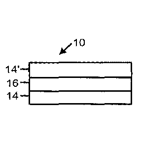
[0013] In some examples, the article 10 can exhibit optical
interference.
Alternatively, in some examples, the article 10 can not exhibit optical
interference.
In an aspect, the article 10 can exploit interference to generate color. In
another
aspect, the article 10 can not exploit interference to generate color. For
example, as
described in further detail below, the appearance of color can be generated by
including a selective light modulator system (SLMS), such as an additive, a
selective
light modulator particle (SLMP) or a selective light modulator molecule (SLMM)
in the
SLML.
3
CA 2971820 2017-06-27
[0014] In an aspect, as shown in Fig. 1, the article 10 can be in a form
of a
sheet that can be used on an object or a substrate 20. In another aspect, the
article
can be in a form of a foil or flake. In an aspect, an optical device can
include
portions of a sheet. In another aspect, an article 10 can include an optical
device
and a liquid medium. In another aspect, the article 10 is an optical device in
the
form of a flake, for example having 100 nm to 100 pm in thickness and 100 nm
to
1mm in size. The article 10 can be a color shifting colorant, or can be used
as a
security feature for currency. Some attributes common to use of the article 10
can
include high chromaticity (or strong color), color change with respect to
viewing
angle (also known as goniochromaticity or iridescence), and flop (a specular
and
metallic appearance that varies in lightness, hue, or chromaticity as the
viewing
angle varies). Additionally, the article 10 can be metallic in color and can
not exploit
interference to generate color.
[0015] Figures 1 and 2 illustrate a sheet including a reflector 16
having a first
surface, a second surface opposite the first surface; and a third surface; a
first
selective light modulator layer 14 external to of the first surface of the
reflector; and a
second selective light modulator layer 14' external to of the second surface
of the
reflector; wherein the third surface (the left and/or right side of reflector
16) of the
reflector is open. Although Figures 1 and 2 illustrate an article 10, such as
an optical
device, in the form of a sheet, the article 10, such as an optical device can
also be in
a form of a flake, and/or a foil, according to various examples of the present
disclosure. Although, Figures 1 and 2 illustrate specific layers in specific
orders, one
of ordinary skill in the art would appreciate that the article 10 can include
any number
of layers in any order. Additionally, the composition of any particular layer
can be
the same or different from the composition of any other layer.
4
CA 2971820 2017-06-27
[0016] The article 10, such as an optical device in the form of a sheet,
flake, or
foil, can include at least one dielectric layer, such as a first SLML 14, a
second SLML
14', a third SLML 14", a fourth SLML 14", and etc. If more than one SLML 14,
14' is
present in an optical device, each SLML can be independent in terms of their
respective compositions and physical properties. For example, a first SLML 14
can
have a composition with a first refractive index, but a second SLML 14' in the
same
optical device can have a different composition with a different refractive
index. As
another example, a first SLML 14 can have a composition at a first thickness,
but the
second SLML 14' can have the same composition at a second thickness different
from the first thickness. Additionally or alternatively, the article 10 in the
form of a
flake, sheet, or foil can also include a hard coat or protective layer on the
surfaces of
SLML 14 and/or SLML 14'. In some examples, these layers (hard coat or
protective
layer) do not require optical qualities.
[0017] As shown in Figures 1 and 2, at least two surfaces/sides of
reflector 16,
for example, the right and left surface/side as shown, can be free of SLMLs
14, 14'.
In an aspect, if the article 10 is in the form of a flake or foil, then
reflector 16 can
include more than the four surfaces exemplified in Figures 1 and 2. In those
instances, for example, one, two, three, four, or five surfaces of reflector
16 can be
free of SLMLs 14. In some examples, one, two, three, four, or five surfaces of
reflector 16, and therefore article 10, can be open to the air. In an example,
open
sides, i.e., surfaces of the reflector that do not contain an external SLML,
can be an
advantage for flop.
[0018] Reflector 16 can be a wideband reflector, e.g., spectral and
Lambertian
reflector (e.g., white TiO2). Reflector 16 can be a metal, non-metal, or metal
alloy. In
one example, the materials for the at least one reflector 16 can include any
materials
CA 2971820 2017-06-27
that have reflective characteristics in the desired spectral range. For
example, any
material with a reflectance ranging from 5% to 100% in the desired spectral
range.
An example of a reflective material can be aluminum, which has good
reflectance
characteristics, is inexpensive, and is easy to form into or deposit as a thin
layer.
Other reflective materials can also be used in place of aluminum. For example,
copper, silver, gold, platinum, palladium, nickel, cobalt, niobium, chromium,
tin, and
combinations or alloys of these or other metals can be used as reflective
materials.
In an aspect, the material for the at least one reflector 16 can be a white or
light
colored metal. In other examples, reflector 16 can include, but is not limited
to, the
transition and lanthanide metals and combinations thereof; as well as metal
carbides, metal oxides, metal nitrides, metal sulfides, a combination thereof,
or
mixtures of metals and one or more of these materials.
[0019] The thickness of the at least one reflector 16 can range from
about 5
nm to about 5000 nm, although this range should not be taken as restrictive.
For
example, the lower thickness limit can be selected so that reflector 16
provides a
maximum transmittance of 0.8. Additionally or alternatively, for a reflector
16
including aluminum the optical density (OD) can be from about 0.1 to about 4
at a
wavelength of about 550 nm.
[0020] In order to obtain a sufficient optical density and/or achieve a
desired
effect, a higher or lower minimum thicknesses can be required depending of the
composition of reflector 16. In some examples, the upper limit can be about
5000
nm, about 4000 nm, about 3000 nm, about1500 nm, about 200 nm, and/or about 100
nm. In one aspect, the thickness of the at least one reflector 16 can range
from
about 10 nm to about 5000 nm for example, from about 15 nm to about 4000 nm,
from about 20 nm to about 3000 nm, from about 25 nm to about 2000 nm, from
6
CA 2971820 2017-06-27
about 30 nm to about 1000 nm, from about 40 nm to about 750 nm, or from about
50
nm to about 500 nm, such as from about 60 nm to about 250 nm or from about 70
nm to about 200 nm.
[0021] The article 10, for example, in the form of a sheet, of Figs. 1
and 2 can
include a first selective light modulator layer (SLML) 14 and a second
selective light
modulator layer 14'. The SLML is a physical layer comprising a plurality of
optical
functions aiming at modulating (absorbing and or emitting) light intensity in
different,
selected regions of spectrum of electromagnetic radiation with wavelengths
ranging
from about 0.2pm to about 20 pm.
[0022] SLMLs 14, 14' (and/or the materials within the SLMLs 14, 14') can
selectively modulate light. For example, an SLML can control the amount of
transmission in specific wavelengths. In some examples, the SLML can
selectively
absorb specific wavelengths of energy (e.g., in the visible and/or non-visible
ranges).
For example, the SLML 14, 14' can be a "colored layer" and/or a "wavelength
selective absorbing layer." In some examples, the specific wavelengths
absorbed
can cause the article 10, for example, in the form of a flake, to appear a
specific
color. For example, the SLML 14, 14' can appear red to the human eye (e.g.,
the
SLML can absorb wavelengths of light below approximately 620 nm and thus
reflect
or transmit wavelengths of energy that appear red). This can be accomplished
by
adding SLMPs that are colorants (e.g., organic and/or inorganic pigments
and/or
dyes) to a host material, such as a dielectric material, including but not
limited to a
polymer. For example, in some instances, the SLML can be a colored plastic.
[0023] In some examples, some or all of the specific wavelengths
absorbed
can be in the visible range (e.g., the SLML can be absorbing throughout the
visible,
but transparent in the infrared). The resulting article 10, for example in the
form of a
7
CA 2971820 2017-06-27
flake, would appear black, but reflect light in the infrared. In some examples
described above, the wavelengths absorbed (and/or the specific visible color)
of the
article 10 and/or SLML 14, 14' can depend, at least in part, on the thickness
of the
SLML 14, 14'. Additionally or alternatively, the wavelengths of energy
absorbed by
the SLML 14, 14' (and/or the color in which these layers and/or the flake
appears)
can depend in part on the addition of certain aspects to the SLML. In addition
to
absorbing certain wavelengths of energy, the SLML 14, 14' can achieve at least
one
of bolstering the reflector 16 against degradation; enabling release from a
substrate;
enabling sizing; providing some resistance to environmental degradation, such
as
oxidation of aluminum or other metals and materials used in the reflector 16;
and
high performance in transmission, reflection, and absorption of light based
upon the
composition and thickness of the SLML 14, 14'.
[0024] In some examples, in addition to or as an alternative to the
SLMLs 14,
14' selectively absorbing specific wavelengths of energy and/or wavelengths of
visible light, the SLMLs 14, 14' of the article 10, for example in the form of
a sheet,
can control the refractive index and/or the SLMLs 14, 14' can include SLMPs
that
can control refractive index. SLMPs that can control the refractive index of
the SLML
14, 14' can be included with the host material in addition to or as an
alternative to an
absorption controlling SLMPs (e.g., colorants). In some examples, the host
material
can be combined with both absorption controlling SLMPs and refractive index
SLMPs in the SLMLs 14, 14'. In some examples, the same SLMP can control both
absorption and refractive index.
[0025] The performance of the SLML 14, 14' can be determined based upon
the selection of materials present in the SLML14, 14'. In an aspect, the SLML
14,
14' can improve at least one of the following properties: flake handling,
corrosion,
8
CA 2971820 2017-06-27
alignment, and environmental performance of any other layers within article
10, e.g.,
the reflector 16.
[0026] The first and second SLML 14, 14' can each independently comprise
a
host material alone, or a host material combined with a selective light
modulator
system (SLMS). In an aspect, at least one of the first SLML 14 and the second
SLML 14' includes a host material. In another aspect, at least one of the
first SLML
14 and the second SLML 14' includes a host material and a SLMS. The SLMS can
include a selective light modulator molecule (SLMM), a selective light
modulator
particle (SLMP), an additive, or combinations thereof.
[0027] The composition of the SLML 14, 14' can have a solids content
ranging
from about 0.01% to about 100%, for example from about 0.05% to about 80%, and
as a further example from about 1% to about 30%. In some aspects, the solids
content can be greater than 3%. In some aspects, the composition of the SLMLs
14,
14' can have a solids content ranging from about 3% to about 100%, for example
from about 4% to 50%.
[0028] The host material of each of the first and/or second SLMLs 14,
14' can
independently be a film forming material applied as a coating liquid and
serving
optical and structural purposes. The host material can be used as a host
(matrix) for
introducing, if necessary, a guest system, such as the selective light
modulator
system (SLMS), for providing additional light modulator properties to the
article 10.
[0029] The host material can be a dielectric material. Additionally or
alternatively, the host material can be at least one of an organic polymer, an
inorganic polymer, and a composite material. Non-limiting examples of the
organic
polymer include thermoplastics, such as polyesters, polyolefins,
polycarbonates,
polyamides, polyimides, polyurethanes, acrylics, acrylates, polyvinylesters,
9
CA 2971820 2017-06-27
polyethers, polythiols, silicones, fluorocarbons, and various co-polymers
thereof;
thermosets, such as epoxies, polyurethanes, acrylates, melamine formaldehyde,
urea formaldehyde, and phenol formaldehyde; and energy curable materials, such
as acrylates, epoxies, vinyls, vinyl esters, styrenes, and silanes. Non-
limiting
examples of inorganic polymers includes silanes, siloxanes, titanates,
zirconates,
aluminates, silicates, phosphazanes, polyborazylenes, and polythiazyls.
[0030] Each of the first and second SLMLs 14, 14' can include from about
0.001% to about 100% by weight of a host material. In an aspect, the host
material
can be present in the SLML in an amount ranging from about 0.01% to about 95%
by
weight, for example from about 0.1% to about 90%, and as a further example
from
about 1% to about 87% by weight of the SLML.
[0031] The SLMS, for use in the SLMLs 14, 14' with the host material,
can
each independently comprise selective light modulator particles (SLMP),
selective
light modulator molecules (SLMM), additives, or a combination thereof. The
SLMS
can also comprise other materials. The SLMS can provide modulation of the
amplitude of electromagnetic radiation (by absorption, reflectance,
fluorescence etc.)
in a selective region or the entire spectral range of interest (0.2 pm to 20
pm).
[0032] The first and second SLMLs 14, 14' can each independently include
in
an SLMS a SLMP. The SLMP can be any particle combined with the host material
to selectively control light modulation, including, but not limited to color
shifting
particles, dyes, colorants includes colorant includes one or more of dyes,
pigments,
reflective pigments, color shifting pigments, quantum dots, and selective
reflectors.
Non-limiting examples of a SLMP include: organic pigments, inorganic pigments,
quantum dots, nanoparticles (selectively reflecting and/or absorbing),
micelles, etc.
The nanoparticles can include, but are not limited to organic and metalorganic
CA 2971820 2017-06-27
materials having a high value of refractive index (n > 1.6 at wavelength of
about 550
nm); metal oxides, such as TiO2, ZrO2, In203, 1n203-SnO, Sn02, FeO y (wherein
x
and y are each independently integers greater than 0), and W03; metal
sulfides,
such as ZnS, and Cu,Sy (wherein x and y are each independently integers
greater
than 0); chalcogenides, quantum dots, metal nanoparticles; carbonates;
fluorides;
and mixtures thereof.
[0033] Examples of a SLMM include but are not limited to: organic dyes,
inorganic dyes, micelles, and other molecular systems containing a
chromophore.
[0034] In some aspects, SLMS of each of the first and second SLMLs 14,
14'
can include at least one additive, such as a curing agent, and a coating aid.
[0035] The curing agent can be a compound or material that can initiate
hardening, vitrification, crosslinking, or polymerizing of the host material.
Non-
limiting examples of a curing agent include solvents, radical generators (by
energy or
chemical), acid generators (by energy or chemical), condensation initiators,
and
acid/base catalysts.
[0036] Non-limiting examples of the coating aid include leveling agents,
wetting agents, defoamers, adhesion promoters, antioxidants, UV stabilizers,
curing
inhibition mitigating agents, antifouling agents, corrosion inhibitors,
photosensitizers,
secondary crosslinkers, and infrared absorbers for enhanced infrared drying.
In an
aspect, the antioxidant can be present in the composition of the SLML 14, 14'
in an
amount ranging from about 25 ppm to about 5% by weight.
[0037] The first and second SLMLs 14, 14' can each independently
comprise
a solvent. Non-limiting examples of solvents can include acetates, such as
ethyl
acetate, propyl acetate, and butyl acetate; acetone; water; ketones, such as
dimethyl
ketone (DMK), methylethyl ketone (MEK), secbutyl methyl ketone (SBMK), ter-
butyl
11
CA 2971820 2017-06-27
methyl ketone (TBMK), cyclopenthanon, and anisole; glycol and glycol
derivatives,
such as propylene glycol methyl ether, and propylene glycol methyl ether
acetate;
alcohols, such as isopropyl alcohol, and diacetone alcohol; esters, such as
malonates; heterocyclic solvents, such as n-methyl pyrrolidone; hydrocarbons,
such
as toluene, and xylene; coalescing solvents, such as glycol ethers; and
mixtures
thereof. In an aspect, the solvent can be present in each of the first and
second
SLML 14, 14' in an amount ranging from about 0% to about 99.9%, for example
from
about 0.005% to about 99%, and as a further example from about 0.05% to about
90% by weight relative to the total weight of the SLML 14, 14'.
[0038] In some examples, the first and second SLML 14, 14' can each
independently include a composition having at least one of (i) a
photoinitiator, (ii) an
oxygen inhibition mitigation composition, (iii) a leveling agent, and (iv) a
defoamer.
[0039] The oxygen inhibition mitigation composition can be used to
mitigate
the oxygen inhibition of the free radical material. The molecular oxygen can
quench
the triplet state of a photoinitiator sensitizer or it can scavenge the free
radicals
resulting in reduced coating properties and/or uncured liquid surfaces. The
oxygen
inhibition mitigation composition can reduce the oxygen inhibition or can
improve the
cure of any SLML 14, 14'.
[0040] The oxygen inhibition composition can comprise more than one
compound. The oxygen inhibition mitigation composition can comprise at least
one
acrylate, for example at least one acrylate monomer and at least one acrylate
oligomer. In an aspect, the oxygen inhibition mitigation composition can
comprise at
least one acrylate monomer and two acrylate oligomers. Non-limiting examples
of
an acrylate for use in the oxygen inhibition mitigation composition can
include
acrylates; methacrylates; epoxy acrylates, such as modified epoxy acrylate;
12
CA 2971820 2017-06-27
polyester acrylates, such as acid functional polyester acrylates, tetra
functional
polyester acrylates, modified polyester acrylates, and bio-sourced polyester
acrylates; polyether acrylates, such as amine modified polyether acrylates
including
amine functional acrylate co-initiators and tertiary amine co-initiators;
urethane
acrylates, such aromatic urethane acrylates, modified aliphatic urethane
acrylates,
aliphatic urethane acrylates, and aliphatic allophanate based urethane
acrylates; and
monomers and oligomers thereof. In an aspect, the oxygen inhibition mitigation
composition can include at least one acrylate oligomer, such as two oligomers.
The
at least one acrylate oligomer can be selected/chosen from a polyester
acrylate and
a polyether acrylate, such as a mercapto modified polyester acrylate and an
amine
modified polyether tetraacrylate. The oxygen inhibition mitigation composition
can
also include at least one monomer, such as 1,6-hexanediol diacrylate. The
oxygen
inhibition mitigation composition can be present in the first and/or second
SLML 14,
14' in an amount ranging from about 5% to about 95%, for example from about
10%
to about 90%, and as a further example from about 15% to about 85% by weight
relative to the total weight of the SLML 14, 14'.
[0041] In some examples, the host material of the SLML 14, 14' can use a
non-radical cure system such as a cationic system. Cationic systems are less
susceptible to the mitigation of the oxygen inhibition of the free radical
process, and
thus may not require an oxygen inhibition mitigation composition. In an
example,
the use of the monomer 3-Ethyl-3-hydroxymethyloxetane does not require an
oxygen mitigation composition.
[0042] In an aspect, the first and second SLML 14, 14' can each
independently include at least one photoinitiator, such as two
photoinitiators, or three
photoinitiators. The photoinitiator can be used for shorter wavelengths. The
13
CA 2971820 2017-06-27
photoinitiator can be active for actinic wavelength. The photoinitiator can be
a Type
1 photoinitiator or a Type II photoinitiator. The SLML 14, 14' can include
only Type I
photoinitiators, only Type ll photoinitiators, or a combination of both Type I
and Type
II photoinitiators. The photoinitiator can be present in the composition of
the SLML
14, 14' in an amount ranging from about 0.25% to about 15%, for example from
about 0.5% to about 10%, and as a further example from about 1% to about 5% by
weight relative to the total weight of the composition of the SLML 14, 14'.
[0043] The photoinitiator can be a phosphineoxide. The phosphineoxide
can
include, but is not limited to, a monoacyl phosphineoxide and a bis acyl
phosphine
oxide. The mono acyl phosphine oxide can be a diphenyl (2,4,6-
trimethylbenzoyl)phosphineoxide. The bis acyl phosphine oxide can be a bis
(2,4,6-
trimethylbenzoyl)phenylphosphineoxide. In an aspect, at least one
phosphineoxide
can be present in the composition of the SLML 14, 14'. For example, two
phosphineoxides can be present in the composition of the SLML 14, 14'.
[0044] A sensitizer can be present in the composition of the SLML 14,
14' and
can act as a sensitizer for Type 1 and/or a Type II photoinitiators. The
sensitizer can
also act as a Type II photoinitiator. In an aspect, the sensitizer can be
present in the
composition of the SLML 14, 14' in an amount ranging from about 0.05% to about
10%, for example from about 0.1% to about 7%, and as a further example from
about 1% to about 5% by weight relative to the total weight of the composition
of the
SLML 14, 14'. The sensitizer can be a thioxanthone, such as 1-chloro-4-
propoxythioxanthone.
[0045] In an aspect, the SLML 14, 14' can include a leveling agent. The
leveling agent can be a polyacrylate. The leveling agent can eliminate
cratering of
the composition of the SLML 14, 14'. The leveling agent can be present in the
14
CA 2971820 2017-06-27
composition of the SLML 14, 14' in an amount ranging from about 0.05% to about
10%, for example from about 1% to about 7%, and as a further example from
about
2% to about 5% by weight relative to the total weight of the composition of
the SLML
14, 14'.
[0046] The SLML 14, 14' can also include a defoamer. The defoamer can
reduce surface tension. The defoamer can be a silicone free liquid organic
polymer.
The defoamer can be present in the composition of the SLML 14, 14' in an
amount
ranging from about 0.05% to about 5%, for example from about 0.2% to about 4%,
and as a further example from about 0.4% to about 3% by weight relative to the
total
weight of the composition of the SLML 14, 14'.
[0047] The first and second SLML 14, 14' can each independently have a
refractive index of greater or less than about 1.5. For example, each SLML 14,
14'
can have a refractive index of approximately 1.5. The refractive index of each
SLML
14, 14' can be selected to provide a degree of color travel required wherein
color
travel can be defined as the change in hue angle measured in L*a*b* color
space
with the viewing angle. In some examples, each SLMLs 14, 14' can include a
refractive index in a range of from about 1.1 to about 3.0, about 1.0 to about
1.3, or
about 1.1 to about 1.2. In some examples, the refractive index of each SLMLs
14,
and 14' can be less than about 1.5, less than about 1.3, or less than about
1.2. In
some examples, SLML 14 and SLML 14' can have substantially equal refractive
indexes or different refractive indexes one from the other.
[0048] The first and second SLML 14, 14' can each independently have a
thickness ranging from about 1 nm to about 10000 nm, about 10 nm to about 1000
nm, about 20 nm to about 500 nm, about 1 nm, to about 100 nm, about 10 nm to
about 1000 nm, about 1 nm to about 5000 nm. In an aspect, the article 10, such
as
CA 2971820 2017-06-27
an optical device, can have an aspect ratio of 1:1 to 1:50 thickness to width.
[0049] One of the benefits of the articles 10 described herein, however,
is that,
in some examples, the optical effects appear relatively insensitive to
thickness
variations. Thus, in some aspects, each SLML 14, 14' can independently have a
variation in optical thickness of less than about 5%. In an aspect, each SLML
14, 14'
can independently include an optical thickness variation of less than about 3%
across the layer. In an aspect, each SLML 14, 14' can independently have less
than
about 1% variation in optical thickness across the layer having a thickness of
about
50 nm.
[0050] In an aspect, the article 10, such as an optical device in the
form of a
flake, foil or sheet, can also include a substrate 20 and a release layer 22
as shown
in Fig. 2. In an aspect, the release layer 22 can be disposed between the
substrate
20 and the first SLML 14.
[0051] The article 10, such as optical devices, described herein can be
made
in any way. For example, a sheet (e.g., article 10 of Figs. 1 and 2) can be
made
and then divided, broken, ground, etc. into smaller pieces forming an optical
device.
In some examples, the sheet (e.g., article 10 of Figs. 1 and 2) can be created
by a
liquid coating process, including, but not limited the processes described
below
and/or with respect to Fig. 3.
[0052] There is disclosed a method for manufacturing an article 10, for
example in the form of a sheet, flake, or foil, as described herein. The
method can
comprise depositing on a substrate a first SLML; depositing on the first SLML
at least
one reflector; and depositing on the at least one reflector a second SLML;
wherein at
least one of the first SLML and the second SLML is deposited using a liquid
coating
process.
16
CA 2971820 2017-06-27
[0053] With respect to the aspects shown in Figs. 1 and 2, article 10,
such as
an optical device, in the form of a flake, sheet, or foil, can be created by
depositing
the first SLML 14 on a substrate 20. The substrate 20 can comprise a release
layer
22. In an aspect, as shown in Fig. 2, the method can include depositing on the
substrate 20, having release layer 22, the first SLML 14, and depositing on
the first
SLML 14 at least one reflector 16. The method further includes depositing on
the at
least one reflector 16, a second SLML 14'. In some examples, the at least one
reflector 16 can be applied to the respective layers by any known conventional
deposition process, such as physical vapor deposition, chemical vapor
deposition,
thin-film deposition, atomic layer deposition, etc., including modified
techniques such
as plasma enhanced and fluidized bed.
[0054] The substrate 20 can be made of a flexible material. The
substrate 20
can be any suitable material that can receive the deposited layers. Non-
limiting
examples of suitable substrate materials include polymer web, such as
polyethylene
terephthalate (PET), glass foil, glass sheets, polymeric foils, polymeric
sheets, metal
foils, metal sheets, ceramic foils, ceramic sheets, ionic liquid, paper,
silicon wafers,
etc. The substrate 20 can vary in thickness, but can range for example from
about 2
pm to about 100 pm, and as a further example from about 10 to about 50 pm.
[0055] The first SLML 14 can be deposited on the substrate 20 by a
liquid
coating process, such as a slot die process. Once the first SLML 14 has been
deposited and cured, the at least one reflector 16 can be deposited on the
first SLML
14 using any conventional deposition processes described above. After the at
least
one reflector 16 has been deposited on the first SLML 14, the second SLML 14'
can
be deposited on the at least one reflector 16 via a liquid coating apparatus,
such as a
slot die apparatus. The liquid coating process includes, but is not limited
to: slot-
17
CA 2971820 2017-06-27
bead, slide bead, slot curtain, slide curtain, in single and multilayer
coating,
tensioned web slot, gravure, roll coating, and other liquid coating and
printing
processes that apply a liquid on to a substrate to form a liquid layer or film
that is
subsequently dried and/or cured to the final SLML layer.
[0056] The substrate 20 can then be released from the deposited layers
to
create the article 10, for example as shown in Fig. 1. In an aspect, the
substrate 20
can be cooled to embrittle the associated release layer 22. In another aspect,
the
release layer 22 could be embrittled for example by heating and/or curing with
photonic or e-beam energy, to increase the degree of cross-linking, which
would
enable stripping. The deposited layers can then be stripped mechanically, such
as
sharp bending or brushing of the surface. The released and stripped layers can
be
sized into article 10, such as an optical device in the form of a flake, foil,
or sheet,
using known techniques.
[0057] In another aspect, the deposited layers can be transferred from
the
substrate 20 to another surface. The deposited layers can be punched or cut to
produce large flakes with well-defined sizes and shapes.
[0058] As stated above, each of the first and second SLML 14, 14' can be
deposited by a liquid coating process, such as a slot die process. However, it
was
previously believed that liquid coating processes, such as a slot die process,
could
not operate stably at optical thicknesses, such as from about 50 to about 700
nm. In
particular thin, wet films have commonly formed islands of thick areas where
solids
have been wicked away from the surrounding thin areas by capillary forces as
solvents evaporate. This reticulated appearance is not compatible with optical
coatings as the variable thickness can result in a wide range of optical path
lengths,
such as a side range of colors resulting in a speckled/textured appearance, as
well
18
CA 2971820 2017-06-27
as reduced color uniformity of the optical coating and low chromaticity.
[0059] In an aspect of the present disclosure, the SLML 14, 14' can be
formed
using a liquid coating process, such as a slot die process. In an aspect, the
liquid
coating process includes, but is not limited to: slot-bead, slide bead, slot
curtain,
slide curtain, in single and multilayer coating, tensioned web slot, gravure,
roll
coating, and other liquid coating and printing processes that apply a liquid
on to a
substrate to form a liquid layer or film that is subsequently dried and/or
cured to the
final SLML layer. . The liquid coating process can allow for the transfer of
the
composition of the SLML 14, 14' at a faster rate as compared to other
deposition
techniques, such as vapor deposition.
[0060] Additionally, the liquid coating process can allow for a wider
variety of
materials to be used in the SLML 14, 14' with a simple equipment set up. It is
believed that the SLML 14, 14' formed using the disclosed liquid coating
process can
exhibit improved optical performance.
[0061] Fig. 3 illustrates the formation of the SLML 14, 14' using a
liquid
coating process. The composition of the SLML (a liquid coating composition)
can be
inserted into a slot die 320 and deposited on a substrate 340 resulting in a
wet film.
With reference to the processes disclosed above, the substrate 340 can include
the
substrate 20, with or without a release layer 22; the substrate 340 can
include the
substrate 20, with or without a release layer 22, a first SLML 14, and the at
least one
reflector 16; or the substrate 340 can include any combination of substrate
20,
release layer 22, and deposited layers. The distance from the bottom of the
slot die
320 to the substrate 340 is the slot gap G. As can be seen in Fig. 3, the
liquid
coating composition can be deposited at a wet film thickness D that is greater
than a
dry film thickness H. After the wet film of the SLML 14, 14' has been
deposited on
19
CA 2971820 2017-06-27
the substrate 340, any solvent present in the wet film of the SLML 14, 14' can
be
evaporated. The liquid coating process continues with curing of the wet film
of the
SLML 14, 14' to result in a cured, self-leveled SLML 14, 14' having the
correct optical
thickness H (ranging from about 30 to about 700 nm). It is believed that the
ability of
the SLML 14, 14' to self-level results in a layer having a reduced optical
thickness
variation across the layer. Ultimately, an article 10, such as an optical
device,
comprising the self-leveled SLML 14, 14' can exhibit increased optical
precision. For
ease of understanding, the terms "wet film" and "dry film" will be used to
refer to the
composition at various stages of the liquid coating process that results in
the SLML
14, 14'.
[0062] The liquid coating process can comprise adjusting at least one of
a
coating speed and a slot gap G to achieve a wet film with a predetermined
thickness
D. The SLML 14, 14' can be deposited having a wet film thickness D ranging
from
about 0.1 pm to about 500 pm, for example from about 0.1 pm to about 5 pm. The
SLML 14,14' formed with a wet film thickness D in the disclosed range can
result in a
stable SLML layer, such as a dielectric layer, i.e., without breaks or defects
such as
ribbing or streaks. In an aspect, the wet film can have a thickness of about
10 pm for
a stable wet film using a slot die bead mode with a coating speed up to about
100
m/min. In another aspect, the wet film can have a thickness of about 6-7 pm
for a
stable wet film using a slot die curtain mode with a coating speed up to about
1200
m/min.
[0063] The liquid coating process can include a ratio of slot gap G to
wet film
thickness D of about 1 to about 100 at speeds from about 0.1 to about 1000
m/min.
In an aspect, the ratio is about 9 at a coating speed of about 100 m/min. In
an
aspect, the ratio can be about 20 at a coating speed of about 50 m/min. The
liquid
CA 2971820 2017-06-27
coating process can have a slot gap G ranging from about 0 to about 1000 pm. A
smaller slot gap G can allow for a reduced wet film thickness. In slot-bead
mode
higher coating speeds can be achieved with a wet film thickness greater than
10 pm.
[0064] The liquid coating process can have a coating speed ranging from
about 0.1 to about 1000 m/min, for example from about 25 m/min to about 950
m/min, for example from about 100 m/rnin to about 900 m/min, and as a further
example from about 200 m/min to about 850 rn/rnin. In an aspect, the coating
speed
is greater than about 150 m/min, and in a further example is greater than
about 500
m/nnin.
[0065] In an aspect, the coating speed for a bead mode liquid coating
process
can range from about 0.1 rri/min to about 600 m/min, and for example from
about 50
to about 150 m/min. In another aspect, the coating speed for a curtain mode
liquid
coating process can range from about 200 rrilmin to about 1500 m/min, and for
example
from about 300 m/min to about 1200 m/min.
[0066] As shown in Fig. 3 the solvent can be evaporated from the wet
film,
such as before the wet film is cured. In an aspect, about 100%, for example
about
99.9%, and as a further example about 99.8% of the solvent can be evaporated
from
the composition of the SLML 14, 14, prior to curing of the SLML 14, 14'. In a
further
aspect, trace amounts of solvent can be present in a cured/dry SLML 14, 14'.
In an
aspect, a wet film having a greater original weight percent of solvent can
result in a
dry film having a reduced film thickness H. In particular, a wet film having a
high
weight percent of solvent and being deposited at a high wet film thickness D
can
result in a SLML 14, 14' having a low dry film thickness H. It is important to
note,
that after evaporation of the solvent, the wet film remains a liquid thereby
avoiding
21
CA 2971820 2017-06-27
problems such as skinning, and island formation during the subsequent curing
steps
in the liquid coating process.
[0067] The dynamic viscosity of the wet film can range from about 0.5 to
about
50 cP, for example from about 1 to about 45 cP, and as a further example from
about 2 to about 40 cP. The viscosity measurement temperature is 25 C, the
rheology was measured with an Anton Paar MCR 101 rheometer equipped with a
solvent trap using a cone/plate 40mm diameter with 0.3 angle at a gap setting
of
0.025 mm.
[0068] In an aspect, the composition of the SLML 14, 14' and the solvent
can
be selected so that the wet film exhibits Newtonian behavior for precision
coating of
the SLMLs using the liquid coating process. The wet film can exhibit Newtonian
behavior shear rates up to 10,000 s-1 and higher. In an aspect, the shear rate
for the
liquid coating process can be 1000 s-1 for a coating speed up to 25 m/min, for
example 3900 s-1 for a coating speed up to 100 m/min, and as a further example
7900 s-1 for a coating speed up to 200 m/min. It will be understood that a
maximum
shear rate can occur on a very thin wet film, such as 1 pm thick.
[0069] As the wet film thickness is increased, the shear rate can be
expected
to decrease, for example decrease 15% for a 10 pm wet film, and as a further
example decrease 30% for a 20 pm wet film.
[0070] The evaporation of the solvent from the wet film can cause a
change in
viscosity behavior to pseudoplastic, which can be beneficial to achieve a
precision
SLML. The dynamic viscosity of the deposited first and second SLML 14, 14',
after
any solvent has been evaporated, can range from about 10 cP to about 3000 cP,
for
example from about 20 cP to about 2500cP, and as a further example from about
30
cP to about 2000 cP. When evaporating the solvent, if present, from the wet
film
22
CA 2971820 2017-06-27
there can be an increase in viscosity to the pseudoplastic behavior. The
pseudoplastic behavior can allow for self-leveling of the wet film.
[0071] In an aspect, the method can include evaporating the solvent
present
in the wet film using known techniques. The amount of time required to
evaporate
the solvent can be dependent upon the speed of the web/substrate and the dryer
capacity. In an aspect, the temperature of the dryer (not shown) can be less
than
about 120 C, for example less than about 100 C, and as a further example
less
than about 80 C.
[0072] The wet film deposited using a liquid coating process can be
cured
using known techniques. In an aspect, the wet film can be cured using a curing
agent utilizing at least one of a ultraviolet light, visible light, infrared,
or electron
beam. Curing can proceed in an inert or ambient atmosphere. In an aspect, the
curing step utilizes an ultraviolet light source having a wavelength of about
395 nm.
The ultraviolet light source can be applied to the wet film at a dose ranging
from
about 200 mJ/cm2 to about 1000 mJ/cm2, for example ranging from about 250
mJ/cm2 to about 900 mJ/cm2, and as a further example from about mJ/cm2 to
about
850 mJ/cm2.
[0073] The wet film can crosslink by known techniques. Non-limiting
examples include photoinduced polymerization, such as free radical
polymerization,
spectrally sensitized photoinduced free radical polymerization, photoinduced
cationic
polymerization, spectrally sensitized photoinduced cationic polymerization,
and
photoinduced cycloaddition; electron beam induced polymerization, such as
electron
beam induced free radical polymerization, electron beam induced cationic
polymerization, and electron beam induced cycloaddition; and thermally induced
polymerization, such as thermally induced cationic polymerization.
23
CA 2971820 2017-06-27
[0074] A SLML 14, 14' formed using the liquid coating process can
exhibit
improved optical performance, i.e., be a precision SLML. In some examples, a
precision SLML 14, 14' can be understood to mean a SLML having less than about
3% optical thickness variation, about 5% optical thickness variation, or about
7%
optical thickness variation across the layer.
[0075] In an aspect, the liquid coating process can include adjusting at
least
one of speed from about 5 to about 100m/min and a coating gap from about 50 pm
to about 100 pm to deposit a wet film from about 2 pm to 10 pm of the
selective light
modulator layer with a predetermined thickness from about 500 nm to about 1500
nm. In a further aspect, the process can include a speed of 30m/min, a 75 urn
gap,
urn wet film, dry film thickness 1.25 urn.
[0076] In an example, the SLML includes a alicyclic epoxy resin host
using a
solvent dye as the SLMM, the reflector includes aluminum.
[0077] In an example, the SLML includes a alicyclic epoxy resin host
using a
Diketopyrrolopyrrole insoluble red dye as the SLMP, the reflector includes
aluminum.
[0078] In an example, the SLML includes an acrylate oligomer resin host
using white pigment (Titania) as the SLMP.
[0079] In an example, the SLML includes an acrylate oligomer resin host
using black IR transparent pigment as the SLML, the reflector includes
aluminum.
[0080] From the foregoing description, those skilled in the art can
appreciate
that the present teachings can be implemented in a variety of forms.
Therefore,
while these teachings have been described in connection with particular
embodiments and examples thereof, the true scope of the present teachings
should
not be so limited. Various changes and modifications can be made without
departing
from the scope of the teachings herein.
24
CA 2971820 2017-06-27
[0081] This scope disclosure is to be broadly construed. It is intended
that
this disclosure disclose equivalents, means, systems and methods to achieve
the
devices, activities and mechanical actions disclosed herein. For each device,
article,
method, mean, mechanical element or mechanism disclosed, it is intended that
this
disclosure also encompass in its disclosure and teaches equivalents, means,
systems and methods for practicing the many aspects, mechanisms and devices
disclosed herein. Additionally, this disclosure regards a coating and its many
aspects, features and elements. Such a device can be dynamic in its use and
operation, this disclosure is intended to encompass the equivalents, means,
systems
and methods of the use of the device and/or optical device of manufacture and
its
many aspects consistent with the description and spirit of the operations and
functions disclosed herein. The claims of this application are likewise to be
broadly
construed. The description of the inventions herein in their many embodiments
is
merely exemplary in nature and, thus, variations that do not depart from the
gist of
the invention are intended to be within the scope of the invention. Such
variations
are not to be regarded as a departure from the spirit and scope of the
invention.
CA 2971820 2017-06-27