Note: Descriptions are shown in the official language in which they were submitted.
CA 02974044 2017-07-17
WO 2016/128133
PCT/EP2016/000220
1
Optoelectronic devices comprising solution-proces sable
metal oxide buffer, layers
The present invention relates to the field of electronic
devices, particularly optoelectronic devices. The
invention further provides intermediate goods and
materials suitable for manufacturing such devices, the
invention also provides for specific manufacturing methods
and for specific uses.
It is known to use buffer layers in organic electronics,
such as organic light emitting diodes (OLED), organic
photovoltaic cells (OPV cells) or perovskite type solar
cells, in order to increase device efficiency and life-
time. Such buffer layers comprise metal oxides, such as
zinc-, titanium-, tungsten-, nickel-, niobium- oxides, or
doped metal oxides, such as Al-doped ZnO ("AZO") or Cu-
doped NiO. Generally, such metal oxides in particulate form
are known. Typically, the above named oxidic buffer layers
are manufactured by thermal evaporation under high vacuum
or by wet-chemical (precursor based) methods, requiring a
high temperature annealing step; which is disadvantageous
in terms of low-cost, large-area manufacturing processing.
It is also known that organic solar cells (OPV) offer a
promising approach for a low-cost and flexible photovoltaic
technology with certified efficiencies exceeding 10%.
Before widespread commercialization, large area production
and stability issues have to be solved. For the reliable
large area production with high yield and low shunts,
thick, stable, robust and printable buffer layers are a
prerequisite.
Generally, such metal oxides in particulate form are known.
As discussed above, such oxidic layers are manufactured by
thermal evaporation under high vacuum; which is
disadvantageous in terms of low-cost, large-area
manufacturing processing. Such processes,
using
CA 02974044 2017-07-17
WO 2016/128133
PCT/EP2016/000220
2
comparatively high temperatures, e.g. by including an
annealing step, are also disadvantageous in case the layer
preceding the buffer layer is temperature sensitive. The
present inventors thus identified a need to provide
manufacturing processes for buffer layers, particularly
metal oxide buffer layers, that are compatible with
temperature sensitive layers / materials.
It is also known that Cs2CO3 significantly influences work
function of metal oxides in buffer layers. In certain
applications, this is considered disadvantageous, as the
desired properties of metal oxides interfere with the
properties of Cs2003. The present inventors thus identified
a need to provide metal oxide buffer layers with low or
even zero amounts of Cs2CO3.
Luechinger et al. (W02014/161100) describe organic
electronic devices, such as OLEDs and organic solar cells,
comprising buffer layers with surface modified metal oxide
nanoparticles. Further, the advantages of solution
processable buffer layers are outlined. Although simple in
manufacturing, through its all-solution-process, the
devices disclosed therein show comparatively low
performance.
Kim et al. (Adv. Mater., 2014, DOI: 10.1002/adma.201404189)
describe perovskite-type organic solar cells comprising
NiO and Cu-doped NiO buffer layers. Due to its
manufacturing, the buffer layers are dense, i.e. not
particulate. The devices show performances exceeding 15%
PCE. Nevertheless it is considered disadvantageous that
the metal oxide layers are applied by a wet chemical
(precursor based) method and thus need to be thermally
cured at very high temperatures. Accordingly, these devices
are more difficult in manufacturing, as the remaining
layers of the solar cells cannot withstand such high
temperatures and thus need to be coated after the
deposition of the buffer layer.
CA 02974044 2017-07-17
WO 2016/128133
PCT/EP2016/000220
3
Liu et al. (Chem. of Mater., 2014, DOI: 10.1021/cm501898y)
describe OLEDs comprising NiO hole transport layers. Again,
due to its manufacturing, the buffer layers described in
this document are dense and not particulate. It is further
described that these precursor based layers need to be
cured at temperatures of at least 275 C and even as high
as 500 C. Again, this is considered obstructive to the
successful production of organic material based electronic
devices.
Kim et al (Nanoscale Research Letters 2014, 9, 323) discuss
the effect of ZnO:Cs2CO3 on the performance of organic
photovoltaics. As stated in that document, the work
function of ITO is decreased from 4.7eV to 3.8eV due to
the modification by Cs2CO3. Such modification of the work
function may, depending on the application, be beneficial
or disadvantageous.
Yang et al (US2010/0012178) describe solution processable
materials for electronic and electro-optic applications.
To that end, the electro-optic device comprises an
interfacial layer which is a blend of a metal oxide and at
least one other material that provides at least one of a
decrease in the work function or an increase of electrical
conductivity compared to the metal oxide alone. Such other
material being present in amounts of at least 10% and up
to 120% and thus significantly influence the properties of
the metal oxide.
Dong et al (RSC Adv 2014, 4, 60131) discloses the use of
Cs2CO3 as surface modification material for hybrid
perovskite solar cells.
Thus, it is an object of the present invention to mitigate
at least some of these drawbacks of the state of the art.
In particular, it is an aim of the present invention to
provide compositions suitable for thin film formation on a
plurality of substrates. It is a further aim to provide
CA 02974044 2017-07-17
WO 2016/128133
PCT/EP2016/000220
4
manufacturing methods for thin films avoiding vapor phase
processes and to provide improved electrical devices and
intermediate goods. It is a still further aim to provide
optoelectronic devices, and components therefore, that are
high performing. It is a still further aim to provide
optoelectronic devices, and components therefore, which
are simple in manufacturing.
These objectives are achieved by a device as defined in
claim 1 and an intermediate good as defined in claim 10
and the uses as defined in claim 13. Further aspects of
the invention are disclosed in the specification and
independent claims, preferred embodiments are disclosed in
the specification and the dependent claims.
The present invention will be described in detail below.
It is understood that the various embodiments, preferences
and ranges as provided / disclosed in this specification
may be combined at will. Further, depending of the specific
embodiment, selected definitions, embodiments or ranges
may not apply.
Unless otherwise stated, the following definitions shall
apply in this specification:
The terms "a", "an", "the" and similar terms used in the
context of the present invention are to be construed to
cover both the singular and plural unless otherwise
indicated herein or clearly contradicted by the context.
Further, the terms "including", "containing" and
"comprising" are used herein in their open, non-limiting
sense. The term "containing" shall include both,
"comprising" and "consisting of".
Percentages are given as weight-%, unless otherwise
indicated herein or clearly contradicted by the context.
The term "electronic device" is known in the field. In the
context of the present invention, any device comprising
CA 02974044 2017-07-17
WO 2016/128133
PCT/EP2016/000220
functional thin films is encompassed, including inorganic
LEDs or inorganic solar cells; but specifically organic
electronics as defined below.
5 The term "optoelectronic device" is known in the field and
denotes electronic devices that source, detect or control
light. Accordingly, such devices either convert an
electrical signal into an optical signal or vice versa.
The terms "organic electronics", "organic electronic
devices", "OLED", "OPV" are known in the field and relate
to electronic devices comprising a "substrate" and a
multitude of layers, wherein at least one layer is a
"buffer layer" as defined below. In organic electronics at
least one layer comprises organic substances, essential to
the correct functioning of said devices. Depending on the
remaining layers, its structure and connection, these
devices serve a multitude of purposes, such as an OLED, an
OPV cell, organic photo detector, or perovskite solar cell.
The term LED comprises both, organic LEDs (OLEDs) where
the active layer comprises organic electrolumineszent
materials (polymers or small molecule), and Quantum dot
LEDs (QLEDs), where the active layer comprises
electrolumineszent quantum dots.
The term "Buffer layer" denotes an interface layer in
electronic devices, typically in devices as discussed
herein. Buffer layer is the general term for layers with a
charge selective function such as hole transport (HTL),
hole injection (HIL), hole extraction (HEL), electron
transport (ETL), electron injection (EIL) or electron
extraction (EEL). In the context of the present invention
the term buffer layer is generally representing the
different specific functions. A buffer layer is often also
referred as charge selective layer or charge transport
layer (CTL). Accordingly, the term buffer layer includes
both, electron selective layers and hole selective layers.
CA 02974044 2017-07-17
WO 2016/128133
PCT/EP2016/000220
6
The term "Substrate" denotes the layer on which the
functional layers are applied on. The substrate may be
transparent or non-transparent. Suitable materials include
organic materials, such as polymers and inorganic
materials, such as glass.
The term "physisorption" is known in the field and is
defined as adsorption in which the forces involved are
intermolecular forces (van der Waals or electrostatic
forces) and which do not involve a significant change in
the electronic orbital patterns of the species
involved. (see: "International Union of pure and Applied
Chemistry" (http://goldbook.iupac.org/P04667.html) In the
context of the present invention it denotes the adsorption
of a molecule or ion on a surface by either electrostatic
or van der Waals attraction. In contrast to chemisorption,
a physisorbed molecule does not alter its chemical
properties upon adsorption. Accordingly, by physisorption
neither are covalent bonds formed or broken nor are atoms
ionized or deionized.
The term "Scattering particles" is known and describes
materials that efficiently scatter light. Typically,
scattering particles exhibit a high refractive index (such
as > 2.0, preferably > 2.3) and a particle size in the
range of the wavelength of visible light (such as 100 -
1000 rim, preferably 200 - 500 nm).
The term "Haze" is known; the haze of a thin film is
physically defined as the intensity of the diffuse
transmission divided by the total transmission through the
thin film. Haze can be measured with an integrated sphere.
The term "active layer" denotes a layer which is
photoactive and either converts light into electrical
energy (light absorbing; e.g. solar cells) or converts
electrical energy into light (light emitting; e.g. LED's).
CA 02974044 2017-07-17
WO 2016/128133
PCT/EP2016/000220
7
In the context of the present invention, active layers
contain one or more active materials.
In a specific embodiment, the active layer of a solar cell
comprises a fullerene-based compound such as PCBM
(acceptor) and a second active material (donor).
In a further specific embodiment, the active layer of a
LED comprises organic materials, such as polymers or small
molecules, such as discussed in Geffroy et al (Polym Int.
55:572 - 582 (2006)).
In a further specific embodiment, the active layer of a
LED comprises electroluminescent quantum dots, such as
Perovskite type crystals as disclosed e.g. in Kovalenko et
al (Nanoletters 2014, DOI: 10.1021/n15048779).
The term "active material" denotes materials which are
photoactive and either have electron acceptor or electron
donor properties. This includes photoactive polymers,
photoactive small molecules, photoactive quantum dots ,
photoactive metal-organic perovskites as used herein.
The terms "Perovskite" and "Perovskite-type materials" are
known in the field and are materials that exhibit the same
crystalline structure as CaTiO3. They generally relate to
crystalline materials complying with structure ABX3,
whereby A and B are two cations of very different sizes;
typically, A has a coordination number of 12 in respect to
X, while B has a coordination number of 6 in respect to X.
In the context of the present invention Perovskite-type
materials for example include metal organic halide
materials such as methyl-ammonium-lead-iodide (CH3NH3PbI3)
or methyl-ammonium-tin-iodide(CH3NH3SnI3).
The term "nanoparticle" is known and particularly relates
to solid amorphous or crystalline particles having at least
one dimension in the size range of 1 - 100 nm. Preferably,
nanoparticles are approximately isometric (such as
spherical or cubic nanoparticles). Particles are
considered approximately isometric, in case the aspect
CA 02974044 2017-07-17
WO 2016/128133
PCT/EP2016/000220
8
ratio (longest : shortest direction) of all 3 orthogonal
dimensions is 1 - 2. In an advantageous embodiment, the
nanoparticles have a mean primary particle size of 2 - 60
nm, preferably 5 - 30 nm (measured by N2 adsorption method
(BET) and calculated by the following formula d=6/(p*ABET),
where d equals the particle size, p equals the material
density and ABET equals the measured specific surface area).
The term "nanoparticle layer" denotes a film composed of
nanoparticles. The thickness of the nanoparticle layer may
vary over a broad range, but typically is 3 - 1000 nm,
preferably 10 - 300 nm. If no scattering particles are
present, the range is typically 3 - 1 000 nm, such as 3-30
nm for self-assembling monolayers. If scattering particles
are present, the range is typically 100 - 20 000 nm
preferably 1 000 - 10 000 nm. A nanoparticle layer can be
composed of a monolayer of nanoparticles, thus having a
thickness equal to the size of the used nanoparticles and
thus defining a lower limit of the thickness. A
nanoparticle layer can be composed of nanoparticles with a
single size or with a bimodal or multimodal size
distribution. Bimodal or multimodal size distributions are
believed to result in a higher packing density of the
nanoparticle layer. Further, the volume porosity of a
nanoparticle layer typically is less than 95%, preferably
less than 70%.
The term "Metal oxide nanoparticles" includes (i)
nanoparticles of pure oxides, (ii) nanoparticles of doped
oxides, (iii) mixed metal oxides and (iv) core shell
nanoparticles, whereby the core and shell are composed of
different oxides.
The term "AZO" is known in the field and includes Aluminum
doped Zinc oxides meaning that the Aluminum is atomically
dispersed in the Zinc oxide lattice (solid solution).
CA 02974044 2017-07-17
WO 2016/128133
PCT/EP2016/000220
9
The term "solvent" is known in the field and in the context
of the present invention particularly includes water and
polar organic solvents such as alcohols, glycol ethers,
nitriles, ketones, esters, ethers, aldehydes, sulfoxides
(such as dimethylsulfoxide (dmso)), formamides (such as
diemthylformamide (dmf)) and acetamides (such as
dimethylacetamide (dma)). The above organic solvents can
be substituted or unsubstituted and include linear,
branched and cyclic derivatives. There can also be
unsaturated bonds in the molecule. The above organic
solvents typically have 1 - 12 carbon atoms, preferably 1
- 7 carbon atoms.
The terms "dispersant" and "dispersing agent" are known in
the field and have essentially the same meaning. In the
context of the present invention, these terms denote a
substance, other than a solvent, which is used in
suspensions of colloids to improve the separation of
particles and to prevent agglomeration or settling. In the
context of the present invention the terms "dispersant"
and "dispersing agent" are used for the metal salts,
stabilizing the nanoparticle suspensions disclosed herein
The term "suspension" is known and relates to a
heterogeneous fluid of an internal phase (i.p.) that is a
solid and an external phase (e.p.) that is a liquid. In
the context of the present invention, a suspension
typically has a kinetic stability of at least 1 day
(measured according to complete particle sedimentation).
In an advantageous embodiment, the invention provides for
a composition with (hydrodynamic size D90 of less than 100
nm) a shelf-life of more than 7 days, particularly more
than 2 months. The external phase typically comprises one
or more solvents, such as water, alcohols and ketones and
the like.
The term "solution-processing" is known in the field and
denotes the application of a coating or thin film to a
CA 02974044 2017-07-17
WO 2016/128133
PCT/EP2016/000220
substrate by the use of a solution-based (=liquid) starting
material. In the context of the present invention, solution
processing relates to the fabrication of organic
electronics and intermediate goods comprising thin
5 nanoparticle films by the use of one or more liquid
suspensions; typically the application of the
suspension(s) is/are conducted at ambient pressure.
The present invention will be better understood by
10 reference to the figures.
Fig. 1 outlines the various aspects of the present
invention. In summary, the invention describes electronic
devices from the group of organic electronics (DEV; IV.I -
IV.III; 1st aspect of the invention) having specific buffer
layer(s); intermediate goods (INT; III, 2nd aspect)
suitable for manufacturing the above organic electronics;
compositions in the form of a suspension (SUSP; II, 3rd
aspect) suitable for manufacturing the above intermediate
goods by wet phase processing. These compositions may be
obtained by combining known starting materials, such as
MOx nanoparticles (N.P.; I.I), metal salts (anion 1.11 and
cation 1.111) and solvents (SOLV; I.IV).
Fig. 2 shows a schematic setup of different types of
intermediate goods (INT; III), useful for the manufacturing
of organic electronics. According to figures III.A
different sequences are shown where
(10) denotes a substrate [which can be transparent or non-
transparent as well as organic (e.g. polymer) or inorganic
(e.g. glass)],
(20) denotes an electrode [which can be transparent or non-
transparent],
(30) denotes a first buffer layer,
(40) denotes an active layer [including e.g. a polymer, a
small-molecule or a perovskite active material],
(50) denotes a second buffer layer [with opposite
polarization compared to the first buffer layer],
CA 02974044 2017-07-17
WO 2016/128133
PCT/EP2016/000220
11
(60) denotes a second electrode [which can independently
of the first electrode be transparent or non-transparent].
The second buffer layer (50) may either have a composition
according to the present invention, or may have a different
composition, such as state-of-the art materials. The
inventive intermediates may comprise further layers or
consist of the layers as shown in this figure.
Figure 3 schematically compares the internal structure of
a buffer layer (30 or 50) on an electrode (20) depending
on its manufacturing. Figure 3A shows the structure as
obtained by a nanoparticle deposition process, thus showing
particulate metal oxide phases (2) and air in the form of
pores (3) according to this invention. Figure 3B shows the
structure as obtained by either precursor based or vacuum
deposition processes, thus showing a continuous / dense
metal oxide phase (2) and air in the form of a varying
amount of defects such as cracks or holes (3). Depending
on the actual deposition process the amount of defects in
3B may vary significantly.
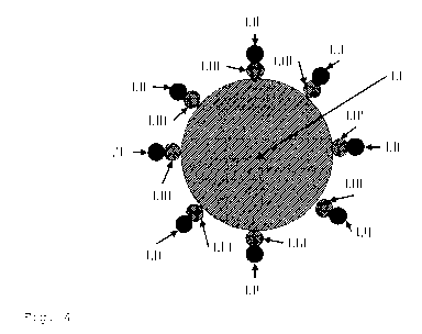
Figure 4 shows a schematic illustration of a single metal
oxide particle (I.I) as shown in figure 3, with the metal
salt (cation 1.111 and anion 1.11) adsorbed on its surface.
Without being bound to theory, it is believed that the
positively charged metal cation (I.III) will physisorb onto
the negatively charged particle surface (I.I) and that the
negatively charged anion (I.II) is present bound to the
cation (as shown). In case the metal oxide particle is
dispersed in a liquid phase, e.g. the inventive
suspensions, the anion may also be spatially separated (not
shown).
Figure 5 shows atomic force micrographs (10 x 10
micrometers) of films obtained according to example 5,
left: this invention, right according to the prior art.
CA 02974044 2017-07-17
WO 2016/128133
PCT/EP2016/000220
12
In a first aspect, the invention relates to an electronic
device, particularly selected from the group of
optoelectronic devices, wherein said device comprises a
substrate and a multitude of layers, wherein at least one
of said layers is a buffer layer, wherein said buffer layer
comprises metal oxide nanoparticles, wherein on the surface
of said nanoparticles metal salts as described herein are
physisorbed.
In more general terms, the invention relates to buffer
layers in an electronic device, said buffer layers having
a specific and beneficial composition containing metal
oxide nanoparticles as described. It was found that the
present inventive buffer layers provide beneficial
properties to the electronic devices because: (i) no post-
treatment (e.g. plasma cleaning or annealing temperatures
> 15000) is required allowing an all-solution manufacturing
process; (ii) only a very small amount of dispersing agent
is needed thus leading to a high performance of the
electronic devices.
This aspect of the invention shall be explained in further
detail below.
The terms electronic devices and optoelectronic devices
are defined above.
In one embodiment, the device is selected from the group
of organic solar cells (OPV, including perovskite type
solar cells), organic light emitting diodes (OLED), organic
photodetectors and quantum dot LED (QLED); particularly
OPV and OLED, very particularly OPV.
In a further embodiment, the invention relates to an OPV
device with tandem architecture.
In a further embodiment, the invention relates to an OPV
device with tandem architecture whereby an inventive layer
CA 02974044 2017-07-17
WO 2016/128133
PCT/EP2016/000220
13
of the present invention is part of the recombination
layer.
In one embodiment, the buffer layer is selected from the
group consisting of hole transport (HTL), hole injection
(HIL), hole extraction (HEL), electron transport (ETL),
electron injection (EIL) and electron extraction (EEL)
layers, preferably HTL, HIL, HEL.
In one embodiment, the buffer layer is located on top of
hydrophobic or hydrophilic organic materials, preferably
PEDOT:PSS, photoactive polymers (absorbers or emitters) or
photoactive small molecules (absorbers or emitters).
In one further embodiment, the buffer layer is located on
top of a hydrophilic inorganic material, preferably ITO or
silver (including a vacuum deposited dense Ag layer or a
solution processed porous Ag nanowire layer).
In one embodiment, the top and/or bottom electrode of the
device is a silver, a copper or a nickel electrode,
particularly a Ag-, Cu- or Ni- nano wire electrode. The
nano wires of such electrodes can be embedded in the
hydrophilic or hydrophobic organic materials as defined
above, particularly in PEDOT:PSS.
In one embodiment, the top and bottom electrodes are both
made from metal nanowires. This embodiment provides
transparent or semitransparent electronic devices. The
nano wires of such electrodes can be embedded in the
hydrophilic or hydrophobic organic materials as defined
above, particularly in PEDOT:PSS.
In one embodiment, the top and/or bottom electrode is pure
PEDOT:PSS.
In one further embodiment, the top and/or bottom electrode
is a combination of PEDOT:PSS with a regular metal
collector grid (such as an Ag-, Cu- or Ni- collector grid).
CA 02974044 2017-07-17
WO 2016/128133
PCT/EP2016/000220
14
Metal oxide nanoparticles: The term metal oxide
nanoparticles is defined above.
In one embodiment, the nanoparticles are selected from the
group consisting of pure metal oxides, preferably NizOy
(including NiO), ZnO y (including ZnO), Tiz0y, Wz0y, Vz0y,
Moz0y, Yz0y, Ta10y, Cuz0y, Zr20y, Sn20y, InzOy and Nb20y. A
particularly preferred pure metal oxide is NiO. A further
particularly preferred pure metal oxide is ZnO. A further
particularly preferred pure metal oxide is CrzOy.
In one embodiment, the nanoparticles are selected from the
group consisting of mixed metal oxides, preferably zinc
containing mixed metal oxides, most preferably indium
gallium zinc oxide (IGZO), indium zinc oxide (IZO), zinc
tin oxide (ZnSn03). A further preferred mixed metal oxide
is BaSn03.
In one embodiment, the nanoparticles are selected from the
group consisting of doped metal oxides, particularly doped
Ni20y, Znz0y, Ti20y, W20y, Vz0y, Moz0y, Yz0y, Taz0y, Cuz0y, Zrz0y,
Sn10y, InzOy and Nbz0y, most preferably Niz0y, ZnO, Tiz0y,
InzOy and Snz0y. Suitable dopants and amounts of dopants are
known in the field. The term doped metal oxide relates to
compositions of MO x where Metal (M) is substituted by one
or more metals (="dopants"). The dopant atoms are
incorporated into the My0x crystal lattice either
substitutionally or interstitially forming a homogeneous
single-phase (a "solid solution"). Specific examples
include ITO (indium tin oxide; typical 90% In203: 10% Sn02),
ATO (antimony doped tin oxide; typical 90% Sn02: 10% Sb203)
and AZO (aluminum doped zinc oxide; typical 97% ZnO : 3%
A1203). In the context of the present invention, separated
multiphase systems (e.g. MO x + Fe203) are not considered
doped oxides. Doping of oxides can enable the fine tuning
of the properties of the inventive thin films, such as
CA 02974044 2017-07-17
WO 2016/128133
PCT/EP2016/000220
electrical conductivity, work function and / or optical
absorbance.
In a preferred embodiment said metal oxides are doped with
0.001 - 30 wt%, preferably 0.01 - 15 wt%, most preferably
5 0.1 - 10 wt% (with respect to the metal), by one or more
metals.
In a preferred embodiment, said dopant atoms are selected
from the group consisting of transition metals, alkaline
metals and earth-alkaline metals.
Metal Salt: According to the present invention, metal salts
are physisorbed on the surface of the nanoparticles. The
term physisorbed is defined above. It is apparent that
physisorption only takes place on the surface of the
nanoparticles. Without being bound to theory, it is
believed the metal salts act as a dispersant. In the
context of the present inventions, metal salts are
therefore termed dispersants. The amount of metal salts
physisorbed on the surface may vary over a broad range.
Suitable amount of metal salts are in the range of 0.02-6
mol%, preferably 0.1-4 mol%, most preferably 0.2-2 mol%
molar fraction of metal salt cation to metal atoms/ions in
the nanoparticle. These amounts depend on the specific
surface exhibited by the nanoparticles and may be
determined by the skilled person.
In one embodiment, the metal salt is of formula (I)
mza+Ryb- (I)
wherein
M represents a metal cation,
R represents the corresponding salt anion,
a is 2, 3, 4 or 5, preferably 2 or 3
b is 1, 2 or 3, preferably 1 or 2
z is 1, or a real number below 1 but excluding 0,
y is z*a/b
CA 02974044 2017-07-17
WO 2016/128133
PCT/EP2016/000220
16
The metal cation (M) is preferably Zn, Al, Y, Pb, Bi, Cu,
Ni, Co, Fe, Mn, Cr, V, Ti, La, Mg, Ca, Sr or Ba and is most
preferably Zn, Al or Y.
The salt ion (R) is preferably acetate, formiate, citrate,
oxalate, nitrate or halogenide and is most preferably
acetate or nitrate.
In a preferred embodiment, the metal atom/ion of the
dispersant salt differs from the metal atom/ion which is
present in the major concentration in the nanoparticle.
In a preferred embodiment, the metal atom/ion of the
dispersant salt differs from any metal atom/ion present in
the nanoparticle which is present in a concentration larger
than 0.1 wt% (relative to the nanoparticle composition)
The metal salts described herein are commercial items. Such
metal salts may be made by any method known in the art.
In one embodiment, the invention provides a buffer layer
with a composition as described herein wherein said layer
consists of metal oxide nanoparticles and a dispersant as
described herein.
In one embodiment, said metal oxide nanoparticles are
coated with one type of dispersant as defined herein.
In one alternative embodiment, said metal oxide
nanoparticles are coated with two or more types of
dispersant as defined herein. In this embodiment, either
an individual nanoparticle is coated with said two or more
types of dispersant or a first group on nanoparticles is
coated with a first dispersant, a second group of nano-
particles is coated with a second dispersant and so on.
In a further embodiment, the invention provides a buffer
layer with the following composition: 70 - 99.9 wt%,
preferably 80 - 99.5 wt%, most preferably 90 - 99 wt% metal
CA 02974044 2017-07-17
WO 2016/128133
PCT/EP2016/000220
17
oxide nanoparticles and 0.1-30 wt% metal salt, preferably
0.5-20 wt% metal salt, most preferably 1-10 wt% metal salt.
These ratios are preferably measured by secondary ion mass
spectrometry (SIMS) techniques (eg. TOF-SIMS).
In an advantageous embodiment, the invention provides a
buffer layer as described herein containing 70 - 99.9 wt%,
preferably 80 - 99.5 wt%, most preferably 90 - 99 wt% NiO
nanoparticles and 0.1-30 wt%, preferably 0.5-20 wt%, most
preferably 1-10 wt% dispersant.
In an advantageous embodiment, the invention provides a
buffer layer as described herein containing 70 - 99.9 wt%,
preferably 80 - 99.5 wt%, most preferably 90 - 99 wt% ZnO
nanoparticles and 0.1-30 wt%, preferably 0.5-20 wt%, most
preferably 1-10 wt% dispersant.
In an advantageous embodiment, the invention provides a
buffer layer as described herein containing 70 - 99.9 wt%,
preferably 80 - 99.5 wt%, most preferably 90 - 99 wt% AZO
nanoparticles and 0.1-30 wt%, preferably 0.5-20 wt%, most
preferably 1-10 wt% dispersant.
In an advantageous embodiment, the invention provides
buffer layers as described herein comprising:
Ni0 nanoparticles and Y(NO3)3 salt of formula (I); or
ZnO nanoparticles and Y(NO3)3 salt of formula (I); or
AZO nanoparticles and Y(NO3)3 salt of formula (I).
In a further embodiment, the invention provides an
electronic device as described herein wherein said buffer
layers have a film thickness of 3 - 1000 nm, preferably 10
- 500 nm. In one embodiment, monolayers, typically 3-30 nm
thick are also envisaged. Thickness may be determined by
profilometry, atomic force microscopy or electron
microscopy.
In a further embodiment, the invention provides an
optoelectronic device as described herein wherein said
CA 02974044 2017-07-17
WO 2016/128133
PCT/EP2016/000220
18
oxide nanoparticles have a primary particle diameter of 1
- 100 nm, preferably 3 - 50nm (measured by nitrogen
absorption, X-Ray diffraction or transmission electron
microscopy).
In a further embodiment, the invention provides an
electronic device as described herein wherein said oxide
nanoparticles exhibit a bimodal or multimodal size
distribution. It is believed that bimodal or multimodal
size distributions result in higher particle packing
densities, thus resulting in lower layer porosity.
In a further embodiment, the invention provides an
electronic device as described herein wherein said buffer
layers have a mean surface roughness below 100 nm,
especially below 30 nm (determined by electron microscopy,
atomic force microscopy or profilometry).
In a further embodiment, the invention provides an
electronic device as described herein wherein said buffer
layer comprises, in addition to the nanoparticles as
described herein, scattering particles. Accordingly,
buffer layers of the present invention may additionally
comprise scattering particles, typically having a
refractive index of > 2.3 and being comparatively large,
typically with a particle size of 100 - 500 nm. The presence
of such scattering particles provides for controlled Haze
to an electronically functional buffer layer. The use of
such buffer layers with light scattering properties (Haze)
is for light extraction (light outcoupling) in OLED devices
or for light incoupling in solar cells, which enhances the
efficiency of either device (more light gets into solar
cell or more light is extracted from an OLED). Typical
compositions of scattering particles are BaTiO3, SrTiO3,
Ti02. Typical concentrations of scattering particles in
the dry buffer layer range from 5 - 50 wt%.
CA 02974044 2017-07-17
WO 2016/128133
PCT/EP2016/000220
19
In a further embodiment, the invention provides an
electronic device as described herein wherein said buffer
layer has an electrical conductivity of 10-8-103 S/cm,
preferably 10-6-102, most preferably 10-3-10 (determined by
4-point conductivity measurement).
In a more specific embodiment, the invention provides an
electronic device as described herein wherein said buffer
layer comprises scattering particles and has an electrical
conductivity of 10-1-103 S/cm.
In a further embodiment, the invention relates to an OLED
wherein the ETL or EIL (i) is obtained by a method as
described herein or (ii) consists of metal oxide
nanoparticles coated with a dispersant as described herein.
In a further embodiment, the invention relates to an OLED
wherein the HTL or HIL (i) is obtained by a method as
described herein or (ii) consists of metal oxide
nanoparticles coated with a dispersant as described herein.
In a further embodiment, the invention relates to an OLED
wherein the device stack comprises the sequence electrode
/ HIL / HTL / active layer / ETL / EIL / electrode.
In a further embodiment, the invention relates to an OLED
wherein the ETL layer consists of a monolayer of
nanoparticles coated with a dispersant as described herein.
In a further embodiment, the invention relates to an
organic solar cell (OPV) wherein the ETL (i) is obtained
by a method as described herein or (ii) consists of metal
oxide nanoparticles coated with a dispersant as described
herein.
In a further embodiment, the invention relates to a
perovskite solar cell wherein the HTL (i) is obtained by a
method as described herein or (ii) consists of metal oxide
nanoparticles coated with a dispersant as described herein.
CA 02974044 2017-07-17
WO 2016/128133
PCT/EP2016/000220
In a further embodiment, the invention relates to an
organic photodetector wherein the ETL (i) is obtained by a
method as described herein or (ii) consists of metal oxide
5
nanoparticles coated with a dispersant as described herein.
In a further embodiment, the invention relates to an
electronic device wherein the ETL (i) is obtained by a
method as described herein or (ii) consists of metal oxide
10
nanoparticles coated with at least one type of a dispersant
as described herein.
Use: In a further embodiment, the invention relates to the
use of metal oxide nanoparticles coated with metal salts
15 as
described herein for manufacturing an electronic device
as described herein, particularly selected from the group
of OLEDs, OPVs, perovskite type solar cells,
photodetectorsand QLEDs.
20 In a second aspect, the invention relates to an
intermediate good ("a component") comprising a sheet-like
substrate coated with a multitude of layers wherein at
least one of said layers, preferably a buffer layer,
comprises nanoparticles with physisorbed metal salts as
defined in the first aspect of the invention.
This aspect of the invention shall be explained in further
detail below.
Intermediate good ("component"): As outlined above, there
is a need for manufacturing organic electronics by solution
based processes. Accordingly, a component is manufactured
by suitable solution based processes, such as coating or
printing; the thus obtained material is then finished to
obtain the final device (the organic electronic).
In one embodiment, the invention provides a component as
defined herein, wherein said layers have the sequence
CA 02974044 2017-07-17
WO 2016/128133
PCT/EP2016/000220
21
substrate / electrode / HTL / active layer / ETL /
electrode. ("normal architecture").
In one further embodiment, the invention provides a
component as defined herein, wherein said layers have the
sequence substrate / electrode / ETL / active layer / HTL
/ electrode. ("inverted architecture").
In one further embodiment, the invention provides a
component as defined herein, wherein said layers comprise
the sequence electrode / ETL / active layer / HTL. This
intermediate may also be the basis of a tandem cell.
In one further embodiment, the invention provides a
component as defined herein, wherein said layers comprise
the sequence electrode / HTL / active layer / ETL. This
intermediate may also be the basis of a tandem cell.
In one further embodiment, the invention provides a
component as defined herein, wherein said layers comprise
the sequence electrode / HTL / ETL / electrode.
In one further embodiment, the invention provides a
component as defined herein, wherein said layers comprise
the sequence electrode / ETL / HTL / electrode.
In one further embodiment, the invention provides a
component as defined herein, wherein said layers have the
sequences:
(a) Transparent electrode/ HTL /active layer / ETL
(b) Non-transparent electrode/ HTL /active layer/ ETL
(c) Transparent electrode /ETL / active layer / HTL
(d) Non-transparent electrode/ ETL /active layer /HTL,
whereby the transparent electrode is selected from the
group consisting of: PEDOT:PSS, Metal nanowires (including
Silver nanowires, Copper nanowires, Nickel nanowires),
metal grids, Graphene, Carbon nanotubes and ITO; and
whereby the non-transparent electrode is selected from the
group consisting of dense silver, dense aluminum, dense
CA 02974044 2017-07-17
WO 2016/128133
PCT/EP2016/000220
22
copper, dense gold, thick (opaque) carbon nanotube layer
and thick (opaque) graphene-based layer.
In one further embodiment, the invention provides a
component as defined herein, wherein no additional layer
is present.
In one further embodiment, the invention a component as
defined herein, wherein the buffer layer has a thickness
between 3-1000 nm, preferably 10-500 nm.
In one further embodiment, the invention provides a
component as defined herein, wherein the buffer layer has
a mean surface roughness below 30 nm.
In one further embodiment, the invention provides a
component as defined herein, wherein the buffer layer has
a metal salt content in the range of 0.1-30 wt%, preferably
0.5-20 wt%, most preferably 1-10 wt%.
In one further embodiment, the invention provides a
component as defined herein, the substrate is as defined
above.
Use: In one further embodiment, the invention provides for
the use of metal oxide nanoparticles comprising physisorbed
metal salts as described herein for manufacturing of an
intermediate good ("component") as defined herein.
In a third aspect, the invention relates to a composition
in the form of a suspension, said composition containing
metal oxide nanoparticles, solvent(s) and a dispersant
selected from the group of metal salts as described herein.
The use of such suspensions for manufacturing thin films,
such as buffer layers, is novel and subject of the present
invention. Further, certain suspensions are novel and thus
also subject of the present invention. This aspect of the
invention shall be explained in further detail below.
CA 02974044 2017-07-17
WO 2016/128133
PCT/EP2016/000220
23
New uses: The invention provides for the use of a
suspension, comprising metal oxide nanoparticles coated
with a dispersant as described herein and a polar solvent,
(i) for manufacturing of an intermediate good ("component")
as defined herein or (ii) for manufacturing an electronic
device as described herein; said device particularly
selected from the group of OLEDs, OPVs, perovskite type
solar cells, photodetectors and QLEDs.
For these uses, suitable suspensions (II) comprise 0.2 -
50 wt-%, preferably 1 - 20 wt% nanoparticles (1) as
described herein; 0.005 - 10 wt-%, preferably 0.01 - 5 wt-
% metal salt (2) as described herein; 20 - 99.795 wt-%,
preferably 30 - 98.99 wt-% solvent (4) as defined above,
preferably water, dimethyl sulfoxide, dimethyl formamide,
dimethyl acetamide, methanol, acetonitrile, ethylene
glycol, propylene carbonate, acetone, 2,2,3,3-tetrafluoro-
1-propanol, most preferably methanol, acetonitrile,
2,2,3,3-tetrafluoro-l-propanol and water.
New Suspensions: Further, certain of the above defined
suspensions are novel and thus subject of the present
invention. The term suspension is defined above.
In one embodiment, the invention provides for a composition
in the form of a suspension comprising (i) nanoparticles
selected from the group of metal oxide nanoparticles and
(ii) one or more solvents and (iii) one or more dispersants
from the group of metal salts as described herein.
Nanoparticles: The amount of nanoparticles in the inventive
composition may - depending on the intended use - vary over
a broad range, but typically is in the range of 0.2 - 50
wt% (preferably 1 - 20 wt%) of the composition.
Advantageously, the nanoparticles in suspension have a
hydrodynamic size D90 of less than 100 nm (measured by
dynamic light scattering or centrifugal sedimentation
techniques).
CA 02974044 2017-07-17
WO 2016/128133
PCT/EP2016/000220
24
Advantageously, the nanoparticles are synthesized by a gas
phase pyrolysis process, preferably flame spray synthesis.
Dispersants: Suitable dispersants are discussed above and
particularly include metal salts of formula (I). Without
being bound to theory, it is believed that the dispersants
in the inventive suspension are partly physisorbed on the
nanoparticles surface and partly dissolved in the solvent.
Solvents: Suitable solvents include polar solvents as
discussed above, and are preferably selected from the group
consisting of water, dimethyl sulfoxide, dimethyl
formamide, dimethyl acetamide, methanol, acetonitrile,
ethylene glycol, propylene carbonate, acetone, and
2,2,3,3-tetrafluoro-l-propanol. Particularly preferred are
polar solvents selected from the group consisting of
methanol, acetonitrile, 2,2,3,3-tetrafluoro-l-propanol and
water. It is understood that the term solvent also
comprises combinations of the named above solvents.
In a forth aspect, the invention relates to the
manufacturing of the inventive compositions, intermediate
goods and devices disclosed herein and to inventive
compositions, intermediate goods and devices obtained
according to these methods. This aspect of the invention
shall be explained in further detail below.
Manufacturing of suspensions: The manufacturing of
suspensions is a known procedure. The coating of
nanoparticles is also a known procedure. These procedures
may be applied to the starting materials of the inventive
suspensions.
In one embodiment, solvent and nanoparticles are combined,
for example by mixing, ultrasonication or ball milling. To
the obtained initial suspension, the dispersants (i.e.
metal salts) are added. Coating takes place at room
temperature or upon heating and mixing.
CA 02974044 2017-07-17
WO 2016/128133
PCT/EP2016/000220
In one alternative embodiment, solvent and dispersants
(i.e. metal salts) are combined, for example by mixing. To
the obtained initial solution, the nanoparticles are added.
Coating takes place at room temperature or upon heating
5 and mixing.
Manufacturing of intermediate goods: The intermediate
goods according to the present invention may be obtained
by solution processes. This is considered a significant
10 advantage, as it enables manufacturing of all layers by
simple technologies applicable to large areas and
continuous processing.
In one embodiment, the invention provides for a method for
manufacturing an intermediate good as defined herein,
15 wherein the buffer layer is manufactured comprising the
steps of (a) applying a suspension on a substrate or coated
substrate, said suspension comprising metal oxide
nanoparticles coated with a dispersant and a solvent and
removing the solvent from said composition and (b) removing
20 the solvent from the obtained thin film and (c) optionally
treating the dry layer at elevated temperature.
Step (a) Application of a suspension: Many processes are
known to apply a liquid composition to a substrate to
result in a wet thin film; a person skilled in the art is
25 in a position to appropriately select. Suitable are, for
example coating, particularly roll-to-roll-, slot-die-,
spray-, ultrasonic spray-, dip-, reel-to-reel-, blade-
coating; or by printing, particularly ink-jet-, pad-,
offset-, gravure-, screen-, intaglio-, sheet-to-sheet-
printing. Such processes are generally considered
advantageous for large scale production, when compared to
vacuum-based processes. Depending on the composition used
in step (a), this step may be repeated (i.e. may be
performed multiple times). This embodiment is considered
advantageous in order to fine tune the final film
thickness.
Step (b) Drying and film formation: Many processes are
known to remove a liquid from a wet thin film of a coated
CA 02974044 2017-07-17
WO 2016/128133
PCT/EP2016/000220
26
substrate; a person skilled in the art is in a position to
appropriately select. Suitable are, for example drying at
room temperature or elevated temperature. Drying may take
place in air, in a protecting gas, such as nitrogen or
argon. Especially suited are gases with low humidity
content (e.g. nitrogen, dry air, argon).
Step (c): Temperature cleaning step: A cleaning step in
the form of a temperature annealing can optionally be
conducted at temperatures below 150 C. In an advantageous
embodiment, the dried nanoparticle film in step (c) is
annealed at 80 C - 150 C in air or in a protecting gas.
In an advantageous embodiment, all layers of the
intermediate good are manufactured by coating or printing.
Manufacturing of devices: The manufacturing of devices
starting from the above described intermediate goods is
known per se, but not yet applied to the specific
intermediate goods of the present invention.
Accordingly, the invention provides a method for
manufacturing an electronic device as defined herein
comprising the steps of (a) providing an intermediate good
as defined herein, (b) contacting the layers of said good
with an electrical circuit, (d) finishing the obtained
product.
Product by process: Due to the novel buffer layer obtained
according to the inventive method, the electronic devices
and intermediate goods are also novel. Due to the
outstanding stability and performance obtained according
to the inventive method, the suspensions are also novel.
The invention thus provides for a suspension obtained by a
method comprising the step of combining metal oxide
nanoparticles, dispersant(s) and solvent(s).
The invention thus provides for an intermediate good,
obtained by a method comprising the steps of applying a
suspension on a substrate or coated substrate, said
suspension comprising (i) metal oxide nanoparticles coated
with a dispersant and (ii) a solvent and removing the
CA 02974044 2017-07-17
WO 2016/128133
PCT/EP2016/000220
27
solvent from said composition and optionally treating the
dry layer at elevated temperature.
The invention thus provides an electronic device, obtained
by a method comprising the steps of providing an
intermediate good as defined herein, contacting the layers
with an electrical circuit, finishing the obtained product.
To further illustrate the invention, the following examples
are provided. These examples are provided with no intent
to limit the scope of the invention.
Example 1: Nickel oxide (NiO) nanoparticles were
synthesized by flame spray synthesis. For the preparation
of the precursor, 269.2g Ni-acetate tetrahydrate (Sigma
Aldrich) was added to 1080g 2-ethylhexanoic acid (Aldrich)
and dissolved by heating the mixture for 1 hour at 150 C.
To the obtained solution, 540g tetrahydrofuran (Sigma
Aldrich) was added and well mixed. The precursor then was
fed (7 ml min-1, HNP Mikrosysteme, micro annular gear pump
mzr-2900) to a spray nozzle, dispersed by oxygen (15 I min
1, PanGas tech.) and ignited by a premixed methane-oxygen
flame (CH4: 1.2 1 min-1, 02: 2.2 1 min-1). The off-gas was
filtered through a glass fiber filter (Schleicher &
Schuell) by a vacuum pump (Busch, Seco SV10400V) at about
20 m3 h-1. The obtained oxide nanopowder was collected from
the glass fiber filter.
The mean crystallite size was measured with a Rigaku
MiniFlex 600, an SC-70 Detector, measured from 10 to 70
at 0.01 step size by using the Scherrer equation. The mean
crystallite size of the SrTiO3 particles was 10 nm.
For the preparation of suspensions, 5 wt% of NiO nanopowder
(as described above), 0.1 wt% of Yttrium(III) nitrate
hexahydrate (Aldrich) and 94.9 wt% methanol (Merck) were
dispersed by ball-milling for 1 hour. The finally prepared
suspension is black and stable for more than 1 week (no
supernatant visible after 1 week).
CA 02974044 2017-07-17
WO 2016/128133
PCT/EP2016/000220
28
For the device fabrication the patterned ITO substrates
were subsequently ultrasonic cleaned with acetone and
isopropanol for 10 minutes each. On cleaned ITO substrate,
a dense and smooth layer of the above described NiO-
suspension was deposited by spin coater at a speed of 4000
and followed by annealing at 140 C for 15 minutes in air
leading to a dry film thickness of -30 nm. The following
steps were conducted in a nitrogen glovebox: PbI2 and
CH3NH3I mixed with mole ratio of 1:1 with a concentration
of - 40% were stirred in a mixture of dimethylformamide
and dimethyl sulfoxide (2:1 v/v) at 60 C for 12 h. The as-
prepared perovskite precursor solution was filtered using
0.45 pm PTFE syringe filter and coated onto the ITO/NiO
substrate at a speed of 4,000 r.p.m for 35 s. During the
last 5 s of the whole spinning process, the substrate
(around 2.5 cm x 2.5 cm) was treated with chlorobenzene
(CB) drop-casting. The substrate was dried on a hot plate
at 100 C for 10 min. A 2wt % PCBM solution in CB was spin-
coated on the ITO/NiO/MAPbI3 substrate at 1200 r.p.m for
s. Finally, a 100-nm-thick Ag counter electrode was
deposited through a shadow mask by thermal evaporation.
Device characterizations: J-V characteristics of all the
25 devices were measured using a source measurement unit from
BoTest. Illumination was provided by a Newport SollA solar
simulator with AM1.5G spectrum and light intensity of
100mWcm-2, which was determined by a calibrated crystalline
Si-cell. During device characterization, a shadow mask with
30 an opening of 10.4 mm2 was used. The EQE spectra were
recorded with by an Enli Technology (Taiwan) EQE
measurement system (QE-R), and the light intensity at each
wavelength was calibrated with a standard single-crystal
Si photovoltaic cell. The cell prepared as described above
reached a photoconversion efficiency (POE) of 13.98% with
a short circuit current of 19.22 mA/cm2, a open circuit
voltage of 1.10 V and a fill factor of 66.2%.
CA 02974044 2017-07-17
WO 2016/128133
PCT/EP2016/000220
29
Example 2: 5 wt% of the NiO-nanopowder from experiment 1,
0.5wt% Diethylphosphato-ethyl-triethoxysilane (ABCR) and
94.5 wt% of isopropanol (BASF) were dispersed by ball-
milling for 1 hour. The finally prepared suspension is
black and stable for more than 1 week (no supernatant
visible after 1 week).
Devices produced as described in experiment I reached a
photoconversion efficiency (POE) of 1.60% with a short
circuit current of 3.30 mA/cm2, a open circuit voltage of
1.08 V and a fill factor of 44.9%.
Example 3: A variety of combinations of different types of
nanopowders, metal salts and solvents were used for
preparing suspensions. 5wt% of nanopowder, 0.25 wt% of
metal salt and 94.75 wt% of solvent were dispersed by ball-
milling for 15 minutes. The nanopowders were either
prepared similarly to experiment 1 or were commercially
available. The metal salts as well as solvents were all
commercially available. The hereby prepared suspensions
were evaluated after 3 days. The suspensions were
considered instable if there was a phase separation such
that there was a clear supernatant of 30% or more in height
regarding to the total suspension filling height and were
considered stable if less than 30% in height. The results
are shown in the following table:
Nanopowder Metal Salt (I) Solvent
Result
(metal oxide) (disperant)
Yttrium(III) nitrate
TiO2 Methanol
stable
hexahydrate
Yttrium(III) nitrate
Zr02 Methanol
stable
hexahydrate
Yttrium(III) nitrate
Y203 Methanol
stable
hexahydrate
Yttrium(III) nitrate
Nb205 Methanol
stable
hexahydrate
Yttrium(III) nitrate
Ta205 Methanol
stable
hexahydrate
Calcium(II) acetate
NiO Methanol
stable
hydrate
CA 02974044 2017-07-17
WO 2016/128133
PCT/EP2016/000220
Lanthanum (III)
NiO Methanol stable
nitrate hexahydrate
NiO Aluminum chloride Methanol stable
Yttrium(III) nitrate
NiO Water stable
hexahydrate
Yttrium(III) nitrate
Ni0 Dimethyl sulfoxide stable
hexahydrate
Yttrium(III) nitrate
NiO 1,2-Propanediol stable
hexahydrate
Yttrium(III) nitrate
NiO Ethanol stable
hexahydrate
Yttrium(III) nitrate
NiO Ethylene glycol stable
hexahydrate
Aluminum nitrate
NiO Methanol stable
nonahydrate
2,2,2,3-Tetrafluoro-1-
ZnO Zinc acetate stable
propanol
2,2,2,3-Tetrafluoro-1-
AZO Zinc acetate stable
propanol
Y203 Zinc acetate Methanol stable
Yttrium(III) acetate
Y203 Methanol stable
hydrate
Example 4: 5 wt% of the NiO-nanopowder from experiment 1,
various amounts of Yttrium(III) nitrate hexahydrate
(Aldrich) and methanol (Merck) were dispersed by ball-
5 milling for 15 minutes. Stability was evaluated similar to
Example 3. The following results were found: Suspension
containing 0.005wt% and 0.025wt% of Yttrium(III) nitrate
hexahydrate were found to be not stable (corresponding to
0.1 and 0.5 wt%, respectively), while a suspension
10 containing 0.05wt% or more of Yttrium(III) nitrate
hexahydrate (corresponding to 1 wt%) were found to be
stable.
Example 5: Comparative example between this invention and
15 Kim et al (Nanoscale Research Letters 2014, 9, 323).
Experimental:
5 wt% nanoparticles (Zn0; synthesized by flame spray
pyrolysis) are dispersed in the solvent (ethanol or
20 methanol) in the presence of 5 wt% dispersant (metal salt:
Cs2CO3 (according to Kim) or YNO3x6H20 (this invention),
CA 02974044 2017-07-17
WO 2016/128133
PCT/EP2016/000220
31
total dispersant concentration:0.25 %). The suspensions
are prepared in analogy to example 4. Film coating was
effected with a spin coater @5000rpm. Paricle size was
determined with LUMISIZER by dissolution to 0.5 wt% ZnO in
methanol. The results are provided below and in fig.5.
Results:
Table 1: Solvent ethanol
Y(NO3)3x6H20 Cs2CO3
Dispersion
appearance of very turbid very turbid
dispersion not stable: not stable:
sedimentation within sedimentation within
5min 5min
Table 2: Solvent methanol
Y(NO3)3x6H20 Cs2CO3
This invention for comparison
Dispersion
appearance of stable, no sedimentation not stable, sedi-
dispersion: for at least 3 hours mentation within 5min
particle size: 80 nm 2049 nm
Film
appearance of transparent, homogeneous hazy, inhomogeneous
film Coating: films after coating films after coating
Film roughness: Ra = 5.6nm Ra = 37.8 nm
average hydrodynamic particle size in dispersion (D50; nm)
Conclusion:
The data provided in this example convincingly show that
nanoparticles coated with Cs2CO3 [corresponding to metal
salts of formula (I) where a=1] are unsuited to prepare
stable suspensions and also result in films with high
roughness.
The data provided in this example further show that the
same nanoparticles coated with Y(NO3)3 [corresponding to
metal salts of formula (I) where a=3] are suited to prepare
stable suspensions with polar solvents and also result in
films with low roughness.
Optoelectronic devices comprising inventive nanoparticles
are superior when compared to devices comprising known
nanoparticles.