Note: Descriptions are shown in the official language in which they were submitted.
- 1 -
MINIATURIZED OCT PACKAGE AND ASSEMBLY THEREOF
BACKGROUND
Field
Embodiments of the invention relate to designs of a miniaturized OCT system.
Background
Optical coherence tomography (OCT) is an imaging technique that is widely used
in many
fields to provide depth-revolved imaging of various samples. The technique has
found
widespread use in the medical field where OCT data is used on skin and tissue
to help
diagnose various ailments as well as provide enhanced visual feedback to
medical
practitioners. Miniaturization of an OCT system is difficult due to the number
of components
required and the high coupling sensitivities between optical elements.
BRIEF SUMMARY
In the embodiments presented herein, designs of an integrated, miniaturized
OCT system, and
methods for fabricating such a system, are presented.
In an embodiment, a chip package includes a housing, one or more electrical
connections
coupled to an exterior of the housing, a photonic integrated circuit, and a
scanning unit. Both
the photonic integrated circuit and the scanning unit are disposed within the
housing. The
photonic integrated circuit has at least one waveguide designed to guide a
beam of light. The
scanning unit is designed to laterally scan the beam of light across a focal
plane outside of the
housing. The scanning unit is aligned with the photonic integrated circuit
such that the beam
of light is coupled between the photonic integrated circuit and the scanning
unit.
In another embodiment, a method includes attaching a heat sink to one side of
a photonic
integrated circuit, and attaching an opposite side of the heat sink to a base
of a package. The
CA 2975945 2017-12-20
-2-
method further includes attaching a photo detector to the heat sink. The
method also includes
attaching a fiber mount to the heat sink. The fiber mount holds, and aids in
the alignment of,
optical fibers within the package. The method also includes attaching a
scanning unit to the
base of the package, where the attaching of the scanning unit, the attaching
of the fiber mount,
and the attaching of the photo detector align the photonic integrated circuit,
photo detector,
fiber mount, and scanning unit so as to maximize a coupling efficiency of a
beam of light
traveling between the photonic integrated circuit, photo detector, fiber
mount, and scanning
unit.
BRIEF DESCRIPTION OF THE DRAWINGS/FIGURES
The accompanying drawings form a part of the
specification, illustrate embodiments of the present invention and, together
with the
description, further serve to explain the principles of the invention and to
enable a person
skilled in the pertinent art to make and use the invention.
FIG. 1 illustrates a chip package, according to an embodiment.
FIG. 2 illustrates example dimensions of a chip package.
FIG. 3 illustrates example electro-optical characteristics of a photo diode
array.
FIG. 4 illustrates a heat spreader element, according to an embodiment.
FIG. 5 illustrates a fiber mount structure, according to an embodiment.
FIG. 6 illustrates an example spectral response of a polarizer.
FIG. 7 illustrates a micro-lens array, according to an embodiment.
FIG. 8 illustrates inputs and outputs of a photonic integrated circuit,
according to an
embodiment.
FIG. 9 illustrates a scanner device, according to an embodiment.
FIG. 10 illustrates an example rib waveguide and corresponding beam profile
within the
waveguide.
FIG. 11 illustrates an example beam profile through an optical fiber.
FIG. 12 illustrates an example coupling loss to a waveguide.
FIG. 13 illustrates example alignment tolerances between light guiding
mediums.
FIG. 14 illustrates an example simulation of light focusing.
FIG. 15 illustrates example fiber alignment tolerances.
CA 2975945 2017-12-20
CA 02975945 2017-08-04
WO 2016/124762 PCT/EP2016/052549
-3-
FIG. 16 illustrates simulated coupling losses into a waveguide, according to
an embodiment.
FIGs. 17A and 17B illustrate simulated coupling efficiencies, according to
some
embodiments.
FIG. 18 illustrates simulated spatial tolerances based on separation distance,
according to an
embodiment.
FIG. 19 illustrates a stacked heat sink design, according to an embodiment.
FIG. 20 illustrates balanced sample and reference arms of an interferometer,
according to an
embodiment.
FIG. 21 illustrates an example assembly of a circuit board and photodiode
array, according to
an embodiment.
FIG. 22 illustrates an example assembly of a scanning unit, according to an
embodiment.
FIG. 23 illustrates an example wire bonding scheme.
FIG. 24 illustrates an example assembly for placing an element within a
package.
FIG. 25 illustrates another view of the example assembly for placing an
element within a
package.
FIG. 26 illustrates a mounting bracket, according to an embodiment.
FIG. 27 illustrates the mounting bracket with the example assembly for placing
an element
within a package, according to an embodiment.
FIG. 28 illustrates another view of the mounting bracket with the example
assembly for
placing an element within a package, according to an embodiment.
FIGs. 29 - 31 illustrate various stages of assembling and aligning a lens
array, according to an
embodiment.
FIGs. 32 and 33 illustrate the alignment of a fiber mount to waveguide of a
photoninc
integrated circuit, according to an embodiment.
FIG. 34 illustrates a method, according to an embodiment.
Embodiments of the present invention will be described with reference to the
accompanying
drawings. Although some of the drawings may include specific measurements,
dimensions,
and/or photographs of prototype parts, such specifics are not to be considered
limiting to the
scope of the invention. Rather, the drawings provide example embodiments of
the invention.
CA 02975945 2017-08-04
WO 2016/124762 PCT/EP2016/052549
-4-
DETAILED DESCRIPTION
Although specific configurations and arrangements are discussed, it should be
understood that
this is done for illustrative purposes only. A person skilled in the pertinent
art will recognize
that other configurations and arrangements can be used without departing from
the spirit and
scope of the present invention. It will be apparent to a person skilled in the
pertinent art that
this invention can also be employed in a variety of other applications.
It is noted that references in the specification to "one embodiment," "an
embodiment," "an
example embodiment," etc., indicate that the embodiment described may include
a particular
feature, structure, or characteristic, but every embodiment may not
necessarily include the
particular feature, structure, or characteristic. Moreover, such phrases do
not necessarily refer
to the same embodiment. Further, when a particular feature, structure or
characteristic is
described in connection with an embodiment, it would be within the knowledge
of one skilled
in the art to effect such feature, structure or characteristic in connection
with other
embodiments whether or not explicitly described.
Embodiments herein relate to a design and method of making an integrated chip
package.
The package may include various optical, opto-electrical, and electrical
elements designed to
perform image acquisition using techniques such as optical coherence
tomography (OCT).
Herein, the terms "electromagnetic radiation," "light," "beam of radiation,"
and "optical
beam" are all used to describe the same electromagnetic signals propagating
through the
various described elements and systems.
FIG. 1 illustrates a layout of a chip package 100, according to an embodiment.
In one
example, chip package 100 is a 40-pin butterfly-type package. Chip package 100
includes a
housing 1 that surrounds the various elements disposed inside. An example
design drawing of
chip package 100 is illustrated in FIG. 2. Chip package 100 includes a circuit
board 2.
Circuit board 2 may be used to amplify detected OCT signals before being
connected to the
package pins. In addition, circuit board 2 may provide polarization voltage
driving a
photodiode array 3. In one example, photodiode array 3 includes an indium
gallium arsenide
(In G aA s) active layer. FIG. 3 provides ex ample el ectro-opti c al
characteristics of photodiode
array 3.
-5-
Chip package 100 includes a photonic integrated circuit (PIC) 10, according to
an
embodiment. PIC 10 is manufactured by using a Silicon-On-Insulator (SOI)
technology
platform, in one example. PIC 10 may implement a full A-scan OCT system with a
depth
range of about 3 mm in air mediated by on-chip akinetic means. PIC 10 may
include an
interferometer arrangement to perform the OCT A-scan. The design wavelength
may be
around 1300 nm, although other IR wavelengths could be used as well. PIC 10
may
implement 3 optical ports: one aimed to receive light from a light source, a
second devoted to
align an element intended to compensate both the delay and dispersion induced
by a scanning
unit 13 and a third one is used for injecting light into scanning unit 13,
which performs the B-
scan of the OCT system. Additionally, 2 optical ports may be implemented to
provide
balanced detection. An example sketch of PIC 10 is shown in FIG. 8. PIC 10 may
include
optical arrangements to provide an integrated delay line (for changing the
scan depth) as well
as to provide birefringence compensation of the light as it passes through the
various
waveguides. Furthermore, PIC 10 may include an optical arrangement to
compensate for the
effects of chromatic dispersion. More detailed examples of such optical
arrangements to be
implemented within PIC 10 can be found in co-pending U.S. Application Nos.
14/129,367,
14/005,172, 14/299,725, and 14/584,592.
Chip package 100 may also include a heat spreader 4. Heat spreader 4 may be a
high-
precision machined optical bench manufactured by a high thermal conductive
material. In one
.. design, AIN (aluminum nitride) is used. The decision on the material to be
used is based on
both the thermal conductivity and the coefficient of thermal expansion (CTE).
The purpose is
to spread the heat locally generated by PIC 10 into a larger footprint. This
allows for higher
cooling efficiency. Moreover, mechanical features may also be implemented to
match the
height between different parts to be aligned on top of the spreader. FIG. 4
shows an example
mechanical drawing of the heat spreader 4, outlining two material variants.
Chip package 100 includes a thermistor 5, according to an embodiment. Chip
package 100
also includes a fiber mount 6, according to an embodiment. Fiber mount 6 may
be a v-groove
chip for aligning one or more optical fibers 15a and 15b. A total pitch
between two fibers on
mount element 6 is around 750 um, according to an embodiment. An
antireflective coating
with R <0.5% @ 1.32 gm 50 nm may be used on the fibers. The shorter fiber
15b may
CA 2975945 2017-12-20
CA 02975945 2017-08-04
WO 2016/124762 PCT/EP2016/052549
-6-
implement an end-mirrored facet based on Au or Ag. This fiber is intended to
compensate
both the delay and dispersion induced by scanning unit 13 within chip package
100. An
exemplary drawing of a typical fiber v-groove array (FVA) with a hermetic
ferrule is
illustrated in FIG. 5. Fiber mount 6 may be designed to help align fiber 15a,
delivering the
source light, with a waveguide on PIC 10.
Chip package 100 includes a polarizing element 7, according to an embodiment.
Polarizing
element 7 may be used for filtering the light which is not polarized with the
main polarization
axis. At detection, light featuring a polarization different from that defined
by the main
polarization axis will interfere and degrade the total SNR. FIG. 6 shows the
spectral response
in terms of transmittance and contrast of an example polarizing element 7.
Chip package 100 includes a lens array 8, according to an embodiment. Lens
array 8 may be
a mirco-lens array having a 250 micron pitch between lens elements. The micro-
optics may
be used for matching the mode exiting the fiber with the propagation mode of
the input
waveguide on PIC 10, thus reducing coupling loss. The assembly of optics in-
between the
fiber and PIC 10 helps to relax the alignment tolerances as it will be
described hereafter. FIG.
7 shows a 3D drawing of an arbitrary sized micro-lens array, according to an
embodiment.
Chip package 100 includes a cooling element 9, according to an embodiment.
Cooling
element 9 may be a thermoelectric cooler. Cooling element 9 aims to keep
stable the base
temperature of PIC 10. Therefore, the optical performance dependence of the
elements in the
PIC 10 is controlled. Moreover, by keeping a fixed temperature on top of heat
spreader 4,
misalignments between parts on it due to thermal expansion properties attached
may be
avoided.
Chip package 100 may include a circuit board interposer 11. Interposer 11 aims
to provide an
electrical contact area enabling auxiliary connections. Interposer 11 may
optimize the number
of connections of the bonding map between PIC 10 and the pins of chip package
1. Moreover,
the usage of interposer 11 results in shorter wires, thus reducing the
probability of undesired
contact between wires and lack of adhesion. An example of interposer 11 is a
single-sided
board, with 1/2 oz copper and standard FR4 construction.
Chip package 100 may include a block 12 used to adjust the height of
interposer 11 to the
same height as PIC 10. In one example, interposer 11 is attached on top of
block 12. Block
12 may be machined from a metal, plastic, or polymer.
-7-
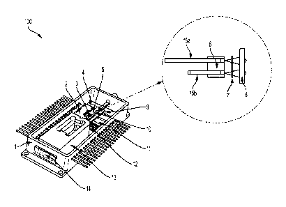
Chip package 100 includes a scanning unit 13, according to an embodiment.
Scanning unit 13
implements the B-scan allowing for 2D OCT scanning together with the A-scan
generated by
PIC 10, according to an embodiment. Scanning unit 13 provides the desired
scanning range
(e.g., 12 mm) at the focal plane. Additionally, the lateral resolution is
adjusted by scanning
unit 13 along the scanning range, thus guaranteeing the desired depth of
field. Scanning unit
13 may include a barrel (beam collimation) and a backbone (lateral scanning
and beam
focusing). Moreover, the total optical path of scanning unit 13 can be
adjusted since the barrel
can be moved back and forth along the backbone. This may be done to compensate
the
fabrication tolerances in the delay and dispersion compensating systems. FIG.
9 shows a 3D
mechanical model of scanning unit 13, according to an embodiment. A detailed
explanation
.. of an example scanning unit may be found in co-pending U.S. Application No.
14/118,629.
Chip package 100 includes an optical window 14 within a side of housing 1,
according to an
embodiment. Optical window 14 includes a material chosen to be substantially
transparent to
IR wavelengths (e.g., borosilicate glass). Optical window 14 is also assembled
with housing 1
to ensure a desired package hermeticity. FIG. 2 shows an example package
design that
includes a 14.4 mm x 5.1 mm N-BK7 glass window. The dimensions are chosen to
be
compatible with the scanning field of view from scanning unit 13, according to
an
embodiment.
PIC 10 and scanning unit 13 are aligned within housing 1 of chip package 100,
such that a
.. beam of light is coupled between the photonic integrated circuit and the
scanning unit. This
coupling efficiency is maximized based on the alignment, according to an
embodiment.
Scanning unit 13 is also positioned such that it scans the beam of light
across a focal plane
outside of chip package 100. The scanned beam of light crosses through optical
window 14.
Although not shown in FIG. 1, an optical source generates a beam of light that
is delivered to
chip package 100 via optical fiber 15a, according to an embodiment. The beam
of light is
output from fiber 15a and traverses both polarizer 7 and lens array 8 before
being coupled into
a waveguide on PIC 10, according to an embodiment. Fiber mount 6 is used to
help align
both fibers 15a and 15b with respective waveguides on PIC 10. As such, the
arrangement
including fiber mount 6, polarizer 7, and lens array 8 is provided to maximize
coupling
CA 2975945 2017-12-20
CA 02975945 2017-08-04
WO 2016/124762 PCT/EP2016/052549
-8-
efficiency of the light between the waveguides on PIC 10, and the optical
fibers. In another
example, the optical source is integrated within chip package 100.
This invention helps solve many miniaturized packaging problems in order to
make the PIC
resistant against moisture, shocks and thermally and mechanically harsh
environments.
Scanning unit 13 enabling B-scanning, and read-out electronics are also
assembled within the
10 same package, thus resulting in a fully-packaged 2D OCT system. Below,
various design
aspects of chip package 100 are described in further detail.
Light Coupling
A large coupling efficiency is desired between the light source and the PIC
10. The facets in
the ports of the PIC 10 are implemented by rib-type waveguides, according to
an
embodiment. The total height of the waveguide is around 3 um, with a slab
height of around
1.8 um, according to an embodiment. This fact translates into astigmatic
propagation modes,
thus resulting in different numerical apertures for the X and Y directions at
the PIC 10 end-
face (see FIG. 10). The beam profile of light propagating through an optical
fiber is shown in
FIG. 11. The coupling efficiency may be greatly increased by using
substantially rounded
modes with about the same numerical aperture for both axes in the waveguides
on PIC 10.
The coupling efficiency is estimated by the overlap integral, which is defined
as:
00
two E ribe, (x,y) E chip(x,y) dx
r = _____________________________________________________________________ (1)
f woo roc, lEfibõ12 dx dy roo f 7,0 lEchip 12 dx dy
Where Efiber and Echip are the electrical field propagating through the
optical fiber and the PIC
input waveguide respectively. In this particular example, the coupling
efficiency F = 27.25%
which translates into a coupling loss of 5.65 dB. This coupling loss is not
acceptable to reach
a large dynamic range in the OCT system. Thus, a mode matching between the
beam exiting
the optical fiber and the input waveguide is used to reduce the coupling loss,
according to an
embodiment.
FIG. 12 shows the coupling loss as a function of the mode field diameter (MFD)
of the light
beam launched into the PIC waveguide. Maximum coupling efficiency is reached
when the
input MFD is about 2.5 [tm as derived from Fig. 12. The fact of using optics
in-between the
optical fibers and PIC waveguides implemented on a different substrate
provides an extra
-9-
degree of freedom for the alignment process. This extra degree of freedom can
be used to
optimize the coupling efficiency, since the relative position between the
optical fibers and
lens array 8 can be controlled. Figure 13 shows how to benefit from the
magnification given
by the lens 8 in order to relax the alignment tolerances. For simplicity, Fig.
13 only illustrates
one of the four channels. In particular, a tolerance accuracy of 5h at the
waveguide input 1302
(MFD = SD = 2.5 pm) is translated into a tolerance accuracy of m times 5h at
the fiber input 1304
(MFD = 9.2 pm), where m is the lens magnification. In this case, the
magnification may be
set to 9.2/2.5 = 3.68.
Figure 14 shows example ray-trace simulations between an optical fiber 1402
and a waveguide 1404 and
the design lengths of the fiber-to-chip focusing system. A coupling efficiency
of up to 86% has been
theoretically and experimentally demonstrated by using this solution.
Consequently, this solution can
meet a coupling requirement of < ldB.
Other solutions such as butt coupling or lensed/tapered fiber v-groove array
do not benefit
from the above-mentioned advantage. On one hand, the alignment tolerances will
be imposed
by the accuracy of the align & attach process for butt coupling. Moreover,
prohibited coupling
loss larger than 5 dB is reached by this technique. On the other hand, apart
from the accuracy
of the align & attach process, the mechanical tolerances of the v-groove chip
and fibers
positioning could have a strong impact.
Figure 15 shows this effect. The typical tolerance of the fibers being
assembled on an
example v-groove chip 1502 is 1 pm. Figure 15 illustrates a first fiber
actual core position 1504, a last
fiber actual position 1506, an ideal fiber core center line 1508, an actual
fiber core position 1510, and an
an ideal fiber core position 1512. Figure 16 shows the coupling loss for a MFD
of 2.5 um when it is
misaligned with respect to the waveguide. As depicted in Fig. 16, this
tolerance is not acceptable to fulfill a
coupling loss target of < ldB.
The alignment between the PIC output waveguides (balanced detection) and the
PIC is a key
factor limiting the SNR performance of the OCT system. The separation distance
between the
waveguide end facets and photo-diode army 3 (hereafter referred as is')
depends on the
numerical aperture of the waveguides, which is 0.39 for both the x and y
coordinates,
according to one example, and the accuracy of the alignment process. The spot
diameter in the
waveguide is calculated to be 2.3 um for both the x and y coordinates
respectively, in this
example. On the other hand, the active area diameter of the photodiodes is 70
pm, according
to one example.
CA 2975945 2018-07-04
- 10 -
FIGs. 17A and 17B show 3D plots of the coupling efficiency for two different
cases in which
s = 10 pm and s = 50 pm, respectively. As expected, the maximum tolerances
become lower
as the distance s increases,
The permissible tolerances in order to achieve a coupling efficiency greater
than 95% (0.22
dB coupling loss) as a function of the distance s (from 0 to 70 lam with 5 pin
step) can be seen
in Fig. 18, according to one example. Attending to the spatial tolerance
values in the order of
several m, the alignment between the PIC 10 and photodiode array 3 can be
passive, i.e., no
need of monitoring the photo-current detected by photodiode array 3 during the
alignment,
even considering a separation distance s = 70 pm.
Thermal Management
A custom thermal design is required to dissipate the large heat load generated
by PIC 10.
Otherwise, the base temperature of PIC 10 will increase and effects such as
the stress
mediated by the material thermal expansions will result in misalignment
between parts.
Moreover, thermal effects in silicon such as the two-photon absorption will
impact on the
optical performance of F'IC 10, degrading the final SNR.
The temperature on the top side of heat spreader 4 should be kept fixed to
avoid lack of
optical performance depending on the temperature due to undesired
misalignments. An
example stack of materials considered for the thermal design of a heat sink is
shown in FIG.
19. The heat sink includes both heat spreader 4 and cooling element 9,
according to an
embodiment, The total amount of heat transferred from the heat source through
the heat sink
should be maximized. The thermal resistances of PIC 10, heat spreader 4,
cooling element 9, and the
base 1902 of chip package 100 may be fixed by manufacturing materials and
thickness. FIG. 19 illustrates
PLC 10, a thermal adhesive 1904, heat spreader 4, a thermal adhesive/solder
preform 1906, cooling
element 9, another thermal adhesive/solder preform 1908, and a package base
1902. In one example,
PIC 10 has a thickness around 0.67 mm, heat spreader 4 has a thickness around
1.75 mm, and cooling
element 9 has a thickness around 1.6 mm. The heat load (Q) to be dissipated is
about 20W, according to
one example. If the heat sink can manage the dissipation of a temperature
gradient (AT) with respect to
the room temperature, then the total thennal resistance (Rt) must be lower
than:
R. Lic < AT [k1
(2)
e Q [W]
CA 2975945 2018-07-04
CA 02975945 2017-08-04
WO 2016/124762 PCT/EP2016/052549
-11-
Where Rt is the sum of all the thermal resistances corresponding to the stack
of materials
given in Equation (3):
Rt [71 = Rp RAi Rgs + RA2 + RTEc + RA3 + Rpg Rgaõ (3)
Where Rptc, RHS, RIEC, and Rbase are thermal resistances of the PIC, heat
spreader, cooling
element, and chip package base, respectively. Also, RAt, RA?, and RA3 are
thermal resistances
of the adhesive layers. Thus, the thermal resistance may be defined as:
Rt 1--k 1 = t [m]
IWi A [1n2i.a[rSci (4)
With t being the thicknessõ4 the cross-sectional area and a the thermal
conductivity,
respectively. Consequently, the thickness and the material for the parameters
RAi, RA2 and
RA3 should be properly designed. The bond-line thickness is at the end limited
by the
planarity of parts positioned up and down and the thermal conductivity and
depends on the
material. Generally, solder preforms featuring the same thickness than an
adhesive result in
lower thermal resistances. The main factor limiting the thermal performance of
an adhesive is
the proportion of voids in a certain volume.
Hermeticity
Moisture penetrating the package results in corrosion and internal
condensation (depending on
ambient conditions). Generally, the presence of moisture at an interface
between dissimilar
metals accelerates corrosion. Additionally, epoxy joints being affected as
moisture is absorbed
translates into potentially weakening the joints; therefore causing
performance drops as the
epoxy expands. Moisture penetrating the package results in corrosion and
internal
condensation (depending on ambient conditions). Therefore, an hermetic
solution would be
highly desired.
Fully hermetic solutions involve very complex part design and assembly steps,
driving up the
total cost. Consequently, quasi-hermetic approaches are usually assembled in
the industry.
The larger the degree of hermeticity, the larger the cost will become.
CA 02975945 2017-08-04
WO 2016/124762 PCT/EP2016/052549
- 12-
Hermeticity in electro-optical packaging is defined as the leakage rate
measured in cm3 per
second at a certain atmospheric pressure. A large degree of hermeticity is
determined by the
package design and manufacturing. As an exemplary case, Fig. 2 shows the
hermeticity value
reached by the package (< 1-10-8 atm. cm3/s). However, this value will depend
on the quality
of the lid sealing and the solder performance of the optical window to the
package and the
metal ferrule of the fiber mount element to the pipe, according to an
embodiment. A typical
degree of hermeticity used by the laser industry, which involves the packaging
of electro-
optical components is < 1.10-8 atm. cm3/s.
Delay and Dispersion Balance
Sample and reference arms in an OCT system interferometer must be balanced in
terms of
accumulated delay and dispersion. As the optical subassembly may be subject to
different
designs, it may be important to implement an adjustable delay and dispersion
compensation
system in the reference arm. hi this way, the PIC design would be transparent
to the scanning
unit design.
Both sample and reference arms are balanced on-chip in the particular design
of Fig. 1. As a
consequence, the effect of the scanning unit 13 is required to be compensated
somewhat in the
reference arm. For this purpose, an optical fiber with a mirrored end (fiber
15b in FIG. 1) has
been implemented in the reference arm as illustrated in Fig. 8. Figure 20
shows this concept.
The accumulated phase as a function of the wavelength for both the sample and
reference
arms should be equal, as depicted in Equation (5) below.
27/ N 27r m
It's (A) = (Pr (2) Ei-i n (A) = L = E --1 n - (2) = L (5)
Ao Ao
Delay imbalance beyond the coherence length along the axial scanning range
does not allow
for OCT interference generation, and thus, the system becomes generally
unusable. Fine
adjustment may be performed by means of thermo-optical actuators within the
PIC, at the
expense of higher power consumption.
On the other hand, the importance of compensating dispersion relies on the
loss of OCT axial
resolution. Actually, according to Eq. 6, the higher the dispersion imbalance,
the wider the
full-width-half-maximum (FWHM) of the axial point spread function (PSF)
becomes.
- 13-
2 112
aT [ac2 t(DsiLsi D1system)AAC11
(6)
where c is the speed of light in vacuum, ,a1 the source bandwidth, Dsi the
group velocity
dispersion (GVD) in silicon, Ls, half of the length difference between the
arms in silicon,
Dlsystem all the extra dispersive components in the system (dispersion*length)
that contribute
to the PSF broadening and finally, ac stands for the coherence length defined
by:
21n2 A02
(7)
Read-out Output Signals
Very low-amplitude signals are detected at the output of a typical OCT system.
If these
signals would be directly connected to the package pins, then the signals
would be too weak
to be useable.
According to an embodiment, photodiode array 3 translates light combined from
sample and
reference paths into electrical interference patters with peak amplitudes in
the microamp
range and frequencies above Megahertz range. These weak differential signals
should be
amplified before exiting the package so as to avoid SNR degradation. An
impedance
adaptation network followed by a differential low-noise Trans Impedance
Amplifier (T1A) 2102
can raise the weak signals up to the millivolt range (TIA gain above 80K) and
also keep the
noise floor low which maximizes the SNR. The electronics are included on a
circuit board
that is glued onto the heat spreader, very close to the photodiode array in
order to shorten the
length of wires, as illustrated in FIG. 21. The design also includes well
adapted monitor
outputs for alignment and verification procedures.
Lateral Scanning and Focusing
According to an embodiment, the PIC 10 implements depth-scans (A-scan) while
the scanning
unit 13 implements lateral scanning capability (B-scan). Scanning unit 13
provides a desired
scanning range at a designed focal plane outside of the chip package.
Moreover, the lateral
resolution fulfilling the required depth of field should also be implemented
by scanning unit
13. An example assembly of scanning unit 13 is depicted in FIG. 22. The
housing is built by
CA 2975945 2018-07-04
11
-14-
two stainless steel pieces, the barrel 2202 and the backbone 2204, according
to an embodiment. The barrel
2202 accounts for the beam collimator which includes an aspherical lens 2206
inside. The backbone
backbone 2204 accounts for the lateral scanner, performed by a 60 degrees
angled prism 2208 and one
magnetic MEMS 2210; and also the focusing optics by means of a doublet element
2212, according to
an embodiment. The beam of light that exits from the PIC 10 is collimated at
scanning unit 13 with the
.. aspheric lens 2206, and then is sent to the prism 2208 that is located
below the MEMs mirror 2210. The
beam of light is then sent to the focusing doublet lens 2212 and finally exits
the chip package through
optical window 14.
As already mentioned, optical delay and dispersion should be balanced in OCT
systems. A
fiber with a mirror end is used in reference to compensate delay and
dispersion induced by
scanning unit 13. However, fiber cut tolerances are about lmm which is almost
half of the
axial scanning range. In order to compensate such tolerance, the barrel of the
scanning unit
may be extracted/inserted into the backbone and thus, increase or decrease the
sample optical
path without affecting the scanning range or resolution, according to an
embodiment.
An assembly tolerance analysis (from 36-90 degrees of operation temperature)
may be
performed according to the tolerances provided by the manufacturers of the
optical
components. The criterion that is set for the tolerance analysis is the RMS
spot radius.
According to one example, the results indicate that: (1) in order not to
exceed the 1mm from
the nominal focus position, the tolerance on the distance between the source
and the asphere
is about 0.02mm; (2) the tolerance on decentre of the asphere is 0.05mm and
on the tilt
tolerance is 0.1 degrees; (3) the tolerance on the tilt of the MEMs mirror in
the non-scanning
direction is 0.7 degrees. For larger values the beam is being clipped on the
doublet; and (4)
the tolerance on decentre of the entire backbone with respect to the source on
both axes is
0.05mm and on the tilts is 0.5 degrees. Therefore, active alignment between
PIC 10 and the
scanning unit 13 may be required.
Polarization
Light traveling through the one or more waveguides on the PIC 10 suffers from
polarization
rotation along both, the sample and reference paths of the interferometer.
Even if a linear TE
polarization, with high PER (polarization extinction ratio) is launched into
the PIC 10,
structures like bends or curves will transfer part of the energy into the
orthogonal polarization
(TM). The birefringence in silicon induces significant delay difference
between both
CA 2975945 2018-07-04
CA 02975945 2017-08-04
WO 2016/124762 PCT/EP2016/052549
- 15 -
polarizations. Such delay difference translates into undesired double OCT
images after these
polarizations beats in the detector.
Suppressing the undesired polarization prior to detection is one solution to
avoid double OCT
images. A polarizing element 7 is employed for the orthogonal and undesired
polarization
suppression, according to an embodiment. On one side, polarizing element 7
assures that only
the light aligned along the main polarization axis will enter the PIC 10. This
way, high PER is
guaranteed and thus, polarization beatings across the PIC 10 are minimized. On
the other side,
light coupled in/out of the reference fiber (e.g., 15b) is filtered in the
same way. Polarization
rotation from the reference fiber coupling into the PIC and into the detector
is depreciable.
Therefore, the reference path provides a linear and clean polarization. Even
if the sample path
transfers energy into the undesired polarization by rotation, only the desired
polarization will
be beaten with reference in the photodetector and thus, no double images will
be generated.
Wire Bonding
The axial scanning (A-scan) may be carried out by means of thermo-optical
effects in silicon,
according to an embodiment. High density molybdenum heaters deposited along
the
waveguides may provide heat transfer to perform the full axial scan. Au/A1
contact pads may
be used to connect these heaters to the package pins.
The large number of contact pads, among others, complicates the wire-bonding
process
directly from the PIC 10 to the pins of the chip package. One solution aims at
using interposer
11 as illustrated in Fig. 23. Such an element provides a connection map
between the PIC 10
and package pins. It can combine and, therefore, simplify wire connections
coming from
various elements used in particular structures. Interposer 11 decreases the
wires length and
also, facilitates the use of multiple wires so as to reduce the current
density.
Chip Package Assembly
The various components within chip package 100 are assembled and aligned to
maximize the
use of space within housing 1 and to maximize coupling efficiency of a beam of
light passing
between the various optical components, according to an embodiment. PIC 10 may
first be
bonded to heat spreader 4, which acts as an upper layer of a heat sink. The
heat sink may also
include a cooling element bonded to the interior of housing 1. Solder may be
used for
attaching the heat sink to the housing interior of chip package 100.
CA 02975945 2017-08-04
WO 2016/124762 PCT/EP2016/052549
- 16 -
Photodiode array 3 should be aligned with an optical output from PIC 10 and
placed into the
chip package, according to an embodiment. Careful alignment of photodiode
array 3 may be
carried out using a process depicted generally in FIGs. 24 ¨ 28, according to
an embodiment.
FIG. 24 illustrates an alignment tool 2400 that includes a 6-axis platform
2402, a gripper body
2404, and pneumatic lines 2406a and 2406b used to open and close the jaws of
gripper body
2404. Gripper body 2404 is designed to hold a specific part 2408 to be
aligned. In this case,
part 2408 is the photodiode array 3 as shown more clearly in the close up view
of gripper
body 2404 illustrated in FIG. 25. FIG. 25 also shows with the double-ended
arrows the
movement of the pincers that hold and release part 2408.
FIG. 26 illustrates a clamp structure 2600 that includes a set of pogo-style
pins 2602. The
bottom part of pins 2602 make contact with part 2408 while the top part of
pins 2602 can
attach to electrical flying leads to be connected to external testing
equipment, according to an
embodiment. Pins 2602 may have a pitch around 0.5 mm.
FIG. 27 illustrates the connection made between pins 2602 and part 2408. In
this example,
part 2408 is a photodiode array to be placed within chip package 100. FIG. 28
displays
another view where clamp structure 2600 is seen resting over gripper body
2404.
Once the photodiode array has been carefully aligned and placed within chip
package 100,
lens array 8 is aligned to PIC 10 as well, and placed within chip package 100.
In order to
facilitate the handling of lens array 8, lens array 8 may first be attached to
a post, according to
an embodiment. The post is then mechanically manipulated to align the lens
array with the
waveguides on PIC 10.
The alignment procedure of lens array 8 does not involve active coupling to
optical fibers
which would be extremely complex. Instead an optical beam profiler is used to
launch optical
power into the PIC in the reverse direction compared to how light is guided in
the fully
completed module, according to an embodiment. In this way, optical power is
made to emit
from the PIC inputs, which then transmits through the lens array in the
reverse direction
during active alignment. The optical power that is transmitted from the lens
array is detected
on a distant beam profiler. This set up is illustrated in FIGs. 29 and 30,
with the lens elements
actually be used in the alignment circled in FIG. 29. Furthermore, FIG. 31
shows this reverse
optical routing concept through the PIC. The shape of the beam footprints that
are incident on
- 17 -
the profiler can be used to infer collimation and off-axis misalignments. This
information
allows lens array 8 to be optimally aligned, followed with adhesive attach to
the heat sink.
Next, the fiber mount 6 may be aligned and attached, such that optical fibers
mounted in the
fiber mount 6 are aligned to the lens array 8. The placement of fiber mount 6
may be important
for the overall operation since it aligns the optical fibers (15a and 15b) to
the waveguides on
PIC 10. FIG. 32 illustrates the positions and optical routing corresponding to
a well aligned
optical assembly of a fiber mount (TVA' in the figure) to a PLC 10. Initially,
the FVA source
fibre (15a in the figure) is aligned to the PIC Compensator waveguide 3202. A
photocurrent
signal may be used to determine when the FVA is optimally aligned. Next, the
FVA is
manually translated horizontally that the source fibre 15a is aligned
approximately with a different
.. PIC waveguide.
A lens assembly may then be used and, by manipulating the position of the lens
relative to the
PIC output, a pseudo-collimated beam can be generated. By translating the lens
position
left/right in the package, the beam can be made to steer approximately along
the axis of the
package and emerge centrally from the package window aperture. A multimode
fibre
.. assembly is placed in line with this beam, outside the package, in order to
collect some of this
light. In this way, optimal rotation angles can be found as illustrated
schematically in FIG. 33.
Afterwards, scanning unit 13 may be aligned and attached using a similar
alignment
arrangement as depicted in FIGs. 24 ¨ 28. The alignment between scanning unit
13, PIC 10,
photodiode array 3, and optical fibers 15a and 15b is performed so as to
maximize a coupling
efficiency of a beam of light traveling between each of the components,
according to an
embodiment.
Wire bonding may be performed to attach the various electrical leads to pins
of the chip
package. Finally, any seams around the outside of chip package 100 may be
sealed to improve
hermeticity.
FIG. 34 illustrates an example assembly method 8400 for placing various
components within
a chip package, according to an embodiment.
Method 3400 begins at block 8402 where a photonic integrated circuit (PIC) is
attached to a
heat sink. The FTC may be attached to a heat spreader layer of the heat sink.
The heat sink
may already be attached to a base of the chip package. Typically, one side of
the PIC
CA 2975945 2018-07-04
CA 02975945 2017-08-04
WO 2016/124762 PCT/EP2016/052549
- 18 -
includes an active layer including waveguides and opto-electrical components
while the
opposite side is bonded to the heat sink.
At block 8404, a photodiode array is also attached to the heat sink, according
to an
embodiment. The photodiode array may be attached to the heat spreader layer of
the heat
sink. The photodiode array may collectively be called a photodetector. Many
types of
photodetectors may be used including CMOS based, CCD, reverse-biased LEDs,
etc.
At block 8406, a fiber mount is attached to the heat sink, according to an
embodiment. The
fiber mount may be attached to the heat spreader layer of the heat sink. The
fiber mount is
attached such that optical fibers are aligned to waveguide inputs on the PIC.
A lens array and
polarizing element may also be used between the fiber mount and PIC. The lens
array should
also be aligned between the fiber mount and PIC waveguide to ensure that light
is focused
correctly onto the waveguide facet on the PIC.
At block 8408, a scanning unit is attached to the package base, according to
an embodiment.
Each of the PIC, photodiode array, scanning unit, and fiber mount are aligned
within the
package such that light may be coupled between the elements, and more
specifically, so that
the coupling efficiency is maximized as light passes between the elements,
according to an
embodiment.
Closing Remarks
It is to be appreciated that the Detailed Description section, and not the
Summary and
Abstract sections, is intended to be used to interpret the claims. The Summary
and Abstract
sections may set forth one or more but not all exemplary embodiments of the
present
invention as contemplated by the inventor(s), and thus, are not intended to
limit the present
invention and the appended claims in any way.
Embodiments of the present invention have been described above with the aid of
functional
building blocks illustrating the implementation of specified functions and
relationships
thereof. The boundaries of these functional building blocks have been
arbitrarily defined
herein for the convenience of the description. Alternate boundaries can be
defined so long as
the specified functions and relationships thereof are appropriately performed.
The foregoing description of the specific embodiments will so fully reveal the
general nature
of the invention that others can, by applying knowledge within the skill of
the art, readily
modify and/or adapt for various applications such specific embodiments,
without undue
CA 02975945 2017-08-04
WO 2016/124762 PCT/EP2016/052549
- 19 -
experimentation, without departing from the general concept of the present
invention.
Therefore, such adaptations and modifications are intended to be within the
meaning and
range of equivalents of the disclosed embodiments, based on the teaching and
guidance
presented herein. It is to be understood that the phraseology or terminology
herein is for the
purpose of description and not of limitation, such that the terminology or
phraseology of the
present specification is to be interpreted by the skilled artisan in light of
the teachings and
guidance.
The breadth and scope of the present invention should not be limited by any of
the above-
described exemplary embodiments, but should be defined only in accordance with
the
following claims and their equivalents.