Note: Descriptions are shown in the official language in which they were submitted.
Magnetic Flux Control in Superconducting Devices
TECHNICAL FIELD
The present disclosure relates to magnetic flux control in superconducting
devices.
BACKGROUND
Quantum computing is a relatively new computing method that takes advantage of
quantum effects, such as superposition of basis states and entanglement to
perform certain
computations more efficiently than a classical digital computer. In contrast
to a digital computer,
which stores and manipulates information in the form of bits (e.g., a "1" or
"0"), quantum
computing systems can manipulate information using qubits. A qubit can refer
to a quantum
device that enables the superposition of multiple states (e.g., data in both
the "0" and "1" state)
and/or to the superposition of data, itself, in the multiple states. In
accordance with conventional
terminology, the superposition of a "0" and "1" state in a quantum system may
be represented,
e.g., as a I 0> + f Ii>. The "0" and "1" states of a digital computer are
analogous to the I 0> and
1> basis states, respectively of a qubit. The value I a I 2 represents the
probability that a qubit
is in I 0> state, whereas the value 13 I 2 represents the probability that a
qubit is in the I 1>
basis state.
SUMMARY
According to an aspect, there is provided a device comprising: a first qubit
comprising a
first co-planar waveguide; a second qubit comprising a second co-planar
waveguide, wherein the
second co-planar waveguide crosses the first co-planar waveguide; and a qubit
coupler
comprising a loop having a first lobe and a second lobe, wherein a first
portion of the first lobe
extends parallel to the first co-planar waveguide, a second portion of the
first lobe extends
parallel to the second co-planar waveguide, a first portion of the second lobe
extends parallel to
the first co-planar waveguide, and a second portion of the second lobe extends
parallel to the
second co-planar waveguide.
Implementations of the devices may include one or more of the following
features. For
example, in some implementations, the devices include multiple ground pads
arranged around a
1
CA 2977780 2019-12-11
position where the second co-planar waveguide crosses the first co-planar
waveguide. The
multiple ground pads may consist of four ground pads arranged in a two-by-two
array. Each
ground pad of the multiple ground pads may be connected to multiple
superconducting
airbridges. For each ground pad of the multiple ground pads, at least one
superconducting
airbridge of the multiple superconducting airbridges may connect the ground
pad to a ground
plane. For each ground pad of the multiple ground pads, the at least one
superconducting
airbridge that connects the ground pad to the ground plane may be located at
approximately a
center of a corresponding side of the ground pad. For each ground pad of the
multiple ground
pads, at least one superconducting airbridge of multiple superconducting
airbridges may connect
the ground pad to an adjacent ground pad. A first ground pad of the multiple
ground pads may be
located within a first lobe of the qubit coupler, and a second ground pad of
the multiple ground
pads may be located within a second lobe of the qubit. The first lobe and the
second lobe may be
arranged diagonally with respect to one another around the position where the
second co-planar
waveguide crosses over the first co-planar waveguide.
In some implementations, the qubit coupler includes a tilt bias line connected
to the
second lobe, and the devices further include at least one superconducting
airbridge crossing over
the tilt bias line, in which a first end of each superconducting airbridge is
connected to a ground
plane on a first side of the tilt bias line, and a second end of each
superconducting airbridge is
connected to a ground plane on a second side of the tilt bias line that is
opposite to the first side.
Each superconducting airbridge crossing over the tilt bias line may be
elongated in a direction
that is orthogonal to a direction of current flow through a portion of the
tilt bias line over which
the superconducting airbridge crosses.
In some implementations, the qubit coupler includes a superconducting quantum
interference device (SQUID) bias line connected to the first lobe through an
elongated
superconducting trace, and the devices further include at least one
superconducting airbridge
crossing over the elongated superconducting trace, wherein a first end of each
superconducting
airbridge is connected to a ground plane on a first side of the elongated
superconducting trace,
and a second end of each superconducting airbridge is connected to a ground
plane on a second
side of the elongated superconducting trace that is opposite to the first
side. Each
superconducting airbridge crossing over the elongated superconducting trace
may be elongated
2
CA 2977780 2019-12-11
in a direction that is orthogonal to a direction of current flow through a
portion of the elongated
superconducting trace over which the superconducting airbridge crosses.
In some implementations, each of the first lobe and the second lobe encircles
a
corresponding ground plane gap-region. The devices may further include two
additional ground
plane gap-regions from which the ground plane has been entirely removed, in
which each ground
plane gap-region is approximately the same area, and in which the ground plane
gap-regions are
arranged in quadrants around a position where the second co-planar waveguide
crosses over the
first co-planar waveguide.
In some implementations, the devices include: a first substrate, in which the
first qubit,
the second qubit, and the qubit coupler are arranged on the first substrate; a
second substrate
bonded to the first substrate; and multiple bump bonds between the first
substrate. The qubit
coupler may include a tilt bias line connected to the second lobe and a first
elongated
superconducting trace connected to the first lobe. The devices further may
include: a ground
plane on the first substrate, in which a first portion of the ground plane is
adjacent to a first side
of the tilt bias line and a second portion of the ground plane is adjacent to
a second side of the tilt
bias line that is opposite to the first side; and a second superconducting
trace on the second
substrate, in which a first bump bond connects the first portion of the ground
plane to a first end
of the superconducting trace, and a second bump bond connects the second
portion of the ground
plane to a second end of the second superconducting trace. The second
superconducting trace
may cross over a portion of the tilt bias line on the first substrate, and may
be elongated in a
direction that is orthogonal to a direction of current flow through the
portion of the tilt bias line
over which the second superconducting trace crosses. The devices further may
include: a ground
plane on the first substrate, in which a first portion of the ground plane is
adjacent to a first side
of the elongated first superconducting trace and a second portion of the
ground plane is adjacent
to a second side of the elongated first superconducting trace that is opposite
to the first side; and
a second superconducting trace on the second substrate, in which a first bump
bond connects the
first portion of the ground plane to a first end of the second superconducting
trace, and a second
bump bond connects the second portion of the ground plane to a second end of
the second
superconducting trace. The second superconducting trace may cross over a
portion of the
elongated first superconducting trace on the first substrate, and may be
elongated in a direction
3
CA 2977780 2019-12-11
that is orthogonal to a direction of current flow through the portion of the
elongated first
superconducting trace over which the second superconducting trace crosses.
In some implementations, the qubit coupler includes an approximately
lemniscate shape.
In some implementations, the first lobe and the second lobe are arranged
diagonally with
respect to one another around a position where the second co-planar waveguide
crosses over the
first co-planar waveguide.
In some implementations, the qubit coupler crosses over the first co-planar
waveguide
and over the second co-planar waveguide.
In some implementations, an airgap is between the second co-planar waveguide
and the
first co-planar waveguide at a position where the second co-planar waveguide
crosses over the
first co-planar waveguide.
In some implementations, each of the first qubit and the second qubit is a co-
planar
waveguide flux qubit.
According to another aspect, there is provided a device comprising: a first
qubit; a second
qubit; and a qubit coupler comprising a loop comprising a first lobe and a
second lobe, wherein
each of the first lobe of the loop and the second lobe of the loop is arranged
to allow coupling
between the first qubit and the second qubit, and wherein the loop comprises a
co-planar
waveguide that crosses over itself.
Particular implementations of the subject matter described here can realize
one or more
of the following advantages. For example, in some implementations, the tunable
qubit coupler
having the substantially lemniscate shape may increase the mutual inductance
of associated with
the first qubit and qubit coupler element (e.g., M(qubitl-coupler)), as well
as the mutual
inductance associated with the second qubit and qubit coupler element (e.g.,
M(coupler-qubit2).
Additionally, the tunable qubit coupler of the present disclosure may increase
the overall qubit-
qubit coupling, by increasing mediated qubit to qubit coupling inductance
(e.g., M(qubitl-
coupler-qubit2)) relative to direct qubit to qubit coupling inductance (e.g.,
M(qubitl-qubit2)). By
using a single loop that crosses over itself to establish an approximately
lemniscate or
gradiometer shape, a number of control elements for the coupler element may be
reduced.
Additionally, in some implementations, the approximately lemniscate or
gradiometer shape of
the coupler may help reduce coupler size requirements allowing for an increase
in the number of
4
CA 2977780 2019-12-11
circuit elements (e.g., increase in number of qubits) formed on a substrate.
By introducing
ground plane gap regions, it is possible, in some implementations, to provide
a zero net mutual
or direct inductance between two qubits. Furthe'more, by providing airbridge
crossover
structures, lower impedance pathways for return current relative to pathways
along the edges of
ground planes may be provided, leading in some implementations to a reduction
in crosstalk.
The details of one or more implementations are set forth in the accompanying
drawings
and the description below. Other features and advantages will be apparent from
the description,
the drawings, and the claims.
BRIEF DESCRIPTION OF THE DRAWINGS
FIG. 1A is a schematic illustrating a top view of an example of a qubit
coupling
architecture for a quantum computing processor.
FIG. 1B is a schematic illustrating a close-up view of the qubit coupling
architecture of
FIG. 1A.
FIG. 2 is a circuit schematic that illustrates the equivalent circuit diagram
of the qubit
coupling architecture of FIG. 1A.
FIG. 3 is a schematic illustrating an example of the sign of mutual inductance
as a result
of qubit coupler current flow in different regions around a crossover point
between a first and
second qubit.
CA 2977780 2019-12-11
FIG. 4 is a schematic illustrating an example of the sign of mutual inductance
as a
result of qubit coupler current flow for a qubit coupler element having a
layout depicted
in FIG. 1B.
FIG. 5 is a schematic illustrating a top view of an example of a qubit
coupling
architecture for a quantum computing processor.
FIG. 6 is a schematic that illustrates a top view of an example of a qubit
coupling
architecture for a quantum computing processor.
FIG. 7A is a schematic that illustrates a close-up view of a region within the
structure depicted in FIG. 1B.
FIG. 7B is a schematic that illustrates a close-up view of a region within the
structure depicted in FIG. 1B.
FIG. 8 is a schematic that illustrates a side view of a quantum processor that
includes a first chip bonded to a second chip.
FIG. 9 is a photograph that shows an example of a first chip including qubit
coupling architecture for a quantum processor.
DETAILED DESCRIPTION
Quantum computing entails coherently processing quantum information stored in
the quantum bits (qubits) of a quantum computer. Superconducting quantum
computing
is a promising implementation of quantum computing technology in which quantum
computing circuit elements are formed, in part, from superconducting
materials.
Superconducting quantum computers are typically multilevel systems, in which
the two
lowest energy levels are used as the computational basis.
In certain types of quantum computing processors, such as quantum annealers,
the
qubits of the quantum processor are coupled together in a controllable manner
such that
the quantum state of each qubit affects the corresponding quantum states of
the other
qubits to which it is coupled. Depending on the processor design, the chosen
architecture
may limit the density and total number of qubits available for coupling, and
thus limit the
ability of the processor to perform complex problems requiring large numbers
of qubits.
6
CA 2977780 2017-08-30
Furthermore, in certain quantum computing designs, the qubits may suffer
energy loss
and decoherence due to interactions with two level systems. Accordingly, to
improve the
perfounance of a quantum computing system, such as a quantum annealer, it is
useful to
provide an architecture that achieves high connectivity across qubits, with a
compact
coupler footprint, strong qubit to qubit coupling, and low levels of
crosstalk.
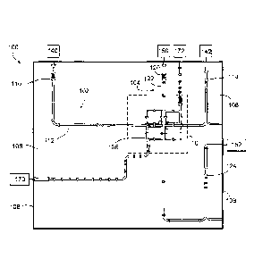
FIG. lA is a schematic that illustrates a top view of an exemplary qubit
coupling
architecture 100 for a quantum processor. A quantum processor may be a
physical system
that includes one or more quantum infomiation processing devices, e.g., one or
more
qubits, and that is used to perfolin quantum computations or simulations. The
type of
physical system included in the quantum processor may depend on the type of
quantum
processor and the computations to be performed. For example, in some cases,
the
quantum processor may be a quantum annealing device that includes a circuit of
superconducting qubits, e.g., phase qubits, flux qubits, such as co-planar
waveguide flux
qubits, transmon qubits, gmon qubits, or other types of qubits. The qubit
coupling
architecture 100 shown in the example of FIG. lA may be used as a quantum
annealer.
Alternatively, the qubit coupling architecture may be used for other types of
quantum
processors, such a quantum simulator.
FIG. 1B is a schematic illustrating a close-up view of the qubit coupling
architecture 100 of FIG. lA contained within the region 10. The quantum
annealer
includes a first qubit 102, a second qubit 104, and a qubit coupler element
106 for
coupling the first qubit 102 to the second qubit 104. The quantum annealer
also includes
a ground plane 108 formed from a superconducting material and arranged at
various
locations around the qubits and the qubit coupler. The qubits 102, 104, the
qubit coupler
element 106 and the ground plane 108 are formed on a dielectric substrate,
such as silicon
or sapphire. Though the architecture shown in FIG. lA includes only two qubits
and a
single qubit coupler element, the architecture can be expanded to include
additional
qubits (e.g., 4, 6, 8, 10, 20, 30, 40, 50, 100, 1000 or more) and additional
qubit couplers
(e.g., 2, 3,4, 5, 10, 15, 20, 25, 50, 100, 500 or more).
7
CA 2977780 2017-08-30
Each of the first qubit 102 and the second qubit 104 shown in the example of
FIG.
lA is a co-planar waveguide flux qubit (also referred to as a "fluxmon
qubit"). A
fluxmon qubit includes a superconducting co-planar waveguide that is coupled
in parallel
with a superconducting quantum interference device (SQUID). For example, the
first
qubit 102 includes a first SQUID 110 coupled to a first end of a first co-
planar waveguide
112. A second end 114 of the first co-planar waveguide 112 is tied to the
ground plane
108. Similarly, the second qubit 104 includes a second SQUID 120 coupled to a
first end
of a second co-planar waveguide 122. A second end 124 of the second co-planar
waveguide 122 is tied to the ground plane 108. The first and second co-planar
waveguides 112, 122 are arranged on the substrate as elongated thin film
traces of
superconducting material, each of which is separated from the ground plane 108
by co-
extensive gaps on either side of the elongated trace. The superconducting
materials used
to form the co-planar waveguides 112, 122, the SQUIDs 110, 120, and the ground
plane
108 include materials exhibiting superconducting properties at or below a
superconducting critical temperature, such as aluminum (superconducting
critical
temperature of 1.2 kelvin) or niobium (superconducting critical temperature of
9.3
kelvin).
Each of the qubits 102, 104 is couplable to tunable qubit control elements for
controlling the operation of the qubits. The tunable qubit control elements
may be located
on the same chip on which the qubits are formed or located on a separate chip.
The type
of tunable qubit control elements is dependent on the type of physical system
included in
the quantum processor. For example, in cases where the quantum processor
includes a
system of superconducting qubits, e.g., arranged as a superconducting circuit,
the tunable
qubit control elements may provide biases that are proportional to externally
applied
voltages or currents that effect changes in the superconducting qubits. Each
configuration
of the applied biases may have a different effect on the quantum processor.
The qubit control elements can include, e.g., a SQUID bias control element and
a
tilt bias control element. For example, the first qubit 102 may be coupled to
a first
SQUID bias control element 140 and coupled to a first tilt bias control
element 142.
8
CA 2977780 2017-08-30
Similarly, the second qubit 104 may be coupled to a second SQUID bias control
element
150 and coupled to a second tilt bias control element 152. A tilt bias control
element
provides control signals (e.g., flux biases) to tilt/perturb the double well
potential during
operation of the qubit, whereas a SQUID bias control element provides control
signals
(e.g., flux biases) to adjust a magnitude of the barrier between the potential
wells during
operation of the qubit or to change the operating frequency of the qubit.
Additional
control functions with the qubit control elements are also possible. Further
details on the
structure, fabrication and arrangement of flux qubits can be found, e.g., in
WO
2017/058194.
The qubit coupler element 106 includes an elongated superconducting trace and
a
SQUID 160 arranged in a loop, and is used to allow coupling between the first
qubit 102
and the second qubit 104. Similar to the co-planar waveguides of the qubits,
the
elongated trace of the qubit coupler element 106 is formed from a material
exhibiting
superconducting properties at or below a superconducting critical temperature,
such as
aluminum (superconducting critical temperature of 1.2 kelvin) or niobium
(superconducting critical temperature of 9.3 kelvin).
The qubit coupler element 106 also is couplable to tunable coupler control
elements for controlling the coupling between qubits. Similar to the tunable
qubit control
elements, the tunable coupler control elements may provide biases that are
proportional
to externally applied voltages or currents that effect changes in the
superconducting qubit
coupler element. Each configuration of the applied biases may have a different
effect on
the quantum processor. As an example, the SQUID 160 of the qubit coupler
element 106
is couplable to a coupler SQUID bias control element 170. At an end of the
loop opposite
from the SQUID 160, the qubit coupler element 106 is couplable to a coupler
tilt bias
control element 172. Both coupler SQUID bias control element 170 and the
coupler tilt
bias control element 172 may be used to control the coupler element 106, so
that qubit-
qubit coupling can be tuned. The SQUID bias control element 170 modifies the
total
critical current of the coupler SQUID element 160, while the tilt bias control
element 172
changes the effective phase of the coupler SQUID element 160. The SQUID bias
control
element 170 may be used for tuning because it primarily introduces a local
flux inside the
SQUID, which is useful to reduce the crosstalk, whereas the tilt bias control
element 172
9
CA 2977780 2019-01-22
may be used for coupler calibration and crosstalk compensation. Further
details on the
structure, fabrication and arrangement of flux qubits and coupler elements can
be found,
e.g., in Phys. Rev. Lett. Vol. 118, 057702 (2017) and Phys. Rev. A. Vol. 95,
052333
(2017).
FIG. 2 is a circuit schematic that illustrates the equivalent circuit diagram
for the
annealer shown in FIG. 1. As shown in FIG. 2, the annealer includes a first
qubit 102
composed of a first SQUID 110 coupled in parallel with a first co-planar
waveguide 112,
which is represented by a first capacitor 202 and a first inductor 204. The
annealer also
includes the second qubit 104 composed of a second SQUID 120 coupled in
parallel with
a second co-planar waveguide 122, which is represented by a second capacitor
206 and a
second inductor 208. Between the first qubit 102 and the second qubit 104 is
the qubit
coupler element 106, which includes a first inductor 210 in series with a
SQUID 160 and
a second inductor 212. Ground 214 in the circuit diagram is provided by the
ground plane
108.
Returning to FIG. 1A, the arrangement of the qubits and the qubit coupler
element
in architecture 100 is both compact and allows strong qubit to qubit coupling.
In
particular, as shown in the close-up view of FIG. 1B, the fluxmon qubits 102,
104 are
arranged such that their respective co-planar waveguides cross one another
orthogonally.
In the example shown in FIG. 1A, the first co-planar waveguide 112 crosses
over the
second co-planar waveguide 122. Alternatively, the second waveguide 122 can
cross over
the first waveguide 112. Because the co-planar waveguides are arranged
orthogonal to
one another, there is little or no direct magnetic coupling between the
waveguides at the
point of crossing. Rather, qubit to qubit coupling is primarily achieved by
positioning the
qubit coupler element 106 between the co-planar waveguides 112. 122 of each
qubit. The
qubit coupler element 106 thus acts as a flux transformer that can
magnetically couple to
both qubits 102, 104.
CA 2977780 2019-01-22
Additional qubits can be coupled to qubit 102 in the same manner as qubit 104
by
arranging the co-planar waveguides of the additional qubits to cross the first
co-planar
waveguide 112 of qubit 102 at different positions along the length of
elongated
waveguide 112. At each crossing, a corresponding qubit coupler element can be
provided
to allow magnetic coupling between the qubits. In this way, the first co-
planar waveguide
112 can be employed as a quantum bus so that multiple qubits can couple to one
another.
Similarly, additional qubits can be coupled to qubit 104 by arranging the co-
planar
waveguides of the additional qubits to cross the second co-planar waveguide
122 of qubit
104 at different positions along the length of elongated waveguide 122. Again,
at each
crossing, a corresponding qubit coupler element can be provided to allow
magnetic
coupling between the qubits. In this way, the second co-planar waveguide 122
also can be
employed as a quantum bus so that multiple qubits can couple to one another.
Direct
electrical contact between the co-planar waveguides at each crossing is
avoided by
fottning a superconducting airbridge structure that jumps over the co-planar
waveguide
being crossed. For example, as shown in FIG. 1B, a first superconducting
airbridge
structure 180 extends over the second co-planar waveguide 122 and is directly
electrically coupled to the first co-planar waveguide. An airgap between the
airbridge 180
and the second co-planar waveguide 122 prevents electrical contact.
Superconducting
airbridge structures are generally oriented orthogonal to any superconducting
structures
over which they cross to avoid magnetic coupling between the airbridge and the
structure
being crossed.
To allow magnetic coupling between the first qubit 102 and the second qubit
104, the superconducting loop of the qubit coupler element 106 is formed to
have an
approximately lemniscate or "figure-eight" shape, in which the superconducting
loop
crosses over itself and over the first and second co-planar waveguides 112,
122 at
multiple locations. This shape can also be referred to as the "gradiometer"
design. To
avoid direct electrical contact with the structures being crossed over, a
superconducting
airbridge is provided at each crossover point. For example, the qubit coupler
element 106
can include superconducting airbridges 182 that cross over and do not directly
electrically
11
CA 2977780 2017-08-30
or magnetically couple to the first co-planar waveguide 112. The qubit coupler
element
106 further can include a superconducting airbridge 184 that crosses over and
does not
electrically connect or magnetically couple to the second co-planar waveguide
122. The
qubit coupler element 106 further can include a superconducting airbridge 186
that
crosses over and does not electrically or magnetically couple to the second co-
planar
waveguide 122 and the qubit coupler element 106 itself. The superconducting
airbridges
of the annealer can be formed from a superconducting material, such as
aluminum or
niobium.
The approximate lemniscate shape of the qubit coupler element 106 includes two
lobes arranged around the position where the first co-planar waveguide 112 and
the
second co-planar waveguide 122 cross: a first lobe located in a lower left
quadrant
relative to the position at which the co-planar waveguides cross; and a second
lobe in an
upper right quadrant relative to the position at which the co-planar
waveguides cross.
Each of first lobe and second lobe includes elongated linear portions of the
superconducting trace that extend parallel to the co-planar waveguides. For
example, the
first lobe includes a first elongated portion 191 of the superconducting trace
that extends
parallel with the first co-planar waveguide 112 and a second elongated portion
193 of the
superconducting trace that extends parallel with the second co-planar
waveguide 122.
The second lobe includes a first elongated portion 195 of the superconducting
trace that
extends parallel with the first co-planar waveguide 112 and a second elongated
portion
197 of the superconducting trace that extends parallel with the second co-
planar
waveguide 122. By extending parallel to the co-planar waveguides, the
elongated
portions of the qubit coupler element 106 in each lobe can magnetically couple
to the
waveguides.
The coupling between the first qubit 102 and the second qubit 104 for the
architecture illustrated in FIGS. 1A-1B can be expressed, e.g., in terms of
mutual
inductance M as:
12
CA 2977780 2017-08-30
Mtotai (qubiti-qubit2) = M(qubit1-coupler-qubit2) + M(qubiti-qubit2) (1)
Here, the first term on the right hand side of Eq. (1), M(qubitl-coup1er-
qubit2), represents
the qubit to qubit coupling inductance mediated by the qubit coupler element
106, which
may be tunable when a Josephson junction (e.g., a single Josephson junction or
multiple
Josephson junctions) is in the coupler loop. The second term on the right hand
side of Eq.
(1), M(qubit1-qubit2), represents the direct qubit-qubit coupling inductance
between the
first qubit 102 and the second qubit 104 without the aid of the qubit coupler
element. For
the purpose of quantum annealing, it is preferable to provide a strong and
tunable qubit-
qubit coupling, which can be achieved by increasing M(qubiti-coupler-qubit2)
relative to
M(qubiti-qubit2). Additional discussion of tunable coupler design may be
found, e.g., in
Phys. Rev. B Vol. 80, 052506 (2009).
The qubit to qubit coupling inductance mediated by the qubit coupler element,
M(qubiti-coupler-qubit2), can further be expressed as:
M(qubiti-coupler-qubit2) = [M(qubiti-coupler) x M(coupler-qubit2)] /
L(coupler) (2)
where L(coupler) represents the coupler self-inductance, M(qubiti-coupler)
represents
the mutual inductance of the first qubit 102 and the qubit coupler element
106, and
M(coupler-qubi12) represents the mutual inductance of the second qubit 104 and
the qubit
coupler element 106. Increasing the qubit-qubit coupling mediated by the qubit
coupler
element therefore entails increasing the mutual inductance of the coupling
between the
first qubit 102 and the qubit coupler element 106, and between the second
qubit 104 and
the qubit coupler element 106. The qubit coupling architecture illustrated in
FIG. 1
provides an example configuration for increasing such mutual inductance, as
will be
explained herein.
FIG. 3 is a schematic illustrating an example of the sign of mutual inductance
(positive or negative) that results for coupler current flow in different
regions around a
crossover point between a first and second qubit. The horizontal line 300
represents the
13
CA 2977780 2019-01-22
co-planar waveguide of the first qubit, whereas the vertical line 302
represent the co-
planar waveguide of the second qubit that is crossed by the first qubit. The
squares 304a-
304d represent different coupler current pathways that can be arranged around
the
position where the first qubit co-planar waveguide crosses the second qubit co-
planar
waveguide. The coupler current pathways 304a-304d may be understood to be
located in
quadrants I-TV, respectively. For the explanation provided herein, it is
assumed that
current Ii flows from left to right through co-planar waveguide 300 of the
first qubit, and
that current /2 flows from bottom to top through co-planar waveguide 302 of
the second
qubit. With current flowing through each waveguide in the stated directions,
the
generated magnetic flux from the first qubit will be out of the plane of the
page for the
upper two quadrants (i.e., the quadrants in which coupler paths 304a and 304b
are
located) and into the plane of the page for the lower two quadrants (i.e., the
quadrants in
which coupler paths 304e and 304d are located). Similarly, the generated
magnetic flux
from the second qubit will be out of the plane of the page for the left two
quadrants (i.e.,
the quadrants in which coupler paths 304a and 304d are located) and into the
plane of the
page for the right two quadrants (i.e., the quadrants in which the coupler
paths 304b and
304c are located).
Accordingly, if current k flows through each of the coupler paths 304a-304d in
a
counterclockwise direction as shown in FIG. 3, the sign of the qubit-coupler
mutual
inductance will be different between directly adjacent quadrants. For example,
as shown
in FIG. 3, the mutual inductance between a coupler located in quadrant I and
either the
first qubit or the second qubit will be positive. However, the mutual
inductance between a
coupler located in quadrant II and the second qubit will be negative.
Similarly, the mutual
inductance between a coupler located in quadrant III and the first qubit will
also be
negative. Because of the opposite signs of mutual inductance with neighboring
couplers,
the coupling between the qubits and the qubit coupling elements effectively
cancels out.
Furthermore, even when the current k flowing through each of the coupler
current
pathways 304a-304d is reversed (e.g., in a clockwise direction), the signs of
mutual
14
CA 2977780 2017-08-30
inductance within each quadrant would flip, such that the coupling between the
qubits
and the qubit coupler elements still cancels out.
To prevent destructively cancelation of coupling between the qubits and the
qubit
coupling elements, the qubit coupler element may be formed to have the shape
of a
gradiometer (also referred to as an approximately lemniscate or "figure-eight"
shape) that
spans across two diagonal quadrants around the position where the co-planar
waveguide
of the first qubit crosses the co-planar waveguide of the second qubit, as
shown in FIG.
1B. With this structure, current generally flows in one direction (e.g.,
counter-clockwise)
in one quadrant and in a second opposite direction (e.g., clockwise) in a
second diagonal
quadrant. The different current pathways result in mutual inductance signs
that reinforce,
rather than cancel out.
FIG. 4 is a schematic illustrating an example of the sign of mutual inductance
(positive or negative) that results for coupler current flow using a coupler
having a
layout, such as the gradiometer design depicted in FIG. 1B. Similar to the
structure
depicted in FIG. 3, the horizontal line 300 represents the first co-planar
waveguide of the
first qubit, the vertical line 302 represents the second co-planar waveguide
of the second
qubit that is crossed by the first qubit, and the loop 400 represents the
qubit coupler
element current pathway that may be arranged around the position where the
first qubit
co-planar waveguide 300 crosses the second qubit co-planar waveguide 302. As
shown in
FIG. 4, the qubit coupler current pathway 400 overlaps both quadrant II and
quadrant IV,
such that the first lobe 402 and the second lobe 404 are arranged diagonally
with respect
to one another around a position where the second co-planar waveguide and the
first co-
planar waveguide cross (e.g., a first lobe 402 of the loop is located in
quadrant II and a
second lobe 404 of the loop is located in quadrant IV). In contrast to the
current pathways
depicted in FIG. 3, the current pathway 400 is a single loop. A physical
implementation
of the qubit coupler current pathway 400 would have the qubit coupler element
crossing
over the first co-planar waveguide and over the second co-planar waveguide,
e.g., the
qubit coupler element crosses over the first qubit and the second qubit at
multiple
different locations similar to qubit coupler element 106 in FIG. 1B.
CA 2977780 2017-08-30
As shown in FIG. 4, the coupler current k travels in a generally counter-
clockwise direction within the second lobe 404 in quadrant IV, but once the
current
crosses over into the first lobe 402 in quadrant II, the current k travels in
a generally
clockwise direction. The current circulating in the coupler is induced by one
of the qubits.
For example, when there is current flowing in the first qubit, a flux is
induced into the
coupler; this flux, in turn, induces a circulating current in the coupler, the
magnitude of
which is controlled by the SQUID /c. Next, the circulating current in the
coupler will
induce a flux into the second qubit. Accordingly, the qubit-qubit coupling may
be
mediated by the coupler element. Moreover, the signs 406 of mutual inductance
between
the qubit coupler element and the first qubit in both quadrants II and IV will
be negative,
thus constructively reinforcing coupling between the first qubit and the qubit
coupler
element. Likewise, the signs 408 of mutual inductance between the qubit
coupler element
and the second qubit in both quadrants II and IV will be positive, thus
constructively
reinforcing coupling between the second qubit and the qubit coupler element.
Accordingly, an advantage of the tunable qubit coupler element 106 having the
current
pathway depicted in FIG. 4 is that it can increase the mutual inductance of
associated
with the first qubit and qubit coupler element (M(qubiti-coupler)), as well as
the mutual
inductance associated with the second qubit and qubit coupler element
(M(coupler-
qubit2)).
Though coupler current k is depicted in FIG. 4 traveling in a counter-
clockwise
direction in lobe 404 and a clockwise direction in lobe 402, the reverse can
also be
implemented within the qubit coupler element 400. That is, current can be
introduced into
the loop 400 so that it travels counter-clockwise in lobe 402 and clockwise in
lobe 404.
Constructive reinforcement of coupling between the coupler and qubits still
can be
achieved in this alternative implementation, but the signs of mutual
inductance as shown
in FIG. 4 will flip.
The coupler loop 400 shown in FIG. 4 and implemented in the example of FIG. 2
is formed as a single trace, in which the loop 400 crosses over itself to
provide the
approximately lemniscate shape. In some implementations, two separate coupler
loops
16
CA 2977780 2017-08-30
can be used instead of a single coupler loop. For instance, a first coupler
loop can be
positioned in quadrant IV and a second coupler loop can be positioned in
quadrant II.
However, providing coupler current in the desired clockwise or counter-
clockwise
directions to each of the first coupler loop and the second coupler loop would
require
separate control elements for each loop, which increases the amount of control
wiring
needed. Thus, an advantage of using a single loop that crosses over itself to
establish an
approximately lemniscate shape is that only control elements for a single loop
are
required.
The qubit coupler loop 400 is shown as having the first lobe 402 and the
second
lobe 404 in quadrants II and IV, respectively. Alternatively, in some
implementations, the
qubit coupler loop 400 can be arranged so the lobes are in quadrants I and III
instead. So
long as the general direction of the coupler current k within each lobe is
opposite to that
of the coupler current direction in the other lobe, constructive reinforcement
of the
mutual inductance can occur.
As explained herein, the qubit coupler element increases the qubit to qubit
coupling as mediated by the qubit coupler element inductance (M(qubiti-coupler-
qubit2).
To further increase the total mutual inductance, Mtotat (qubiti-qubit2) in Eq.
(1), the direct
qubit to qubit coupling, M(qubiti-qubit2) can be reduced. An approach for
reducing the
direct qubit to qubit coupling is to introduce symmetrical ground plane gap
regions in the
quadrants located around the position where the first qubit co-planar
waveguide and the
second qubit co-planar waveguide cross. When ground plane gap regions are in
traduced
in each quadrant symmetrically around the crossover point, the first and
second qubits
will have mutual inductances with the same magnitude but opposite signs, thus
providing
a zero net mutual or direct inductance between the two qubits.
FIG. 5 is a schematic that illustrates a top view of an example of a qubit
coupling
architecture 500 for a quantum computing processor that introduces ground
plane gap
regions in the quadrants around a qubit crossover point. The architecture 500
is identical
to the architecture 100 depicted in FIG. 1B, with the exception that multiple
regions 502
are arranged around a position where the first co-planar waveguide 112 and the
second
17
CA 2977780 2017-08-30
co-planar waveguide 122 cross. The regions 502 include areas where the
underlying
substrate is exposed (e.g., where the ground planes are removed entirely).
Accordingly,
there is less superconducting material (with the exception of the qubit
coupler element
106 and airbridge crossovers) positioned between the first co-planar waveguide
and the
second co-planar waveguide in each of the quadrants I-IV surrounding the
position at
which the qubit co-planar waveguides cross. The regions 502 have dimensions
and are
arranged such that they are symmetrically arranged around the crossover point
between
the first qubit and the second qubit. As a result, it is possible, in some
implementations, to
achieve substantially zero net direct qubit to qubit coupling in the
architecture 500. In
some implementations, each of the first lobe and the second lobe of the qubit
coupler
element encircles a corresponding gap-region 502. In some implementations,
each gap-
region 502 has approximately the same area. For instance, each gap region 502
shown in
FIG. 5 is approximately the same area, with a small difference in area due to
the presence
of the superconducting trace that forms the qubit coupler element 106.
However, in some cases, the architecture 500 shown in FIG. 5 also is
associated
with substantial crosstalk. The crosstalk can arise, e.g., from return current
that flows
along the edges of the ground plane and into the SQUID of the qubit coupler
element.
Alternatively, or in addition, bias current and qubit current may share
current pathways in
multiple places, such as the edges of ground planes, the coupler SQUID loop
and
crossover bridges, which may contribute to crosstalk.
To reduce the cross-talk, ground pads can be provided in one or more of the
regions 502 around the position where the first co-planar waveguide and the
second co-
planar waveguide cross. The presence of the ground pads provides alternative
current
paths through which the return current can travel, thus directing the return
current away
from the qubit coupler SQUID. An example of an architecture that includes
ground pads
is shown in FIG. 6.
FIG. 6 is a schematic that illustrates a top view of an example of a qubit
coupling
architecture 600 for a quantum computing processor. The architecture 600 is
identical to
the architecture 100 depicted in FIG. 1B. In particular, the qubit coupling
architecture
18
CA 2977780 2017-08-30
600 includes a first co-planar waveguide 112 of a first qubit that crosses a
second co-
planar waveguide 122 of a second qubit, a qubit coupler element 106, and
multiple
airbridge crossover elements. The architecture 600 also includes multiple
superconducting ground pads 602. The superconducting ground pads 602 are
formed
from a superconducting material, such as aluminum or niobium and are arranged
in one
or more quadrants around the position where the first waveguide 112 and the
second
waveguide 122 cross. Four ground pads 602 arranged in a two-by-two array are
provided
in the example shown in FIG. 6. Other number of ground pads can be provided.
For
example, in some implementations, a single ground pad 602 is provided (e.g.,
in one of
the first to fourth quadrants around the position at which the waveguides
cross).
Alternatively, in some implementations, two or three ground pads are provided.
(e.g.,
each in one of the first to fourth quadrants around the position at which the
waveguides
cross).
With the exception of multiple superconducting airbridge structures 604, 606,
each ground pad 602 is physically separated from the ground plane 108 and from
the first
and second qubit. Each superconducting airbridge structure 604, 606 is formed
from a
superconducting material, such as aluminum or niobium, and establishes a
direct
electrical connection between the ground plane 108 and a corresponding ground
pad 602
(e.g., structures 604 in FIG. 6) or between adjacent ground pads 602 (e.g.,
structures 606
in FIG. 6). That is, for each ground pad 602, at least one superconducting
airbridge 604
connects the ground pad 602 to the ground plane 108. The superconducting
airbridges
604 can connect to a ground pad 602 at approximately a center of a
corresponding side of
the ground pad 602. Additionally, for each ground pad 602, at least one
superconducting
airbridge structure 606 connects the ground pad 602 to an adjacent ground pad
602. An
airgap between the airbridge structures 606 and the co-planar waveguides 112,
122
prevents electrical contact. In some cases, a ground pad 602 is positioned
within a lobe of
the qubit coupler element 106. For example, as shown in FIG. 6, the ground pad
602 in
the bottom left quadrant (quadrant IV) is located within a first lobe of the
qubit coupler
19
CA 2977780 2017-08-30
element 106, whereas the ground pad 602 in the upper right quadrant (quadrant
II) is
located within a second lobe of the qubit coupler element 106.
The current path length through a superconducting airbridge structure 604, 606
is
short relative to the current path length along the edge of the ground plane.
As a result,
the airbridge crossover structures 604, 606 exhibit a lower impedance and
preferred
alternative path for return current flowing along the edges of the ground
plane 108. Thus,
the return current can be substantially redirected away from the SQUID of the
qubit
coupler element, leading to a reduction in crosstalk.
Alternatively, or in addition, crosstalk can be reduced by providing
superconducting airbridge structures that cross over regions of the qubit-
coupler
architecture that are closer to the coupler bias sources, e.g., the SQUIID
bias source and
the coupler tilt bias source. For instance, superconducting airbridge
structures can be
provided that cross over a qubit coupler tilt bias line and/or that cross over
a qubit coupler
SQUID bias line. Examples of such configurations are shown in FIGS. 7A-7B.
Crossovers placed over the bias lines are primarily used to redirect the flow
of the bias
currents, preventing the bias current from traveling to the edge of the ground
plane.
FIG. 7A is a schematic that illustrates a close-up view of the region 20
within
FIG. 1B. The region 20 covers the area where the qubit coupler element 106
(e.g., the
second lobe of the qubit coupler element 106) couples to a tilt bias line 700.
The tilt bias
line 700 couples to a tilt bias source 172 (see FIG. 1). In the example shown
in FIG. 7A,
the tilt bias line 700 includes a first portion 702 and a second portion 704.
The first
portion 702 includes an elongated superconducting trace that forms, at a first
end, a hook
or partial loop region 706 that is directly electrically coupled to the ground
plane 108. A
second end of the first portion 702 can be coupled to the tilt bias source.
The second
portion 704 includes another elongated superconducting trace that also forms a
loop 708
for magnetically coupling to the loop region 706 of the first portion 702. The
ends of the
elongated superconducting trace that forms the second portion 704 are directly
electrically coupled to the qubit coupler element 106 (e.g., coupled to the
second lobe of
the qubit coupler element). As shown in FIG. 7A, the second portion 704 is
coupled in
CA 2977780 2017-08-30
series with the qubit coupler element 106. In some implementations,
superconducting
airbridge structures 710 are provided to directly electrically couple the
second portion
704 to the qubit coupler element without contacting the ground plane 108.
As shown in FIG. 7A, the superconducting ground plane 108 is located on either
side of the tilt bias line 700 and is separated from the tilt bias line 700 by
a gap. For
instance, a first portion of the ground plane 108 can be adjacent to a first
side of the tilt
bias line 700 whereas a second portion of the ground plane 108 can be adjacent
to a
second side of the tilt bias line 700 that is opposite to the first side. One
or more
additional superconducting airbridge structures 712 can be provided that cross
over both
the first portion 702 and the second portion 704 of the tilt bias line 700 to
directly
electrically couple the opposing portions of the ground plane 108. The
presence of the
superconducting airbridge structures 712 provides alternative current pathways
through
which return current traveling along the edges of the ground plane 108 can
pass. The
current path length through the superconducting airbridge structures 712 is
short relative
to the current path length along the edge of the ground plane 108. As a
result, the
airbridge crossover structures 712 exhibit a lower impedance and preferred
alternative
path for return current flowing along the edges of the ground plane 108. Thus,
the return
current can be substantially redirected away from the qubit coupler element
106, leading
to a reduction in crosstalk.
FIG. 7B is a schematic that illustrates a close-up view of the region 30
within
FIG. 1B. The region 30 covers the area where the qubit coupler element 106
(e.g., the
first lobe of the qubit coupler element 106) couples to a SQUID bias line 750.
The
SQUIS bias line 750 couples to a coupler SQUID bias source 170 (see FIG. 1)
and to the
SQUID 160 of the qubit coupler element 106. In particular, the SQUID bias line
750
forms a loop at one end for magnetically coupling to the SQUID 160. In the
example
shown in FIG. 7B, the SQUID 160, in turn, is directly electrically coupled to
the first lobe
of the qubit coupler element 106 through an elongated superconducting trace
752.
One or more superconducting airbridge structures 754 can be provided that
cross
over the elongated superconducting trace 752 (and/or over the SQUID bias line
750) that
21
CA 2977780 2017-08-30
is coupled to SQUID 160. A first end of each superconducting airbridge 754 is
connected
to the ground plane 108 on a first side of the trace 752, and a second end of
each
superconducting airbridge 754 is connected to the ground plane 108 on a second
side of
the trace 752 that is opposite to the first side. The presence of the
superconducting
airbridge structures 754 provides alternative current pathways through which
return
current traveling along the edges of the ground plane 108 can pass. The
current path
length through the superconducting airbridge structures 754 is short relative
to the current
path length along the edge of the ground plane 108. As a result, the airbridge
crossover
structures 754 exhibit a lower impedance and preferred alternative path for
return current
flowing along the edges of the ground plane 108. Thus, the return current can
be
substantially redirected away from the qubit coupler element 106 and from the
SQUID
160, leading to a reduction in crosstalk.
While the combination of the ground pads and the superconducting airbridge
crossover structures can reduce crosstalk, the presence of the ground pads,
e.g., ground
pads 602 in FIG. 6, also can reduce the strength of total qubit to qubit
coupling given that
the superconducting material forming the ground pad fills a large portion of
the region
between the co-planar waveguides of the first and second qubits.
In some implementations, it is possible to improve the strength of total qubit
to
qubit coupling while maintaining low levels of crosstalk by removing the
superconducting ground pads and moving the coupler control elements, including
the
crossover structures to a second separate chip. The second separate chip then
can be
bonded to the first chip having the qubits and the qubit coupler elements.
Since both
chips will have separate dedicated ground planes, the crosstalk between qubits
can be
reduced even further, in certain implementations.
An example of the foregoing structure is shown in FIG. 8. FIG. 8 is a
schematic
that illustrates a side view of a quantum processor that includes a first chip
800 bonded to
a second chip 802. The first chip 800 can include a dielectric substrate, such
as silicon or
sapphire, on which multiple qubits and qubit coupler elements are arranged.
The qubits
can include, e.g., fluxmon qubits, arranged as shown in FIG. 1A. Similarly,
the qubits can
22
CA 2977780 2017-08-30
be coupled together using qubit coupler elements, such as qubit coupler
element 106. For
instance, the first chip 800 can include the first qubit 102, the second qubit
104 and the
qubit coupler element 106 as shown in FIG. 1A. The qubit coupler element of
the first
chip 800 can be configured as described herein. For example, the qubit coupler
element
can be arranged in loop having two lobes situated around a position where the
first co-
planar waveguide of the first qubit and the second co-planar waveguide of the
second
qubit cross. Each qubit coupler element of the first chip 800 further can
include a tilt bias
line (such as, e.g., bias line 700), a SQUID bias line (such as, e.g., line
750), and an
elongated traces connecting the qubit coupler element to the bias lines (such
as, e.g., line
752). The tilt bias line can be connected to the second lobe of the qubit
coupler element
and the SQUID bias line can be connected to the first lobe of the qubit
coupler element as
described herein. The first chip 800 can further include a first
superconducting ground
plane. A first portion of the ground plane can be adjacent to a first side of
the tilt bias line
and a second portion of the ground plane can be adjacent to a second side of
the tilt bias
line that is opposite to the first side, as described herein.
The second chip 802 also can include a dielectric substrate, such as silicon
or
sapphire. The second chip 802 further can include a second superconducting
ground
plane. In some implementations, the second chip 802 further can include
superconducting
traces that form structures such as bias lines (e.g., SQUID bias lines, tilt
bias lines, qubit
measurement resonators, microwave lines, among other structures and control
elements).
The superconducting material forming the traces and ground planes can include,
e.g.,
aluminum and/or niobium. The second chip 802 and the first chip 800 can be
bonded
together using, e.g., flip-chip bonding where superconducting bump bonds 804
(e.g.,
indium bump bonds) provide the bonding material.
In some implementations, the superconducting bump bonds 804 provide a direct
electrical connection from the first chip 800 to the second chip 802. For
example, in some
implementations, the superconducting bump bonds 804 provide a direct
electrical
connection between a superconducting material on the first chip 800 and a
superconducting material on the second chip 802. For instance, the
superconducting
23
CA 2977780 2017-08-30
bump bonds 804 can provide a direct electrical connection between a
superconducting
ground plane on the first chip 800 and a superconducting ground on the second
chip 802.
In this way, the superconducting bump bonds 804 can provide an alternative
current
pathway that redirects return current on the first chip 800 to a
superconducting ground
plane on the second chip. By removing the return current from the first chip
800 and
redirecting it to the second chip, crosstalk can be reduced further.
In some implementations, the superconducting bump bonds 804 along with a
superconducting trace on the second chip 802 can function as the crossover
bridge to
replace the need for the airbridge structure. For example, current that would
otherwise
flow through a superconducting airbridge structure, such as structures 712 in
FIG. 7A or
structures 754 in FIG. 7B, can instead pass from a first portion of a ground
plane on the
first chip 800, through a first superconducting bump bond 804 to a
superconducting trace
formed on the second chip 802, and back through a second superconducting bump
bond
804 to a second portion of the ground plane on the first chip 800. In such
implementations, the superconducting trace on the second chip 802 that crosses
over a
portion of the tilt bias line or the SQUID bias line on the first substrate,
should be
elongated in a direction that is orthogonal to a direction of current flow
through the
portion of the tilt bias line or SQUID bias line on the first chip to avoid
magnetic
coupling. Accordingly, in some implementations, the quantum processor
fabrication
process can be simplified.
FIG. 9 is a photograph that shows an example of a first chip including qubit
coupling architecture 900 for a quantum processor. The architecture 900 shown
in Fig, 9
is similar to the architecture 500 shown in FIG. 5, with the exception that
the
superconducting airbridge structures that crossed over the bias lines of the
qubit coupler
element are removed from the first chip. In their place are located bump bond
pads 902.
To complete the device, a second chip (such as chip 802) having one or more
superconducting traces can be bonded to the chip shown in FIG. 9 to provide
the
alternative current pathways over the qubit coupler bias lines, and thus
reduce the device
crosstalk.
24
CA 2977780 2017-08-30
Implementations of the quantum subject matter and quantum operations described
in this specification can be implemented in suitable quantum circuitry or,
more generally,
quantum computational systems, including the structures disclosed in this
specification
and their structural equivalents, or in combinations of one or more of them.
The term
"quantum computational systems" may include, but is not limited to, quantum
computers,
quantum information processing systems, quantum cryptography systems,
topological
quantum computers, or quantum simulators.
The terms quantum information and quantum data refer to information or data
that
is carried by, held or stored in quantum systems, where the smallest non-
trivial system is
a qubit, e.g., a system that defines the unit of quantum information. It is
understood that
the term "qubit" encompasses all quantum systems that may be suitably
approximated as
a two-level system in the corresponding context. Such quantum systems may
include
multi-level systems, e.g., with two or more levels. By way of example, such
systems can
include atoms, electrons, photons, ions or superconducting qubits. In some
implementations the computational basis states are identified with the ground
and first
excited states, however it is understood that other setups where the
computational states
are identified with higher level excited states are possible. It is understood
that quantum
memories are devices that can store quantum data for a long time with high
fidelity and
efficiency, e.g., light-matter interfaces where light is used for transmission
and matter for
storing and preserving the quantum features of quantum data such as
superposition or
quantum coherence.
Quantum circuit elements (also referred to as quantum computing circuit
elements) include circuit elements for performing quantum processing
operations. That
is, the quantum circuit elements are configured to make use of quantum-
mechanical
phenomena, such as superposition and entanglement, to pedal''i operations on
data in a
non-deterministic manner. Certain quantum circuit elements, such as qubits,
can be
configured to represent and operate on information in more than one state
simultaneously. Examples of superconducting quantum circuit elements include
circuit
elements such as quantum LC oscillators, qubits (e.g., flux qubits, phase
qubits, or charge
CA 2977780 2017-08-30
qubits), and superconducting quantum interference devices (SQUIDs) (e.g., RF-
SQUID
or DC-SQUID), among others.
In contrast, classical circuit elements generally process data in a
deterministic
manner. Classical circuit elements can be configured to collectively carry out
instructions
of a computer program by performing basic arithmetical, logical, and/or
input/output
operations on data, in which the data is represented in analog or digital
form. In some
implementations, classical circuit elements can be used to transmit data to
and/or receive
data from the quantum circuit elements through electrical or electromagnetic
connections.
Examples of classical circuit elements include circuit elements based on CMOS
circuitry,
rapid single flux quantum (RSFQ) devices, reciprocal quantum logic (RQL)
devices and
ERSFQ devices, which are an energy-efficient version of RSFQ that does not use
bias
resistors.
Fabrication of the quantum circuit elements and classical circuit elements
described herein can entail the deposition of one or more materials, such as
superconductors, dielectrics and/or metals. Depending on the selected
material, these
materials can be deposited using deposition processes such as chemical vapor
deposition,
physical vapor deposition (e.g., evaporation or sputtering), or epitaxial
techniques, among
other deposition processes. Processes for fabricating circuit elements
described herein
can entail the removal of one or more materials from a device during
fabrication.
Depending on the material to be removed, the removal process can include,
e.g., wet
etching techniques, dry etching techniques, or lift-off processes. The
materials forming
the circuit elements described herein can be patterned using known
lithographic
techniques (e.g., photolithography or c-beam lithography).
During operation of a quantum computational system that uses superconducting
quantum circuit elements and/or superconducting classical circuit elements,
such as the
circuit elements described herein, the superconducting circuit elements are
cooled down
within a cryostat to temperatures that allow a superconductor material to
exhibit
superconducting properties. A superconductor (alternatively superconducting)
material
can be understood as material that exhibits superconducting properties at or
below a
26
CA 2977780 2017-08-30
superconducting critical temperature. Examples of superconducting material
include
aluminum (superconductive critical temperature of 1.2 kelvin) and niobium
(superconducting critical temperature of 9.3 kelvin). Accordingly,
superconducting
structures, such as superconducting traces and superconducting ground planes,
are
formed from material that exhibits superconducting properties at or below a
superconducting critical temperature.
While this specification contains many specific implementation details, these
should not be construed as limitations on the scope of what may be claimed,
but rather as
descriptions of features that may be specific to particular implementations.
Certain
features that are described in this specification in the context of separate
implementations
can also be implemented in combination in a single implementation. Conversely,
various
features that are described in the context of a single implementation can also
be
implemented in multiple implementations separately or in any suitable sub-
combination.
Moreover, although features may be described above as acting in certain
combinations
and even initially claimed as such, one or more features from a claimed
combination can
in some cases be excised from the combination, and the claimed combination may
be
directed to a sub-combination or variation of a sub-combination.
Similarly, while operations are depicted in the drawings in a particular
order, this
should not be understood as requiring that such operations be performed in the
particular
order shown or in sequential order, or that all illustrated operations be
perfoimed, to
achieve desirable results. For example, the actions recited in the claims can
be performed
in a different order and still achieve desirable results. In certain
circumstances,
multitasking and parallel processing may be advantageous. Moreover, the
separation of
various components in the implementations described above should not be
understood as
requiring such separation in all implementations.
A number of implementations have been described. Nevertheless, it will be
understood that various modifications may be made without departing from the
spirit and
scope of the invention. Accordingly, other implementations are within the
scope of the
following claims.
27
CA 2977780 2017-08-30