Note: Descriptions are shown in the official language in which they were submitted.
1
Method of Manufacturing an Ink-Jet Printhead
Technical field
The present invention relates to a method of manufacturing an
ink-jet printhead. The method comprises providing a silicon
substrate including active ejecting elements, providing a
hydraulic structure layer for defining hydraulic circuits
configured to enable a guided flow of ink, providing a silicon
orifice plate having a plurality of nozzles for ejection of the
ink, and assembling the silicon substrate with the hydraulic
structure layer and the silicon orifice plate. According to
this method, providing the silicon orifice plate comprises the
steps of providing a silicon wafer having a planar extension
delimited by a first surface and a second surface on opposite
sides of the silicon wafer, performing a thinning step at the
second surface so as to remove from the second surface a
central portion having a preset height, the silicon wafer being
formed, following the thinning step, by a base portion having a
planar extension and a peripheral portion extending from the
base portion, transversally with respect to the planar
extension of the base portion, and forming in the silicon wafer
a plurality of through holes, each defining a respective nozzle
for ejection of the ink.
Prior Art
WO 2011/154394 Al discloses a method of manufacturing an ink-
jet printhead of the above technical field. The Applicant has
verified that using a silicon orifice plate has many advantages
over orifice plates made of nickel, which were common before WO
2011/154394 Al.
However, using silicon for making the orifice plate presents
some additional problems. In fact the thinner silicon wafers
that are commercially available for wafer diameters of 15.24 cm
(6 inches) or more usually have a thickness of about 200pm.
This thickness, however, is too high for the wafers to be used
to obtain orifice plates through known technologies.
Date Recue/Date Received 2022-08-26
CA 02978137 2017-08-29
2
W02016/150715 PCT/EP2016/055126
A desired thickness for the wafers would range between 10 pm and
100 pm (for example about 50pm). However, silicon wafers such a
small thickness are usually very difficult to be manufactured
and, therefore, extremely expensive. Furthermore, such thin
silicon wafers are very difficult to handle, both manually and
by automatic systems, in view of their fragility. In WO
2011/154394 Al, the authors presented some methods for realizing
such a silicon orifice plate.
According to WO 2011/154394 Al, the method of manufacturing the
ink-jet printhead starts from a commercially available silicon
wafer (e. g. having a thickness of 200 pm - 250 pm) by removing
a central portion thereof, so that the remaining structure
comprises a base portion having a planar extension, and a
peripheral portion extending, from said base portion,
transversally with respect to the planar extension of said base
portion. The nozzles are formed in the base portion before
and/or after the central portion is removed. The peripheral
portion allows the silicon wafer to be easily handled by
automatic robots in automated manufacturing lines.
Finally, the silicon wafer is cut to obtain a plurality of
orifice plates, each of which can be assembled with respective
silicon substrate and hydraulic structure layer in order to
obtain an ink-jet printhead.
Alternatively, the silicon wafer with the orifice plates could
be directly joined to the printhead wafer by means of a wafer
bonding process. This wafer bonding can be a direct bonding or
an indirect bonding by means of an adhesive layer.
The orifice plate thickness strongly influences the drop mass
and the ink refilling phase of the ejection chamber, while the
orifice plate shape and the orifice plate surface quality affect
the drop ejection behavior. Therefore, obtaining good thickness
uniformity across the whole plate is strongly desired.
The method presented in WO 2011/154394 Al introduces a very
critical thickness wafer control procedure which results in a
long process time and the difficulty of handling the very weak
3
wafers. For example, it becomes necessary to stop the etching
of the central portion area at a fixed process time, close to
process end - roughly at a distance lower than 50 microns to
the etch end, and verify the thickness of the etched part. The
verification gives a precise indication of the finally required
process time in order to complete the etching in a perfect way
at the desired orifice plate thickness. This makes the
manufacturing of the orifice plate very time consuming.
Further, the thinning step of the second surface can introduce
surface defects on the final silicon surface, for example if a
wet etching solution composition and a bath temperature are not
very well controlled or not kept uniform across the whole wafer
surface. This can result in problems during many of the next
manufacturing method steps, for example dicing or thermo-
compression bonding. The thinned surface may correspond to the
external nozzle surface and, if it comprises too many defects,
this can significantly affect the printing quality.
According to the above, the method known from WO 2011/154394 Al
leaves room for improvement of the manufacturing time of the
printhead as well as the surface quality of the surface
obtained from the thinning step.
Summary of the invention
An object of the present invention is providing a method of
manufacturing an ink-jet printhead of the above technical field
which can be carried out faster. An additional object of the
present invention is providing such a method which allows for
more reliably and/or more efficiently providing an ink-jet
printhead having a silicon orifice plate, a hydraulic structure
layer and a silicon substrate. A further object of the present
invention is providing such a method which avoids surface
defects of the silicon orifice plate which could affect the
printing quality obtained from the printhead.
Date Recue/Date Received 2022-08-26
CA 02978137 2017-08-29
4
WO 2016/150715 PCT/EP2016/055126
According to the invention, the method of manufacturing an ink-
jet printhead comprising providing a silicon substrate including
active ejecting elements, providing a hydraulic structure layer
for defining hydraulic circuits configured to enable a guided
flow of ink, providing a silicon orifice plate having a
plurality of nozzles for ejection of the ink, assembling the
silicon substrate with the hydraulic structure layer and the
silicon orifice plate, wherein providing the silicon orifice
plate comprises providing a silicon wafer having a planar
extension delimited by a first surface and a second surface on
opposite sides of the silicon wafer, performing a thinning step
at the second surface so as to remove from the second surface a
central portion having a preset height, the silicon wafer being
formed, following the thinning step, by a base portion having a
planar extension and a peripheral portion extending from the
base portion, transversally with respect to the planar extension
of the base portion and forming in the silicon wafer a plurality
of through holes, each defining a respective nozzle for ejection
of the ink is characterized in that the silicon wafer is a
silicon-on-insulator (SOI) wafer, wherein the SOI wafer
comprises a silicon device layer adjacent to the first surface,
a silicon handle layer adjacent to the second surface and an
insulator layer in-between.
In other words, the orifice plate is realized according to the
process described in WO 2011/154394 Al but starting with a
commercial silicon-on-insulator (SOI) wafer.
The inventors have found out that the thickness of the so-called
"device layer" of the SOI wafer can be selected on-demand and is
also very well controlled by the manufacturer. The resulting
thickness of the final silicon orifice plate turns out to be
very uniform and free of defects.
Preferably, a thickness of the handle layer is between 100 pm
and 1000 pm. The preferably thinner silicon "device layer" can
have a thickness of between about 1 pm and up to the desired
thickness 300 pm, further preferably a thickness of between
pm and 100 pm, further preferably about 50 pm. The insulator
CA 02978137 2017-08-29
WO 2016/150715 PCT/EP2016/055126
layer, which is also referred to as "buried layer", "buried
oxide layer", "buried insulator layer" or "buried insulating
layer", preferably has a thickness of up to a few microns,
preferably a thickness of 1 pm to 5 pm, and is preferably made
of silicon oxide (SiO) or silicon dioxide (SiO2)
By applying the proposed method, the device layer thickness can
directly determine the final thickness of the obtained orifice
plate, thereby avoiding any long lasting thickness check
procedure as usually required in the prior art. In fact, the
buried oxide of the SOI wafer acts as a stop layer for the
thinning process, due to the etching selectivity with respect to
a silicon oxide material.
Further, after a preferred step of selectively removing the
insulator layer, the resulting silicon surface is free of
defects, particularly if the insulator layer is a layer
comprising silicon oxide or silicon dioxide because the oxide
etching process for at least partially removing the insulator
layer is selective with respect to silicon so that the silicon
device layer is not affected by the step of selectively removing
the insulator layer. On the other hand, a thinning step of
removing the central portion from the second surface is
selective with respect to the insulator layer so that the
insulator layer is not affected by the step of thinning the SOI
wafer.
The silicon orifice plate produced by this process is very
uniform in thickness and free of surface defects, solving the
above mentioned problems of the prior art.
Preferably, the silicon wafer undergoes a dicing step, wherein
it is cut and a plurality of orifice plates, including the
mentioned orifice plate, is obtained.
Alternatively, the silicon wafer having the orifice plates can
be directly joined to the printhead wafer, in particular the
hydraulic structure layer, by means of a wafer bonding process.
This wafer bonding can be a direct bonding or an indirect
bonding by means of an adhesive layer.
CA 02978137 2017-08-29
6
WO 2016/150715 PCT/EP2016/055126
Further alternatively, the silicon device layer of the silicon-
on-insulator wafer having the orifice plates can be separated
from the handle layer by wafer thinning after temporary bonding
of the device layer to a further handle substrate, e. g. wafer,
tape or other further substrate. The temporary bonding between
the silicon-on-insulator wafer and the handle substrate could be
obtained from a temporary bonding adhesive, e. g. of the
thermal-release type or of the solvent-release type.
The final thinning step could be realized both by silicon wet
etching and silicon dry etching or by grinding which can
eventually be completed by dry etching or wet etching. The
buried layer will guarantee the final nozzle plate thickness.
Further features and advantages of the present invention will
become more apparent from the detailed description of preferred,
not limiting, embodiments of a method of manufacturing an ink-
jet printhead in accordance with the present invention.
Brief Description of the Drawings
The invention description will be set out hereinafter with
reference to the accompanying drawings, given by way of non-
limiting example, in which:
Figure 1 schematically shows a cross-sectional view of a
print head of the technical field of the present
invention;
Figure 2 schematically shows a detail of Figure 1 relating
to the shape of a nozzle;
Figures 3a-3g schematically show exemplary steps carried out in
a first embodiment of the method of manufacturing
an ink-jet printhead;
Figures 4a-4g schematically show exemplary steps carried out in
a second embodiment of the method of manufacturing
an ink-jet printhead;
CA 02978137 2017-08-29
7
WO 2016/150715 PCT/EP2016/055126
Figures 5a-5g schematically show exemplary steps carried out in
a third embodiment of the method of manufacturing
an ink-jet printhead;
Figures 6a-6i schematically show exemplary steps carried out in
a fourth embodiment of the method of manufacturing
an ink-jet printhead;
Figures 7a-71 schematically show exemplary steps carried out in
a fifth embodiment of the method of manufacturing
an ink-jet printhead;
Figures 8a-8g schematically show exemplary steps carried out in
a sixth embodiment of the method of manufacturing
an ink-jet printhead; and
Figure 9 schematically shows a silicon wafer after a
thinning step carried out according to the
embodiments of the method of manufacturing an ink-
jet printhead and an enlarged view of a single
nozzle plate.
Detailed Description of Preferred Embodiments
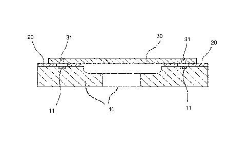
With reference to the drawings, a printhead manufactured
according to the method of the present invention has been
generally denoted as printhead 1.
The method according to the invention comprises a step of
providing a silicon substrate 10 including active ejecting
elements 11. Preferably, the active ejecting elements 11 are
heating elements: they heat the ink in order to cause generation
of ink droplets and ejection of the same through nozzles 31. In
this case, the printhead 1 is a thermal ink-jet printhead. In an
alternative embodiment, the active ejecting elements 11 are
piezoelectric elements that are electrically actuated in order
to displace a membrane and consequently push the ink out of the
nozzles 31, causing ejection of the same. In such embodiment,
the printhead 1 is a piezoelectric ink-jet printhead.
CA 02978137 2017-08-29
8
WO 2016/150715 PCT/EP2016/055126
The silicon substrate 10 may also include an electric circuit
(not shown) that is configured to properly and selectively
command the active ejecting elements 11 so that ink is ejected
on a determined medium to be printed, according to preset
patterns. The electric circuit can, however, also be located
elsewhere.
The method according to the invention further comprises a step
of providing a hydraulic structure layer 20 for defining
hydraulic circuits through which the ink flows which means that
it is configured to enable a guided flow of ink.
Preferably, the hydraulic structure layer 20 is a polymeric film
whose thickness can be comprised between lOpm and 200pm.
Further preferably, the hydraulic structure layer 20 defines
ejection chambers, in which the ink is subjected to the action
of the active ejecting elements 11, and feeding channels that
guide the ink to the ejection chambers. Preferably, the ink is
stored in a reservoir and reaches the feeding channels through
an ink feed slot (not shown).
The method according to the invention further comprises a step
of providing a silicon orifice plate 30 having a plurality of
nozzles 31 for ejection of the ink droplets.
Preferably, a plurality of silicon orifice plates 30 is obtained
from one silicon wafer 40 (see Fig. 9). After the nozzle
formation, the orifice plates 30 are separated from each other,
preferably through a dicing step. Subsequently, each orifice
plate 30 is aligned with and mounted on a respective silicon
substrate 10.
In the present context, the orifice plate 30 is preferably
obtained as briefly indicated here above. As shown in figure 1,
the silicon substrate 10, the hydraulic structure layer 20 and
the orifice plate 30 comprising the nozzles 31 are assembled, so
as to form the printhead 1. Preferably, the assembly step is
performed so that the hydraulic structure layer 20 is located
CA 02978137 2017-08-29
9
WO 2016/150715 PCT/EP2016/055126
between the silicon substrate 10 and the silicon orifice plate
30.
Preferably, the assembly step comprises a thermo-compression
sub-step, wherein the silicon substrate 10, the hydraulic
structure layer 20 and the orifice plate 30 are pressed
(pressure comprised, for example, between 1 bar and 10 bar) and,
at the same time, heated (temperature comprised, for example,
between 150 C and 200 C). The duration of the thermo-compression
sub-step can vary from a few minutes to a couple of hours. In
more detail, the orifice plate 30 can be obtained as follows.
A silicon-on-insulator wafer 40 is provided that has a
substantially planar extension delimited by a first surface 41
and a second surface 42 on opposite sides of the wafer 40. A
substantially planar extension is, in the context of the present
application, an extension which, in a thickness direction of the
wafer, does not deviate from a mathematical plane to an extent
of more than 5% of its largest lateral dimension. Preferably,
the first surface 41 and the second surface 42 comprise or,
preferably, consist of silicon oxide of a thickness of between
100 nm and up to a few microns, but also other materials could
be conveniently used for forming the first and second surfaces
41, 42 such as silicon nitride, silicon carbide and the like, or
a suitable photoresist material. Preferably, the first and
second surfaces 41, 42 are substantially parallel to each other,
which means that an angle between the first surface 41 and the
second surface 42 is 50 or less, preferably 1 or less.
The first and second surfaces 41, 42 are separated by a distance
D. The silicon-on-insulator wafer 40 can have a thickness of,
for example, between slightly above 100pm and up to 380pm.
Preferably, the silicon-on-insulator wafer 40 can be 200pm
thick.
In general, a silicon-on-insulator (SOI) wafer comprises three
different layers: a handle layer 37 made of silicon, a thickness
H of which usually ranges from 100 pm to 1000 pm, a device layer
38 made of silicon which is much thinner than the handle layer
37 and can have a thickness of as small as 1 pm or even slightly
CA 02978137 2017-08-29
WO 2016/150715 PCT/EP2016/055126
below. Further, the SOI comprises a buried insulating layer 39,
a thickness of which is usually up to a few microns, in between.
The insulator layer 39 can usually be made of silicon oxide but
also other insulating materials, such as silicon nitride or
silicon carbide, can be chosen for the insulator layer 39.
According to the invention, a thinning step is performed at the
second surface 42 of the silicon wafer 40. In this way, a
central portion 43 having a preset height H is removed. The
preset height H is equal to the thickness, or height, of the
handle layer 37 of the SOI wafer 40. Preferably, the height H
can be comprised between 100 pm and 360 pm. Particularly
preferably, the height H can be comprised between 120 pm and 160
pm.
After the thinning step, the silicon-on-insulator wafer 40 is
formed by a base portion 44, having a planar extension, and a
peripheral portion 45, that extends from the base portion 44
transversally with respect to the planar extension of the same
base portion 44. The shape of the silicon wafer 40 at this stage
is schematically shown in figure 9. Preferably, the outer
surface of the peripheral portion 45 extends from the base
portion 44 perpendicularly with respect to the planar extension
of the base portion 44.
In practice, after the thinning step, the silicon-on-insulator
wafer 40 has a ring structure as is illustrated for example in
figures 3f and 9. In other words, by means of the thinning step,
the thickness of the silicon-on-insulator wafer 40 is reduced,
apart from the peripheral portion 45, the thickness of which
remains substantially unchanged with respect to the initial
thickness of the silicon-on-insulator wafer 40. The silicon-on-
insulator wafer 40 thus shaped can be easily handled by hand
and/or by automatic systems in automated manufacturing lines due
to the relatively thick peripheral portion 45 and, at the same
time, can be used to obtain sufficiently thin orifice plates 30
from the inner part of the wafer 40. Accordingly, the peripheral
portion 45 can be used as a "handling portion".
CA 02978137 2017-08-29
11
WO 2016/150715 PCT/EP2016/055126
A plurality of through holes, each defining a respective nozzle
31 for ejection of the ink, is formed in the wafer 40.
As mentioned above, the orifice plate 30 is preferably obtained
through a dicing step wherein the silicon-on-insulator wafer 40,
after formation of the nozzles 31, is cut to obtain a plurality
of orifice plates. Figure 9 schematically shows how the silicon-
on-insulator wafer 40 includes a plurality of orifice plates 30.
Alternatively, the wafer 40 with the orifice plates 30 could be
directly joined to the hydraulic structure layer and silicon
substrate by means of a wafer bonding process. This wafer
bonding can be a direct bonding or an indirect bonding by means
of an adhesive layer.
Alternatively, the silicon device layer 38 of the silicon-on-
insulator wafer 40 for obtaining the orifice plates could be
separated from the handle layer 37 by wafer thinning after
temporary bonding of the device layer 38 to a further handle
substrate such as a wafer, tape or similar means. The temporary
bonding between the silicon-on-insulator wafer 40 and the handle
substrate could be obtained by a temporary bonding adhesive of
the thermal-release type or the solvent-release type. The final
thinning step could be realized both by silicon wet etching and
silicon dry etching or also by grinding or by chemical-
mechanical polishing, eventually completed with a silicon dry or
wet etching. The insulator layer 39 will guarantee the final
nozzle plate thickness.
In particular, the orifice plate 30 is obtained as a portion of
the base portion 44. Preferably, by means of the dicing step,
the orifice plate 30 is separated from other possible orifice
plates formed on the same silicon-on-insulator wafer 40, and
from the peripheral, or handling, portion 45.
Applying the proposed process flow starting from the device
layer of the silicon-on-insulator wafer 40, a device layer
thickness D1 can directly determine the final thickness of the
orifice plate obtained. More in detail, the device layer
thickness D1 which corresponds to the difference between the
aforementioned distance D, i.e. the distance between the first
CA 02978137 2017-08-29
12
WO 2016/150715 PCT/EP2016/055126
and second surfaces 41, 42, and the height H of the central
portion 43, i.e. the portion removed by means of the thinning
step, defines a longitudinal length L of the nozzles 31 of the
orifice plate 30.
In other terms, the longitudinal length L of the nozzles 31 is
substantially equal to the thickness of the base portion 44,
which is equal to the device layer thickness D1 of the SOI wafer
40. Without the use of the silicon-on-insulator wafer, this
would mean that the height H of the central portion 43 should be
determined so that, after the thinning step, the remaining base
portion 44 of the silicon wafer 40 has a thickness that defines
the longitudinal length L of the nozzles 31. While applying the
proposed method, the device layer thickness D1 of the silicon-
on-insulator wafer 40 can directly determine the final thickness
of the obtained orifice plate, thus avoiding the long lasting
thickness check procedure of the prior art. In fact, the
insulator layer 39 of the SOT wafer 40 acts as a stop layer for
the thinning process, due to the etching selectivity with
respect to an insulator material, in particular silicon oxide or
silicon dioxide.
Moreover, after the preferred subsequent step of removing the
insulator layer 39, the resulting silicon surface is free of
defects because the oxide etching process is in turn selective
with respect to the silicon so that the surface of the silicon
device layer acts as a stop layer for the mechanism removing the
insulator.
Advantageously, the thinning step can be performed by etching.
Preferably, the thinning etching step is a wet-etching step.
Alternatively, a reactive ion etching process or a dry-etching
process could be applied for the thinning step. In both cases,
the insulator layer process, due to the etching selectivity with
respect to a silicon oxide material.
Preferably, the thinning step comprises the following sub-steps:
- masking material deposition of at least the second surface
42; preferably, the masking is performed through an oxidation
process which is carried out on the whole silicon-on-insulator
CA 02978137 2017-08-29
13
WO 2016/150715 PCT/EP2016/055126
wafer 40. Thus, on at least the second surface 42, and
preferably on the whole silicon wafer 40, a layer of oxide is
formed;
- protection of an external ring on the second surface 42,
in particular on a peripheral zone, corresponding to the
peripheral portion 45 to be obtained; this protection could be
obtained by means of a photolithographic masking process, a
protective tape, or by using a wafer holder. It is to be noted
that the wafer holder may protect not only the mentioned
external ring, but also the wafer back side during the etching
of the masking material. Thus such etching is not necessarily of
the dry type, but it can be, under these circumstances, of the
wet type;
- removal of the portion of the masking material that is not
covered by the protection;
- removal, preferably by means of a wet-etching action, the
central portion 43, i.e. the portion of silicon wafer that is
not covered by the masking layer;
- at least partial removal of the masking material layer.
- at least partial removal of the buried oxide, i.e. the
insulator layer 39.
Alternatively, the thinning step can be performed by reactive
ion etching, dry etching, mechanical grinding or chemical-
mechanical polishing. In case of grinding, a grinding wheel
operated by a grinding machine provides the removal of the
central portion 43 without the need for any protection and/or
oxide layer. A polishing step is usually performed after the
grinding step to remove the grinding marks and the subsurface
cracks generated during the grinding step.
A preferred method further comprises a step of forming in the
device layer 38 of the silicon-on-insulator wafer 40 a plurality
of through holes, each defining a respective nozzle 31 for
ejection of the ink. Preferably the through holes are formed in
the base portion 44.
It has to be noted that, in the described preferred embodiments,
each nozzle 31 is formed before the thinning step. The nozzle
geometry should be selected in order to reduce the resistance to
CA 02978137 2017-08-29
14
WO 2016/150715 PCT/EP2016/055126
ink flow as well as to improve the uniformity of the nozzle
across the micro-electromechanical device.
Trapping of air can also be reduced or eliminated by nozzle
geometry. Preferably each nozzle 31 comprises a top portion 32
and a bottom portion 33, the latter being axially aligned to the
top portion 32. In the present context, "top" and "bottom" refer
to the position of the nozzle's portions with respect to the
printhead wafer on which the nozzle plate is mounted: the
"bottom" portion is closer to and directly facing the hydraulic
structure layer 20, whereas the "top" portion is farther from
the hydraulic structure layer 20.
The top cross section of the top portion 32 can he square,
circular or differently shaped.
The bottom portion 33 can have a rectangular or round top cross
section. Preferably the top portion 32 of each nozzle 31 has a
substantially cylindrical shape. Preferably the bottom portion
33 of each nozzle 31 has a substantially frusto-pyramidal shape.
The longitudinal length L of the nozzle 31 is defined by the
longitudinal length of the top portion 32 plus the height of the
bottom portion 33. Preferably the top portions 32 of the nozzles
31 of the orifice plate 30 are obtained by means of an etching
step that will be referred to as top portion etching step.
Preferably the top portion etching step is a dry-etching step.
In the described preferred embodiment, the top portion etching
step, preferably a dry-etching step, is carried out, wherein a
plurality of substantially cylindrical cavities 50 is formed in
the device layer 38 of the silicon-on-insulator wafer 40 at its
first surface 41. At least a part of each of the substantially
cylindrical cavities 50 defines the top portion 32 of a
respective nozzle 31. Each substantially cylindrical cavity 50
has a first longitudinal end 51 at the first surface 41 of the
silicon-on-insulator wafer 40, and a second longitudinal end 52
opposite to the first longitudinal end 51.
CA 02978137 2017-08-29
WO 2016/150715 PCT/EP2016/055126
Preferably the bottom portions 33 of the nozzles 31 of the
orifice plate 30 are obtained by means of an etching step that
will be referred to as bottom portion etching step.
Preferably the bottom portion etching step is an anisotropic
wet-etching step.
In the embodiments of Figs. 3, 4 and 5, the bottom portion
etching step, preferably an anisotropic wet-etching step, is
carried out, wherein a plurality of bottom portions 33,
preferably having a frusto-pyramidal shape, are formed at the
second end 52 of each of the substantially cylindrical cavities
50, thereby obtaining the nozzles 31 of the orifice plate 30, as
illustrated in Fig. 2.
In the embodiment of Figs. 6 and 7, the bottom portion etching
step, preferably an anisotropic wet-etching step, is carried
out, wherein a plurality of bottom portions 33, preferably
having a frusto-pyramidal shape, are formed at the first end 51
of each of the substantially cylindrical cavities 50, thereby
obtaining the nozzles 31 of the orifice plate 30, as illustrated
e. g. in Figs. 2 and 7h. Alternatively, as described in the
embodiment of Fig. 8, the nozzle 31 only comprises only a single
portion 34. In such a case the nozzles 31 preferably have a
frusto-pyramidal shape as described above in relation to the
bottom portion etching step. Preferably the nozzle etching step
is an anisotropic wet-etching step.
It has to be noted that both the top portion etching step, the
bottom portion etching step and the nozzle etching step
preferably include sub-steps of oxidation, masking, in
particular deposition of a photoresist film, removal of the
oxide not covered by the photoresist film, removal of the
silicon not covered by the oxide, and removal of the remaining
photoresist film and oxide. The method may also comprise a
masking step of the top portion etching step with a first mask
and a masking step of the bottom portion etching step with a
second mask, wherein both of the first and second masking steps
are carried out on the first surface. It is also possible that
an alignment of the top portion etching step and the bottom
CA 02978137 2017-08-29
16
WO 2016/150715 PCT/EP2016/055126
portion etching step is performed with a single mask on the
first surface.
These kinds of processes are known in the art and, therefore,
will not be disclosed in further detail.
In the embodiments of Figs. 3, 4 and 5, the thinning step is
carried out after the top portion etching step and before the
bottom portion etching step.
In the embodiment of Figs. 6 and 7, the thinning step is carried
out after the top portion etching step and the bottom portion
etching step. In the embodiment of Fig. 8, the thinning step is
carried out after the nozzle etching step.
In more detail, in the first embodiment illustrated in Fig. 3,
the longitudinal length of the substantially cylindrical
cavities 50 is substantially equal to the length of the top
portions 32 of the respective nozzles 31. Therefore the
longitudinal length of the substantially cylindrical cavities 50
is shorter than the thickness of the base portion 44, in other
words shorter than the thickness of the device layer 38.
In the second, fourth and fifth embodiments, illustrated in
Figs. 4, 6 and 7, respectively, the longitudinal length of the
substantially cylindrical cavities 50 is equal to the thickness
of the base portion 44, in other words equal to the thickness of
the device layer 38. In particular in the second embodiment,
this feature is advantageous because the top portion etching
step is performed at the first surface 41 of the SOT wafer 40,
and the bottom portion etching step is performed at the second
surface 42 of the SOI wafer. Thus the second end 52 of the
substantially cylindrical cavity 50 that is visible from the
second surface 42 through the insulator layer after the thinning
step can be used as a positional reference for a masking step of
the bottom portion etching step, so that the bottom portion 33
can be formed according to a proper alignment with the
respective top portion 32.
CA 02978137 2017-08-29
17
WO 2016/150715 PCT/EP2016/055126
In the fourth embodiment, illustrated in Fig. 6, this feature is
advantageous because the mask used in the bottom portion etching
step is aligned using a feature present on the same first
surface 41. Therefore, the substantially cylindrical cavity 50
has to be sufficiently long to be equal to the thickness of the
base portion 44, in other words equal to the thickness of the
device layer 38, in order to obtain an actual through hole.
In the fifth embodiment, illustrated in Fig. 7, this feature is
similarly advantageous because such an embodiment has the
further advantage of using only one mask for defining the top
and bottom portions on the same first surface 41. Therefore the
substantially cylindrical cavity 50 has to be sufficiently long.
Its length preferably is equal to the thickness of the base
portion 44 or, in other words, equal to the thickness of the
device layer 38, in order to obtain an actual through hole.
Preferably, as schematically shown in Fig 5, the method of
manufacturing an ink-jet printhead according to the third
embodiment comprises a forming step (Fig. 5b), wherein one or
more reference cavities 60, having a length equal to the
thickness of the base portion 44, in other words equal to the
thickness of the device layer 38, is formed at the first surface
41. In particular, the forming step is carried out before the
thinning step. Likewise, the longitudinal length of the
substantially cylindrical cavities 50 can be substantially equal
to the length of the top portion 32 of the nozzles 31. The
positional reference for the masking step included in the bottom
portion etching step is provided by the reference cavities 60
that are visible from the second surface 42 of the SOT wafer 40
through the silicon oxide layer, after the thinning step has
been carried out and before the bottom portion etching step is
carried out.
Preferably, after the nozzles 31 have been formed and the
thinning step has been carried out, the silicon wafer 40 is cut
in separate portions, each defining a respective orifice plate.
The orifice plate 30 of the printhead 1 will be one of the
orifice plates obtained from the silicon-on-insulator wafer 40.
CA 02978137 2017-08-29
18
WO 2016/150715 PCT/EP2016/055126
Alternatively, the silicon wafer with the nozzle plates could be
directly joined to the printhead wafer by means of a wafer
bonding process. This wafer bonding can be a direct bonding or
an indirect bonding by means of an adhesive layer.
It has to be noted that in many figures a couple of interruption
symbols 70 is present to indicate that the distance between the
nozzles 31 and the radially external portion 45 of the silicon
wafer 40 may be much greater than shown. In practice, a large
number of nozzles 31 are formed in the silicon wafer 40; for
sake of clarity, only a couple of them are shown in the
drawings.
FIRST EMBODIMENT
Figures 3a - 3g schematically show the basic method steps of the
first embodiment with the preferred process choice. In the first
embodiment, silicon oxide is used as masking layer on both
surfaces 41, 42 of the SOI wafer 40. In the method step of
figure 3a, a silicon-on-insulator wafer 40 is provided; a
silicon oxide layer 46 is formed on the external surface of the
silicon-on-insulator wafer 40, preferably through thermal
oxidation.
In the method step of Figure 3b, which shows an enlarged view of
an area of Fig. 3a, through a first lithographic process and
subsequent etching, preferably a dry etching, a plurality of
portions of silicon oxide are removed from the first surface 41.
Each area from which the oxide is removed will correspond to a
respective nozzle.
In the method step of Figure 3c, a silicon dry-etching process,
the "top portion etching step" referred to above, is performed
so that the substantially cylindrical cavities 50 are formed.
In this embodiment, the longitudinal length of the cylindrical
cavities 50 is substantially equal to the longitudinal length of
the top portions 32, preferably having a substantially
cylindrical shape, of the nozzles 31. Then, another oxidation
process is carried out so as to cover also the surface of the
substantially cylindrical cavities 50 with a layer of silicon
CA 02978137 2017-08-29
19
WO 2016/150715 PCT/EP2016/055126
oxide. In the method step of Figure 3d, an oxide etching is
performed in order to remove, from the second surface 42, a
central portion of oxide. The protection of the external ring
could be obtained by means of a photolithographic masking
process, a protective tape, or by using a wafer holder.
Preferably, this oxide etching process is performed by means of
wet-etching.
In the method step of Figure 3e, the "thinning step" is
performed, wherein the central portion 43 of the silicon-on-
insulator wafer 40 is removed acting on the second surface 42
through a silicon wet-etching, alternatively by grinding or dry
etching. As a consequence, the silicon-on-insulator wafer 40 is
now formed by the base portion 44 and the peripheral portion 45.
Another oxidation process is carried out, so that the sloping
surfaces 71 of the peripheral portion 45 are covered with a
layer of silicon oxide. In the method step of Figure 3f, through
a combination of lithographic process and oxide dry etching,
portions of oxide, the insulator layer 39 of the SOI, are
removed where the nozzles 31 are supposed to be formed, i.e. at
positions corresponding to the already formed substantially
cylindrical cavities 50.
In the method step of Figure 3g, a silicon anisotropic wet-
etching process, the "bottom portion etching step" mentioned
above, removes frusto-pyramidal portions of silicon where the
oxide, the insulator layer 39, has been removed so as to form
the bottom portions 33, preferably having a frusto-pyramidal
shape, of the nozzles 31. Later on, an oxide wet-etching is
performed in order to remove the layer of oxide that separates
each substantially cylindrical cavity 50 with the respective
bottom portion 33, preferably having a frusto-pyramidal shape,
and complete the formation of the nozzles 31. Finally, if
required, another oxidation step can be carried out, to cover
the whole structure with a layer of oxide.
SECOND EMBODIMENT
CA 02978137 2017-08-29
WO 2016/150715 PCT/EP2016/055126
Figures 4a to 4g schematically show the basic method steps of
the second embodiment. In the second embodiment, silicon oxide
is used as masking layer on both surfaces of the SOI wafer.
In the method step of Figure 4a, a silicon-on-insulator wafer 40
is provided. A silicon oxide layer 46 is formed on the external
surface of the silicon-on-insulator wafer 40, preferably through
thermal oxidation.
In the method step of Figure 4b, which shows an enlarged view of
a part of Fig. 4a, through a first lithographic process and
subsequent etching, preferably a dry etching, a plurality of
portions of silicon oxide is removed from the first surface 41.
Each area from which the oxide is removed will correspond to a
respective nozzle.
In the method step of Figure 4c, a silicon dry-etching process
is performed, the "top portion etching step" referred to above,
so that the substantially cylindrical cavities 50 are formed. In
this embodiment, a longitudinal length of the cylindrical
cavities 50 is substantially equal to the thickness of the base
portion 44, in other words equal to the thickness of the device
layer 38. Then, another oxidation method is carried out so as to
cover also the surface of the substantially cylindrical cavities
50 with a layer of silicon oxide 49.
In the method step of Figure 4d, an oxide etching is performed
in order to remove, from the second surface 42, a central
portion of oxide. The protection of the external ring could be
alternatively obtained by means of a photolithographic masking
method, by a protective tape or by using a wafer holder.
Preferably, this oxide etching process is performed by means of
wet-etching.
In the method step of Figure 4e, the "thinning step" is
performed, wherein the central portion 43 of the silicon-on-
insulator wafer 40 is removed, acting on the second surface 42
through a silicon wet-etching, alternatively by grinding or dry
etching. As a consequence, the silicon-on-insulator wafer 40 is
now formed by the base portion 44 and the peripheral portion 45.
CA 02978137 2017-08-29
21
WO 2016/150715 PCT/EP2016/055126
Further, another oxidation process is carried out, so that the
sloping surfaces 71 of the peripheral portions 45 are covered
with a layer of silicon oxide.
It has to be noted that the substantially cylindrical cavities
are now through holes that are visible also from the second
surface 42, through the buried oxide of the insulator layer 39.
This feature is advantageous because it provides a clear,
precise and reliable visual reference for the formation of the
frusto-pyramidal portions of the nozzles starting from the
backside, i.e. from the side of the second surface 42.
In the method step of Figure 4f, through a combination of
lithographic process and oxide dry etching, portions of oxide,
the oxide of the insulator layer 39, are removed where the
nozzles 31 are supposed to be formed, i.e. at positions
corresponding to the already formed substantially cylindrical
cavities 50. Further, a silicon anisotropic wet-etching process,
the "bottom portion etching step" mentioned above, removes
frusto-pyramidal portions of silicon where the oxide, the oxide
of the insulator layer 39, has been removed so as to form the
bottom portions 33 of the nozzles 31, preferably having a
frusto-pyramidal shape.
In the method step of figure 4g, an oxide wet-etching is
performed in order to remove the unnecessary oxide such as, for
example, the oxide left in the nozzles 31. Finally, if desired,
a further oxidation step can be carried out in order to cover
the whole structure with a layer of oxide.
THIRD EMBODIMENT
Figures 5a to 5g schematically show the basic method steps of
the third embodiment. In the third embodiment, silicon oxide is
used as masking layer on both surfaces of the SOI wafer. In the
method step of Figure 5a, a silicon-on-insulator wafer 40 is
provided. A silicon oxide layer 46 is formed on the external
surface of the silicon-on-insulator wafer 40, preferably through
thermal oxidation.
CA 02978137 2017-08-29
22
WO 2016/150715 PCT/EP2016/055126
In the method step of Figure 5b, through a first lithographic
process and subsequent oxide etching, preferably a dry etching,
and by a silicon etching method carried out on the first surface
41, a plurality of reference cavities 60 is formed.
Later on, an oxidation process is performed. The reference
cavities 60 will not be part of respective nozzles, but will be
used as a positional reference for the formation of the nozzles
31.
In the method step of Figure 5c, which shows an enlarged view of
a portion of Fig. 5b, through a second lithographic process,
aligned with the first, and subsequent etching, preferably a dry
etching process, a plurality of portions of silicon oxide 47 are
removed from the silicon oxide layer on the first surface 41.
Each area from which the oxide is removed will correspond to a
respective nozzle.
In the method step of Figure 5d, a silicon dry-etching process,
the "top portion etching step" referred to above, is performed
so that the substantially cylindrical cavities 50 are formed at
the first surface 41 that define the respective top portions 32,
preferably having a substantially cylindrical shape, of the
respective nozzle 31. In this embodiment, the longitudinal
length of the cylindrical cavities 50 is substantially equal to
the longitudinal length of the top portions 32, preferably
having a substantially cylindrical shape, of the nozzles 31.
Then, another oxidation process is carried out so as to cover
also the surface of the substantially cylindrical cavities 50
with a layer of silicon oxide 49.
In the method step of Figure 5e, an oxide etching is performed
in order to remove, from the second surface 42, a central
portion of oxide. The protection of the external ring could be
obtained by means of a photolithographic masking process, a
protective tape, or by using a wafer holder. Preferably, this
oxide etching process is performed by means of wet-etching.
In the method step of Figure 5f, the "thinning step" is
performed, wherein the central portion 43 of the silicon-on-
CA 02978137 2017-08-29
23
W02016/150715 PCT/EP2016/055126
insulator wafer 40 is removed acting on the second surface 42
through a silicon wet-etching process, alternatively by grinding
or dry etching. As a consequence, the silicon-on-insulator wafer
40 is now formed by the base portion 44 and the peripheral
portion 45.
In the method step of Figure 5g, another oxidation process is
carried out so that the sloping surfaces of the peripheral
portions 45 are covered with a layer of silicon oxide. It has to
be noted that, after the oxide wet-etching of the previous step,
the reference cavities 60 are now through holes that are visible
both from the first surface 41 and from the second surface 42.
Therefore, the reference cavities 60 can be used as positional
references for the remaining steps to be carried out for the
formation of the nozzles 31.
As described for the second embodiment, through a combination of
lithographic process and oxide dry etching, portions of oxide,
the oxide of the insulator layer 39, are removed where the
nozzles 31 are supposed to be formed, i.e. at positions
corresponding to the already formed substantially cylindrical
cavities 50. Later on, a sequence of lithographic process, oxide
dry etching and silicon anisotropic wet-etching is performed at
the lower surface 44a of the base portion 44 opposite to the
first surface 41.
Likewise, the bottom portions 33, preferably having a frusto-
pyramidal shape, of the nozzles 31 are formed, each of them
corresponding to a respective substantially cylindrical cavity
50.
Finally, an oxide wet-etching process removes the unnecessary
oxide such as, for example, the oxide left in the nozzles 31
and, if required, another oxidation step can be carried out in
order to cover the whole structure with a layer of oxide.
FOURTH EMBODIMENT
Figures 6a to 6i schematically show the basic method steps of
the fourth embodiment. In the fourth embodiment, silicon oxide
is used as masking layer on both surfaces of the SOI wafer. In
CA 02978137 2017-08-29
24
W02016/150715 PCT/EP2016/055126
the method step of Figure 6a, a silicon-on-insulator wafer 40 is
provided. A silicon oxide layer 46 is formed on the external
surface of the silicon-on-insulator wafer 40, preferably through
thermal oxidation.
In the method step of Figure 6b, which shows a zoomed area with
respect to Fig. 6a, through a first lithographic process and
subsequent etching, preferably a dry etching, a plurality of
portions of silicon oxide is removed from the first surface 41.
Each area from which the oxide is removed will correspond to a
respective nozzle.
In the method step of Figure 6c, a silicon dry-etching process,
the "top portion etching step" referred to above, is performed
so that the substantially cylindrical cavities 50 are formed. In
this embodiment, a longitudinal length of the cylindrical
cavities 50 is substantially equal to the thickness of the base
portion 44, in other words equal to the thickness of the device
layer 38.
Then, an oxidation process is carried out so as to cover also
the surface of the substantially cylindrical cavities 50 with a
layer of silicon oxide 49.
In the method step of Figure 6d, through a sequence of
lithographic process and oxide dry etching, portions of oxide
are removed around the substantially cylindrical cavities 50.
The cylindrical cavities 50 are protected, during this silicon
oxide dry etching process by a resist mask 48 applied during the
lithographic process described here above.
In the method step of Figure 6e, after the resist removal, an
anisotropic silicon wet-etching process, the above mentioned
"bottom portion etching step", forms the bottom portion 33,
preferably having a frusto-pyramidal shape, on the first surface
41 where, in the previous step, the oxide has been removed.
In the method step of Figure 6f, an oxide wet-etching process
removes the unnecessary oxide such as, for example, the oxide
CA 02978137 2017-08-29
WO 2016/150715 PCT/EP2016/055126
left in the nozzles 31 and an oxidation step is carried out, to
cover the whole structure with a new layer of oxide 91.
In the method step of Figure 6g, an oxide etching is performed
in order to remove, from the second surface 42, a central
portion of oxide. The protection of the external ring could be
obtained by means of a photolithographic masking process, a
protective tape or by using a wafer holder. Preferably, this
oxide etching process is performed by means of wet-etching.
In the method step of Figure 6h, the "thinning step" is
performed, wherein the central portion 43 of the silicon-on-
insulator wafer 40 is removed, acting on the second surface 42
through a silicon wet-etching, alternatively by grinding or dry
etching. As a consequence, the silicon-on-insulator wafer 40 is
now formed by the base portion 44 and the peripheral portion 45.
In the method step of Figure 61, an oxide wet-etching process
removes the not necessary oxide such as, for example, the oxide
left in the nozzles 31 and, if required, another oxidation step
can be carried out, to cover the whole structure with a new
layer of oxide 92.
FIFTH EMBODIMENT
Figures 7a to 71 schematically show the basic method steps of a
fifth embodiment. In the fifth embodiment, silicon oxide is used
as masking layer on both surfaces of the SOT wafer.
In the method step of Figure 7a, a silicon-on-insulator wafer 40
is provided. A silicon oxide layer 46, preferably having a
thickness of 1,400 nm, is formed on the external surface of the
silicon-on-insulator wafer 40, preferably through thermal
oxidation.
In the method step of Figure 7b, which shows an enlarged view of
a portion of Fig. 7a, through a first lithographic process and
subsequent etching, a plurality of portions 47 of silicon oxide
are removed from the first surface 41. A single mask is employed
to define the edges of the bottom portion and the top portion of
the nozzle. Each area from which the oxide is removed will
CA 02978137 2017-08-29
26
WO 2016/150715 PCT/EP2016/055126
correspond to a respective nozzle. About half of the thickness
of the silicon oxide layer, e. g. about 700 nm, is removed in
this method step. Preferably the oxide etching in the method
step of Figure 7b is performed by means of dry-etching.
In the method step of Figure 7c, through a second lithographic
process, the silicon oxide layer is covered with a positive
photoresist 48, which is then exposed and developed, leaving
uncovered the portion of oxide corresponding to the top portion
of the nozzle 90.
In the method step of Figure 7d, etching of the silicon oxide
portion exposed after step 7c is performed, completely removing
the silicon oxide in the area corresponding to the nozzle and
reducing the thickness, e. g. to about 700 nm, in the area
around it. Preferably the oxide etching in step 7d is performed
by means of dry-etching.
In the method step of Figure 7e, a silicon dry-etching process,
the "top portion etching step" referred to above, is performed
so that the substantially cylindrical cavities 50 are formed.
The oxide of the insulator layer 39 of the silicon-on-insulator
wafer 40 in use acts as a stop etching layer during the
cylindrical cavities dry etch step.
A longitudinal length of the substantially cylindrical cavities
50 is substantially equal to the thickness of the future base
portion 44, in other words equal to the thickness of the device
layer 38. After that, a silicon oxide layer 49, preferably
having a thickness of 140 nm, is formed on the walls of the
substantially cylindrical cavities 50, preferably through
thermal oxidation.
In the method step of Figure 7f, through a third lithographic
process, the silicon oxide layer is covered with a negative
photoresist 53, which is then exposed and developed, in order to
cover the portion corresponding to the substantially cylindrical
cavities 50 and leaving uncovered the remaining portion of the
silicon oxide layer. The coating can be provided by deposition
CA 02978137 2017-08-29
27
W02016/150715 PCT/EP2016/055126
of a negative photoresist dry-film, or by spray coating of a
liquid negative photoresist.
In the method step of Figure 7g, the etching of the silicon
oxide portion, exposed in the previous step, is performed,
completely removing the silicon oxide in the area 54
corresponding to the edges of the nozzle bottom portion 33 and
reducing the thickness e. g. to about 700 nm in the area around
it. Preferably, the oxide etching described in Fig. 7g, is
performed by means of dry-etching. After that, the photoresist
is removed.
In the method step of Figure 7h, an anisotropic silicon wet-
etching process, the above mentioned "bottom portion etching
step", forms the bottom portions 33, preferably having a
substantially frusto-pyramidal shape, where the oxide has been
removed in the previous method step.
In the method step of Figure 7i, zoomed out to the original
wafer area, the etching of the silicon oxide is performed,
completely removing the silicon oxide layers, back and front of
the wafer, including the oxide left inside the nozzles 31.
Preferably, this oxide etching method is performed by means of
wet-etching. Later on, a new silicon oxide layer 91, preferably
having a thickness of 140 nm, is formed on the whole surface,
preferably through thermal oxidation.
In the method step of Figure 7j, an oxide etching is performed
in order to remove, from the second surface 42, a central
portion of oxide. The protection of the external ring could be
obtained by means of a photolithographic masking process, a
protective tape or by using a wafer holder. Preferably, this
oxide etching process is performed by means of wet-etching.
In the method step of Figure 7k, the "thinning step" is
performed, wherein the central portion 43 of the silicon-on-
insulator wafer 40 is removed acting on the second surface 42
through a silicon wet-etching (alternatively by grinding or dry
etching). As a consequence, the silicon-on-insulator wafer 40 is
now formed by the base portion 44 and the peripheral portion 45.
CA 02978137 2017-08-29
28
W02016/150715 PCT/EP2016/055126
In the method step of Figure 71, an oxide wet-etching process
completely removes all the oxide layers on the silicon-on-
insulator wafer 40. In particular, it also removes the oxide of
the insulator layer 39 and thus creates the openings in the
nozzle top portions. Finally, if required, a final oxidation
process can be performed to provide a new oxide layer 92.
SIXTH EMBODIMENT
Figures 8a to 8g schematically show the basic method steps of
the sixth embodiment. In the sixth embodiment, silicon oxide is
used as masking layer on both surfaces of the SC)I wafer.
In the method step of Figure 8a, a silicon-on-insulator wafer 40
is provided. A silicon oxide layer 46 is formed on the external
surface of the silicon-on-insulator wafer 40, preferably through
thermal oxidation.
In the method step of Figure 8b, which shows an enlarged view of
a portion of Fig. 8a, through a lithographic process and
subsequent etching, preferably a dry etching, a plurality of
portions of silicon oxide 47 are removed from the first surface
41. Each area from which the oxide is removed will correspond to
a respective nozzle.
In the method step of Figure 8c, an anisotropic silicon wet-
etching process forms the single portion 34, preferably having a
substantially frusto-pyramidal shape, where, in the previous
step, the oxide has been removed. In this step the pyramid base
width is chosen so that the final height of the pyramid or
frusto-pyramid is equal to the silicon device thickness 38.
In the method step of Figure 8d (zoomed out to the original
wafer area), an oxide wet etching is performed in order to
remove from both the first surface 41 and the second surface 42,
the silicon oxide. After that, a new silicon oxide layer 91,
preferably having a thickness of 140 nm, is formed on the whole
surface, preferably through thermal oxidation.
CA 02978137 2017-08-29
29
WO 2016/150715 PCT/EP2016/055126
In the method step of Figure 8e, an oxide etching is performed
in order to remove, from the second surface 42, a central
portion of oxide. The protection of the external ring could be
obtained by means of a photolithographic masking process, a
protective tape or by using a wafer holder. Preferably, this
oxide etching process is performed by means of wet-etching.
In the method step of Figure 8f, the "thinning step" is
performed, wherein the central portion 43 of the silicon-on-
insulator wafer 40 is removed acting on the second surface 42
through a silicon wet-etching, alternatively by grinding or dry
etching. As a consequence, the silicon-on-insulator wafer 40 is
now formed by the base portion 44 and the peripheral portion 45.
In the method step of Figure 8g, an oxide wet-etching process
removes the unnecessary oxide and finally, if desired, a further
oxidation step can be carried out to provide a new oxide layer
92.