Note: Descriptions are shown in the official language in which they were submitted.
Description
Title of Invention: SEMICONDUCTOR LASER LIGHT SOURCE DEVICE,
SEMICONDUCTOR LASER LIGHT SOURCE SYSTEM, AND IMAGE DISPLAY
APPARATUS
Technical Field
[0001] The
present invention relates to a semiconductor laser light source device and a
semiconductor laser light source system each including a cooler that cools a
semiconductor laser, and to an image display apparatus including the
semiconductor laser
light source device or the semiconductor laser light source system.
Background Art
[0002] In
recent years, solid-state light sources such as LEDs or semiconductor lasers
have been widely commercially available or suggested as light sources for
large
high-brightness projectors intended for large halls or digital cinemas, for
small to medium
sized projectors intended mainly for a small number conference or
presentation, and for
projection monitors including, in its casing, a projection optical system and
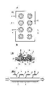
a large screen.
In these devices, the conventional lamps used as the light sources for many
projectors and
projection monitors are replaced by the solid-state light sources.
Accordingly, these
devices have advantages of, for example, wider color gamut, instant light
capability, low
power consumption, and long life.
[0003]
Particularly, the semiconductor lasers have additional advantages of higher
brightness and higher output through superposition of light. Thus,
high-output
semiconductor laser light source devices using a larger number of
semiconductor lasers
are being developed for use in large high-brightness projectors that project
large screens.
[0004] However, the semiconductor lasers are more heat-sensitive than the
other
CAN_DMS. \108852900\2
CA 2979520 2017-09-27
2
solid-state light sources such as LEDs, and the electrical-to-optical
efficiency thereof is
prone to extremely decrease according to increase in temperature of the
elements.
Furthermore, the continued emission of high-output light at high temperatures
expedites
degradation of the elements and tends to shorten the life thereof. Thus,
the
semiconductor lasers require a heat dissipation structure with cooling
capability higher
than those of the other solid-state light sources to obtain a desired amount
of light even
when the ambient temperature is high.
[0005] For
example, Patent Document I discloses a structure including rectangular tine
shaped radiating fins placed on a base equipped with a semiconductor laser,
and a cooling
fan fixed to the radiating fins with a driving substrate having holes
interposed
therebetween.
[0006] Furthermore, Patent Document 2 discloses a structure in which a
flexible
substrate for electrically connecting semiconductor lasers is embedded in a
heat transfer
component or in a base of a heat sink to dissipate heat from the semiconductor
lasers.
Prior-Art Documents
Patent Documents
[0007] Patent Document 1: Japanese Patent Application Laid-Open No. 2001-
326411
Patent Document 2: Japanese Patent Application Laid-Open No. 2011-76781
Summary of Invention
Problems to be Solved by the Invention
[0008] In
the structure disclosed by Patent Document 1, the radiating fins formed to
cool the semiconductor lasers are cooled by the cooling fan through the
driving substrate
having the holes. Since the driving substrate blocks winds blown by the
cooling fan,
CAN_DMS: \10885290012
CA 2979520 2017-09-27
3
there have been problems with inefficient cooling of the radiating fins,
decrease in the
cooling capability, and inefficient cooling of the semiconductor lasers.
[0009] In the structure disclosed by Patent Document 2, when the flexible
substrate
that electrically connects the semiconductor laser and the heat sink is placed
therebetween,
the contact area between the heat sink and the semiconductor laser that is a
heat
generating source is reduced. Accordingly, increase in thermal resistance
reduces the
cooling capability, thus posing a problem with inefficient cooling of the
semiconductor
laser.
[0010] To this end, the present invention has an object of providing a
technique that
allows a semiconductor laser to be efficiently cooled.
Means to Solve the Problems
[0011] A semiconductor laser light source device according to the present
invention
includes: a semiconductor laser; a cooler that cools the semiconductor laser;
and a
driving substrate that drives the semiconductor laser, wherein the cooler is
placed in
contact with a surface of the semiconductor laser, the surface being opposite
to a light
emitting surface of the semiconductor laser, the driving substrate is placed
in contact with
a surface of the cooler, the surface being opposite to a surface of the cooler
on which the
semiconductor laser is placed, and the cooler includes a hollow in which a
plurality of
fins are arranged.
[0012] A semiconductor laser light source device according to the present
invention
includes: a semiconductor laser; a cooler that cools the semiconductor laser;
and a
driving substrate that drives the semiconductor laser, wherein each of the
cooler and the
driving substrate is placed in contact with a surface of the semiconductor
laser, the
surface being opposite to a light emitting surface of the semiconductor laser,
the cooler is
formed in a protruding shape so that a center of the cooler in a width
direction is higher
CAN_DMS \108852900\2
CA 2979520 2017-09-27
4
than ends of the cooler, or is formed in a depressed shape so that the center
of the cooler
in the width direction is lower than the ends of the cooler, and a plurality
of fins are
arranged on a lower surface of the cooler.
[0013] A semiconductor laser light source system according to the present
invention
includes a plurality of the semiconductor laser light source devices.
[0014] An image display apparatus according to the present invention includes
the
semiconductor laser light source device or the semiconductor laser light
source system.
Effects of the Invention
[0015] According to the present invention, since a semiconductor laser and a
cooler are
in direct contact with each other, the thermal resistance between the
semiconductor laser
and the cooler can be reduced, and the semiconductor laser can be efficiently
cooled.
[0016] The objects, features, aspects and advantages of the present
invention will
become more apparent from the following detailed description and the
accompanying
drawings of the present invention.
Brief Description of Drawings
[0017] FIG. 1 illustrates a structure of an image display apparatus
including
semiconductor laser light source devices according to Embodiment 1.
FIGS. 2A to 2C illustrate an outline structure of the semiconductor laser
light source
device according to Embodiment 1.
FIGS. 3A to 3C illustrate a structure of a semiconductor laser according to
Embodiment
1.
FIG. 4 illustrates an outline structure of a semiconductor laser light source
system
according to Embodiment 1.
CAN_DMS \108852900\2
CA 2979520 2017-09-27
5
FIGS. 5A to 5C illustrate an outline structure of a semiconductor laser light
source device
according to Embodiment 2.
FIGS. 6A to 6C illustrate a structure of a semiconductor element according to
Embodiment 2.
FIGS. 7A to 7C illustrate another outline structure of the semiconductor laser
light source
device according to Embodiment 2.
FIG. 8 illustrates an outline structure of a semiconductor laser light source
system
according to Embodiment 2.
FIGS. 9A to 9C illustrate an outline structure of a semiconductor laser light
source device
according to Embodiment 3.
FIGS. 10A to 10C illustrate another outline structure of the semiconductor
laser light
source device according to Embodiment 3.
FIGS. 11A to 11C illustrate another outline structure of the semiconductor
laser light
source device according to Embodiment 3.
FIGS. 12A to 12C illustrate another outline structure of the semiconductor
laser light
source device according to Embodiment 3.
Description of Embodiments
[0018] [Embodiment 1]
Embodiment 1 according to the present invention will be hereinafter described
with reference to the drawings. Semiconductor laser light source devices 100,
a
semiconductor laser light source system 200, and an image display apparatus
300
according to Embodiment 1 will be described in detail. First, the image
display
apparatus 300 will be described. FIG. 1 illustrates a structure of the image
display
apparatus 300 according to Embodiment I.
CAN_DMS' \108852900\2
CA 2979520 2017-09-27
6
[0019] The image display apparatus 300 includes the semiconductor laser light
source
devices 100 of three types that are red, blue, and green, an illumination
optical system
101, an image display system 102, and a projection optical system 103. The
semiconductor laser light source devices 100 are high-output semiconductor
laser light
source devices each including semiconductor lasers.
[0020] The
illumination optical system 101 combines and converts the red, blue, and
green lights emitted by the semiconductor laser light source devices 100 into
white light,
and emits the white light to the image display system 102. For example,
digital light
processing (DLP) or liquid crystal on silicon (LCOS) can be used as the image
display
system 102. The image produced by the image display system 102 is enlarged by
the
projection optical system 103, and displayed on a screen 104.
[0021]
Although the image display apparatus 300 in FIG. 1 is intended to represent a
projector that displays white light by combination with the semiconductor
laser light
source devices 100 of three types that are red, blue, and green, it may be an
image display
apparatus that displays white light by combination with a semiconductor laser
and a
phosphor or by combination with a semiconductor laser and an LED.
[0022] Next, the semiconductor laser light source device 100 according to
Embodiment
I will be described. FIGS. 2A to 2C illustrate an outline structure of the
semiconductor
laser light source device 100. Specifically, FIG. 2A is a plan view of the
semiconductor
laser light source device 100, FIG. 2B is a cross-sectional view taken along A-
A of FIG.
2A, and FIG. 2C is a side view of the semiconductor laser light source device
100.
FIGS. 3A to 3C illustrate a structure of a semiconductor laser 1.
Specifically, FIG. 3A is
a plan view of the semiconductor laser 1, FIG. 3B is a cross-sectional view
taken along
the line B-B of FIG. 3A, and FIG. 3C is a cross-sectional view taken along the
line C-C of
FIG. 3A.
CAN_DMS \108852900\2
CA 2979520 2017-09-27
7
[0023] As illustrated in FIGS. 2A to 2C, the semiconductor laser light
source device
100 includes the (for example, eight) semiconductor lasers 1, a cooler 2, and
a driving
substrate 3. First, the semiconductor laser 1 will be described.
[0024] As illustrated in FIGS. 3A to 3C, the semiconductor laser 1
includes a chip 11,
a light emitting layer 12, a heat dissipation block 13, a plate 14, terminal
pins 15, a
package 16, and a glass window 17. The light emitting layer 12 is a layer that
emits
light, and is formed in the chip 11. Since the chip 11 generates heat, it is
placed on the
side surface of the heat dissipation block 13 and above the plate 14, and
dissipates heat
into the heat dissipation block 13. The terminal pins 15 are components that
are
supplied with power from outside and bring the chip 11 into conduction to
allow the chip
11 to emit light. The terminal pins 15 are connected to the chip ii through a
wire 18.
Since the performance of the chip 11 is degraded by influence of, for example,
dust, the
chip 11 is sealed by the package 16 while it is placed above the plate 14
through the heat
dissipation block 13. Accordingly, the influence of, for example, dust is
eliminated.
The glass window 17 is placed on the upper surface of the package 16, and
transmits the
light emitted from the light emitting layer 12. The emitted light is
illustrated by arrows
in FIGS. 3A to 3C. The same holds true for the other drawings.
[0025] As illustrated in FIGS. 2A to 2C, the cooler 2 is a component for
cooling the
semiconductor lasers 1. The semiconductor lasers 1 are arranged in two lines
on the
upper surface of the cooler 2 so that the heat dissipation blocks 13 on each
of which the
chip 11 is placed are facing to each other. The cooler 2 is placed in contact
with the
lower surfaces of the semiconductor lasers 1 (surfaces of the semiconductor
lasers 1 that
are opposite to light emitting surfaces thereof), and is placed directly below
the heat
dissipation blocks 13. The driving substrate 3 is a substrate equipped with a
driving
circuit for driving the semiconductor lasers 1. The driving substrate 3 is
placed in
CAN_DMS= \108852900\2
CA 2979520 2017-09-27
8
contact with the lower surface of the cooler 2 (surface opposite to a surface
on which the
semiconductor lasers 1 are arranged).
[0026] The cooler 2 includes a hollow 2a in which fins 7 are arranged, and
through
holes 2b into which the terminal pins 15 are inserted. The hollow 2a is formed
at the
center of the cooler 2 in its width direction along the longitudinal direction
and placed
below the heat dissipation blocks 13, and the fins 7 are arranged below the
heat
dissipation blocks 13. The cooler 2 functions as a liquid cooling device, by
causing, for
example, water to flow through the cooler 2 using the fins 7 as a channel. The
channel
is illustrated by open arrows in FIGS. 2A to 2C. The same holds true for the
other
drawings.
[0027] The through holes 2b are formed in respective positions of the terminal
pins 15
of the semiconductor lasers 1. Although not illustrated, through holes into
which the
terminal pins 15 are inserted are also formed in the driving substrate 3.
[0028] Next, the semiconductor laser light source system 200 will be
described. FIG.
4 illustrates an outline structure of the semiconductor laser light source
system 200. As
illustrated in FIG. 4, the semiconductor laser light source system 200
includes the (for
example, three) semiconductor laser light source devices 100 horizontally
arranged.
Although FIG. 4 illustrates the structure in which each of the semiconductor
laser light
source devices 100 includes the cooler 2, the semiconductor lasers 1 of the
three
semiconductor laser light source devices 100 may be placed on the one cooler
2.
Furthermore, although the image display apparatus 300 in FIG. 1 includes the
three
semiconductor laser light source devices 100, it may include the three
semiconductor
laser light source systems 200 instead.
[0029] As described above, in the semiconductor laser light source device 100
according to Embodiment 1, the cooler 2 is placed in contact with the surfaces
of the
CAN_DMS: \ 108852900 12
CA 2979520 2017-09-27
9
semiconductor lasers 1 that are opposite to the light emitting surfaces
thereof, and the
driving substrate 3 is placed in contact with the surface of the cooler 2 that
is opposite to
the surface on which the semiconductor lasers I are arranged.
[0030] Since the semiconductor lasers 1 and the cooler 2 are in direct
contact with each
other, the thermal resistance between the semiconductor lasers 1 and the
cooler 2 can be
reduced, and the semiconductor lasers 1 can be efficiently cooled. With
efficient
cooling of the semiconductor lasers 1, not only the semiconductor lasers 1 but
also the
semiconductor laser light source devices 100 can be used for a longer period
of time.
[0031] Furthermore, since the semiconductor laser light source system 200
includes the
semiconductor laser light source devices 100, it can produce higher output
than that by
the semiconductor laser light source device 100 alone.
[0032] Furthermore, since the image display apparatus 300 includes the
semiconductor
laser light source devices 100, it can efficiently cool the semiconductor
lasers 1.
Alternatively, when the image display apparatus 300 includes the semiconductor
laser
.. light source system 200, besides the advantage above, it can produce an
advantage of
higher output than that when it includes the semiconductor laser light source
devices 100.
[0033] [Embodiment 2]
Next, a semiconductor laser light source device 110 according to Embodiment 2
will be described. FIGS. SA to SC illustrate an outline structure of the
semiconductor
laser light source device 110 according to Embodiment 2. Specifically, FIG. 5A
is a
plan view of the semiconductor laser light source device 110, FIG. 513 is a
cross-sectional
view taken along E-E of FIG. SA, and FIG. SC is a cross-sectional view taken
along F-F
of the semiconductor laser light source device 110. FIGS. 6A to 6C illustrate
a structure
of a semiconductor element 4. Specifically, FIG. 6A is a plan view of the
semiconductor element 4, FIG. 6B is a cross-sectional view taken along G-G of
FIG. 6A,
CAN_DMS \10885290012
CA 2979520 2017-09-27
10
and FIG. 6C is a cross-sectional view taken along H-H of FIG. 6A. The same
reference
numerals as those according to Embodiment 1 will be assigned to the same
constituent
elements and the description thereof will be omitted in Embodiment 2.
[0034] As illustrated in FIGS. 5A to 5C, the semiconductor laser light
source device
.. 110 includes the semiconductor elements 4, the cooler 2, and the driving
substrate 3. As
illustrated in FIGS. 6A to 6C, the semiconductor element 4 is a large
semiconductor
element in which the (for example, two) chips 11 are placed on the respective
heat
dissipation blocks 13. The semiconductor element 4 includes the (for example,
two)
chips 11, the (for example, fourteen) light emitting layers 12, the (for
example, two) heat
dissipation blocks 13, the plate 14, the terminal pins 15, the package 16, and
the glass
window 17. The semiconductor elements 4 are arranged on the upper surface of
the
cooler 2, and the two heat dissipation blocks 13 in each of the semiconductor
elements 4
are arranged to face to each other.
[0035] The seven light emitting layers 12 are arranged per the chip 11. The
two heat
.. dissipation blocks 13 in each of the semiconductor elements 4 are arranged
so that the
seven light emitting layers 12 arranged in one of the two heat dissipation
blocks 13 face
to the seven light emitting layers 12 arranged in the other of the heat
dissipation blocks 13.
The arrangement direction of the light emitting layers 12 is parallel to the
width direction
of the cooler 2. Furthermore, the arrangement direction of the two
semiconductor
elements 4 is vertical to the arrangement direction of the light emitting
layers 12. Thus,
the channel of the fins 7 is parallel to the longitudinal direction of the
cooler 2, that is, the
arrangement direction or the two semiconductor elements 4.
[0036] Since the chips 11 of each of the semiconductor elements 4 include
the light
emitting layers 12, they are larger than those of the semiconductor lasers 1
according to
Embodiment 1. Furthermore, the heat dissipation blocks 13 for cooling the
chips 11 and
CAN_DMS \108852900\2
CA 2979520 2017-09-27
11
the plates 14 are similarly larger. The cooler 2 is placed directly below the
heat
dissipation blocks 13 to be in contact with the semiconductor elements 4.
[0037] The terminal pins 15 are arranged outside of the heat dissipation
blocks 13.
As a result, the two heat dissipation blocks 13 can be closely placed.
Furthermore, with
the terminal pins 15 placed outside of the heat dissipation blocks 13, the
cooler 2 can be
placed directly below the heat dissipation blocks 13 to be in contact with the
semiconductor elements 4 similarly as in the Embodiment 1. As a result, since
the
thermal resistance between the heat dissipation blocks 13 and the cooler 2 can
be reduced,
the semiconductor elements 4 can be efficiently cooled.
[0038] Furthermore, since the number of the terminal pins 15 in the
semiconductor
laser light source device 110 can be reduced more than that of the
semiconductor laser 1
according to Embodiment 1 by including the semiconductor elements 4 in each of
which
the chips 11 including the light emitting layers 12 are placed, a heat
dissipation area of the
semiconductor laser light source device 110 can be relatively increased.
Accordingly,
the semiconductor elements 4 can be efficiently cooled.
[0039] Next, another structure according to Embodiment 2 will be described.
FIGS.
7A to 7C illustrate another outline structure of the semiconductor laser light
source device
according to Embodiment 2. Specifically, FIG. 7A is a plan view of a
semiconductor
laser light source device 120, FIG. 7B is a cross-sectional view taken along
the line I-I of
FIG. 7A, and FIG. 7C is a cross-sectional view taken along the line J-J of
FIG. 7A.
[0040] The arrangement direction of the two semiconductor elements 4 is
vertical to
the arrangement direction of the light emitting layers 12 in the structure of
FIGS. 5A to
5C. As a result, one channel can be formed per the semiconductor element 4. In
contrast, the arrangement direction of the two semiconductor elements 4 is
parallel to the
arrangement direction of the light emitting layers 12 in the structure of
FIGS. 7A to 7C.
CAN_DMS' M08852900\2
CA 2979520 2017-09-27
12
In other words, the semiconductor elements 4 are arranged so that the
arrangement
direction of the seven light emitting layers 12 is parallel to the
longitudinal direction of
the cooler 2. Thus, since the channel of the fins 7 is formed in parallel with
the width
direction of the cooler 2 and does not pass through the semiconductor elements
4, an
advantage that each temperature of the semiconductor elements 4 can be
controlled is
obtained.
[0041] Next, a semiconductor laser light source system 201 according to
Embodiment
2 will be described. FIG. 8 illustrates an outline structure of the
semiconductor laser
light source system 201. As illustrated in FIG. 8, the semiconductor laser
light source
system 201 includes the (for example, three) semiconductor laser light source
devices 110
horizontally arranged. Although FIG. 8 illustrates the structure in which each
of the
semiconductor laser light source devices 110 includes the cooler 2, the
semiconductor
elements 4 of the three semiconductor laser light source devices 110 may be
placed on the
one cooler 2.
[0042] Furthermore, the semiconductor laser light source system 201 may
include the
semiconductor laser light source devices 120 horizontally arranged instead of
the
semiconductor laser light source devices 110. Furthermore, although the image
display
apparatus 300 in FIG. 1 includes the three semiconductor laser light source
devices 100, it
may include the three semiconductor laser light source systems 201 instead.
[0043] Thus, in the semiconductor laser light source devices 110 and 120
according to
Embodiment 2, the semiconductor laser is the semiconductor element 4 in which
the
chips 11 are arranged on the respective heat dissipation blocks 13, and the
cooler 2 is
placed directly below the heat dissipation blocks 13 to be in contact with the
semiconductor elements 4. Thus, since the number of the terminal pins 15 can
be
reduced more than that according to Embodiment 1, the contact area between the
cooler 2
CAN_DMS \10885290012
CA 2979520 2017-09-27
13
and the semiconductor elements 4 can be increased, and the semiconductor
elements 4
can be more efficiently cooled.
[0044] Accordingly, since the number of the terminal pins 15 can be reduced
more
than that according to Embodiment 1, the semiconductor laser light source
devices 110
and 120 can be downsized.
[0045] Since the semiconductor laser light source system 201 includes the
semiconductor laser light source devices 110 or 120, it can produce higher
output than
that by the semiconductor laser light source device 110 or 120 alone.
[0046] Furthermore, since the light source itself can be downsized, the
image display
apparatus 300 that is higher in reliability and smaller can be obtained.
[0047] [Embodiment 3]
Next, a semiconductor laser light source device 130 according to Embodiment 3
will be described. FIGS. 9A to 9C illustrate an outline structure of the
semiconductor
laser light source device 130 according to Embodiment 3. Specifically, FIG. 9A
is a
plan view of the semiconductor laser light source device 130, FIG. 9B is a
cross-sectional
view taken along the line K-K of FIG. 9A, and FIG. 9C is a side view of the
semiconductor laser light source device 130. The same reference numerals as
those
according to Embodiments 1 and 2 will be assigned to the same constituent
elements and
the description thereof will be omitted in Embodiment 3.
[0048] Although the driving substrate 3 is placed in contact with the lower
surface of
the cooler 2 (surface that is opposite to the surface of the cooler 2 on which
the
semiconductor lasers 1 are arranged) in Embodiment 1, each of the cooler 2 and
the
driving substrate 3 is placed in contact with the surface of the semiconductor
laser 1 that
is opposite to the light emitting surface thereof in Embodiment 1
[0049] As illustrated in FIGS. 9A to 9C, the semiconductor lasers 1 are
arranged in two
CAN_DMS 1108852900\2
CA 2979520 2017-09-27
14
lines so that the heat dissipation blocks 13 are facing to each other. The
cooler 2 is
formed in a protruding shape so that its center in the width direction is
higher than the
ends and that the upper surface at the center in the width direction is placed
in contact
with inner portions of the lower surfaces of the plates 14 of the
semiconductor lasers 1.
.. The driving substrate 3 is divided into two which are placed in contact
with respective
outside portions of the lower surfaces of the plates 14. The pair of the
driving substrates
3 is placed above both ends of the cooler 2 in the width direction, and is not
in contact
with the cooler 2. The terminal pins 15 are arranged to protrude downward from
pairs of
the driving substrates 3. In other words, the terminal pins 15 are arranged at
both ends
.. of the semiconductor laser light source device 130 in the width direction,
and the cooler 2
is arranged between the terminal pins 15 arranged at both ends of the
semiconductor laser
light source device 130 in the width direction.
[0050] The cooler 2 in Embodiment 3 differs from that in Embodiment 1 in that
it
include neither the hollow 2a nor the through holes 2b and the fins 7 are
arranged on the
lower surface of the cooler 2. Furthermore, a fan 8 is placed on the back of
the Ens 7.
[0051] Next, another outline structure of the semiconductor laser light
source device
according to Embodiment 3 will be described. FIGS. 10A to 10C illustrate
another
outline structure of the semiconductor laser light source device according to
Embodiment
3. Specifically, FIG. 10A is a plan view of a semiconductor laser light source
device
140, FIG. 10B is a cross-sectional view taken along L-L of FIG. 10A, and FIG.
10C is a
side view of the semiconductor laser light source device 140.
[0052] As illustrated in FIGS. 10A to 10C, the semiconductor lasers 1 are
arranged in
two lines so that the chips 11 including the light emitting layer 12 are
facing to each other.
The terminal pins 15 are arranged at the center of the semiconductor laser
light source
device 140 in the width direction. The driving substrate 3 is placed at the
center of the
CAN_DMS: \108852900\2
CA 2979520 2017-09-27
15
semiconductor laser light source device 140 in the width direction, and both
ends of the
upper surface of the driving substrate 3 in the width direction are placed in
contact with
inner portions of the lower surfaces of the plates 14 of the semiconductor
lasers 1. The
cooler 2 is formed in a depressed shape so that its center in the width
direction is lower
than the ends and that both ends of the upper surface in the width direction
are placed in
contact with respective outside portions of the lower surfaces of the plates
14 of the
semiconductor lasers 1.
[0053] Next, two outline structures with the semiconductor elements 4 as the
other
outline structures of the semiconductor laser light source device according to
Embodiment 3 will be described. FIGS, 11A to 11C illustrate another outline
structure
of the semiconductor laser light source device according to Embodiment 3.
Specifically,
FIG. 11A is a plan view of a semiconductor laser light source device 150, FIG.
11B is a
cross-sectional view taken along M-M of FIG. 11A, and FIG. 11C is a cross-
sectional
view taken along N-N of FIG. 11A.
[0054] As illustrated in FIGS. 11A to 11C, the semiconductor laser light
source device
150 includes the semiconductor elements 4 each including the terminal pins 15
placed
outside of the heat dissipation block 13, and the cooler 2 between the
terminal pins 15.
In other words, the semiconductor laser light source device 150 is an example
obtained by
arranging the semiconductor elements 4 instead of the semiconductor lasers 1
in the
semiconductor laser light source device 130 illustrated in FIGS. 9A to 9C.
[0055] Specifically, the cooler 2 is formed in a protruding shape so that
its center in the
width direction is higher than the ends and that the upper surface at the
center in the width
direction is placed in contact with the center portions of the lower surfaces
of the plates
14 of the semiconductor elements 4. The driving substrate 3 is divided into
two which
.. are placed in contact with respective ends of the lower surfaces of the
plates 14. The
CAN_DMS \108852900\2
CA 2979520 2017-09-27
16
pair of the driving substrates 3 is placed above both ends of the cooler 2 in
the width
direction, and is not in contact with the cooler 2.
[0056] Next, the other outline structure will be described. FIGS. 12A to 12C
illustrate the other outline structure of the semiconductor laser light source
device
according to Embodiment 3. Specifically, FIG. 12A is a plan view of a
semiconductor
laser light source device 160, FIG. 12B is a cross-sectional view taken along
0-0 of FIG.
12A, and FIG. 12C is a cross-sectional view taken along P-P of FIG. 12A.
[0057] As illustrated in FIGS. 12A to 12C, the semiconductor laser light
source device
160 includes the semiconductor elements 4 each including the terminal pin 15
placed at
one of the outside portions of the heat dissipation block 13, the cooler 2
directly below the
heat dissipation block 13, and the driving substrate 3 outside of the terminal
pin 15.
[0058] Specifically, the cooler 2 is formed in a shape such that its
center in the width
direction and one of the ends are higher than the other end and that the upper
surface of
the center portion in the width direction and the one end is placed in contact
with the
lower surface of the center portion and one of the ends of each of the plates
14 of the
semiconductor elements 4 . The driving substrate 3 is placed in contact with
the lower
surface of the other end of each of the plates 14. The driving substrate 3 is
placed above
the other end of the cooler 2 in the width direction, and is not in contact
with the cooler 2.
[0059] As described above, in the semiconductor laser light source
devices 130, 140,
150, and 160 according to Embodiment 3, each of the cooler 2 and the driving
substrate 3
is placed in contact with the surfaces opposite to the light emitting surfaces
of the
semiconductor lasers 1 or the semiconductor elements 4. Thus, since the cooler
2 is in
direct contact with the semiconductor lasers 1 or the semiconductor elements
4, the
thermal resistance between the cooler 2 and the semiconductor lasers 1 or the
semiconductor elements 4 can be reduced, and the semiconductor lasers 1 or the
CAN_DMS. 1108852900\2
CA 2979520 2017-09-27
17
semiconductor elements 4 can be efficiently cooled.
[0060] Since
the fins 7 of the cooler 2 can be increased in height according to
Embodiment 3, thc heat dissipation area can be increased and the performance
of the
cooler 2 can be improved. Furthermore, since the fins 7 are arranged outside
of the
cooler 2, a forced-air cooler including the fan 8 placed on the back of the
fins 7 can be
structured. Although Embodiment 3 describes the forced-air cooler 2 including
the fan 8,
the liquid cooling device as according to Embodiments 1 and 2 can be placed
instead of
the forced-air cooler 2.
[0061] Furthermore, the semiconductor laser light source devices according to
Embodiment 3 can be used in a semiconductor laser light source system and an
image
display apparatus, similarly as Embodiments 1 and 2.
[0062]
Although this invention has been described in detail, the description is in
all
aspects illustrative and does not restrict the invention.
Therefore, numerous
modifications that have yet been exemplified will be devised without departing
from the
scope of this invention.
[0063] Embodiments can be freely combined, and each of Embodiments can be
appropriately modified or omitted within the scope of the invention.
Description of Reference Numerals
[0064] 1 semiconductor laser, 2 cooler, 3 driving substrate, 4
semiconductor element,
100, 110, 120, 130, 140, 150, 160 semiconductor laser light source device,
200, 201
semiconductor laser light source system, 300 image display apparatus.
CAN_DMS: \108852900\2
CA 2979520 2017-09-27