Note: Descriptions are shown in the official language in which they were submitted.
84077273
DIGITAL SIGNAL INPUT CIRCUIT
TECHNICAL FIELD
Embodiments of the present invention relate to the communications field, and
in particular, to
a digital signal input circuit.
BACKGROUND
As data transmission service demands increase, interconnection between
integrated circuit
(Integrated Circuit, IC) chips becomes increasingly important. A level
conversion circuit
needs to be connected between different chips, to implement digital signal
level conversion
between the different chips.
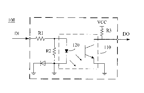
FIG. 1 is a schematic circuit diagram of a digital signal input circuit. It
can be learned from a
circuit 100 shown in FIG. 1 that a digital signal is inputted from a digital
input (Digital In, DI)
port, and is inputted into an isolating circuit 110 after voltage division by
means of a resistor
R1 and a resistor R2. A light emitting diode 120 in the isolating circuit
determines whether a
level of the digital signal is a high level or a low level. Finally, the level
of the digital signal is
converted, by using a pull-up resistor R3, into a level that can be supported
by a target ship.
The digital signal is outputted from a digital output (Digtal Out, DO) port,
and is inputted into
the target chip. In the circuit 100, the light emitting diode in the isolating
circuit determines
whether the level of the digital signal is a high level or a low level.
However, precision of
determining a level by a light emitting diode is relatively low, and a
conversion error easily
occurs when a level of a digital signal is converted.
SUMMARY
This application provides a digital signal input circuit, so as to increase
correctness of digital
signal level conversion.
A first aspect provides a digital signal input circuit, comprising an
isolating circuit and a
voltage determining circuit, wherein a first port of an input end of the
isolating circuit is
connected to an input end of the digital signal input circuit and configured
to receive a digital
1
CA 2980314 2019-01-14
84077273
signal, an output end of the isolating circuit is connected to an output end
of the digital signal
input circuit and configured to output a converted digital signal, and the
isolating circuit
outputs a first level when being open, or the isolating circuit outputs a
second level when
being closed; and an input end of the voltage determining circuit is connected
to the input end
of the digital signal input circuit and configured to receive the digital
signal, an output end of
the voltage determining circuit is connected to a second port of the input end
of the isolating
circuit, and the voltage determining circuit is configured to determine,
according to a level of
the digital signal, whether the isolating circuit is open or closed.
According to the digital signal input circuit, a voltage determining circuit
determines a level
of a digital signal, so as to avoid determining of a level of a digital signal
by means of a light
emitting diode in the prior art. In this way, correctness of digital signal
level conversion is
increased.
In a possible implementation, the voltage determining circuit includes a
voltage comparator, a
first input end of the voltage comparator is connected to the input end of the
digital signal, a
second input end of the voltage comparator is connected to a reference voltage
source, and an
output end of the voltage comparator is connected to a switching device, where
the voltage
comparator is configured to control an on/off state of the switching device
according to a
high-low relationship between the level of the digital signal and a level of
the reference
voltage source, and the switching device is configured to control the
isolating circuit to be
open or closed.
Optionally, the first input end of the voltage comparator is a non-inverting
input end, and the
second input end of the voltage comparator is an inverting input end.
In this solution, a voltage comparator in a voltage determining circuit
determines a level of a
digital signal, so as to avoid determining of a level of a digital signal by
means of a light
emitting diode in the prior art. In this way, correctness of digital signal
level conversion is
increased.
2
CA 2980314 2019-01-14
84077273
Further, generally, a digital signal level range supported by a voltage
comparator is larger than
a digital signal level range supported by a light emitting diode. That is,
compared with a
digital signal input circuit in the prior art, the digital signal input
circuit provided in this
solution can support a larger digital signal level conversion range.
Optionally, the first input end of the voltage comparator is a non-inverting
input end, and the
second input end of the voltage comparator is an inverting input end.
The foregoing switching device may be a bipolar transistor or a metal-oxide
semiconductor
(Metal Oxide Semiconductor, MOS) field-effect transistor.
Optionally, the voltage determining circuit includes a voltage comparator, a
first input end of
the voltage comparator is connected to the input end of the digital signal, a
second input end
of the voltage comparator is connected to a reference voltage source, and an
output end of the
voltage comparator is connected to a switching device by using a controller.
The voltage
comparator controls an on/off state of the switching device by using the
controller, and the
on/off state of the switching device can control the isolating circuit to be
open or closed.
In a possible implementation, the switching device is a bipolar transistor,
the output end of the
voltage comparator is connected to a base of the bipolar transistor, a
collector of the bipolar
2a
CA 2980314 2019-01-14
transistor is connected to the isolating circuit, and an emitter of the
bipolar transistor is grounded.
In a possible implementation, the voltage determining circuit further includes
a resistive voltage
division circuit, an input end of the resistive voltage division circuit is
connected to the input end of
the digital signal, and an output end of the resistive voltage division
circuit is connected to the
non-inverting input end of the voltage comparator, where the resistive voltage
division circuit is
configured to perform voltage division on the digital signal.
In this solution, a digital signal on which a resistive voltage division
circuit performs voltage
division is inputted into a voltage comparator. In this way, when a level
range supported by the
voltage comparator is fixed, the digital signal level range supported by the
voltage comparator is
expanded to some extent.
Further, a resistance value in the resistive voltage division circuit may be
further adjusted, so as to
adjust a digital signal level range supported by the digital signal input
circuit.
In a possible implementation, a collector of the isolating circuit includes a
photobipolar transistor,
an output end of the photobipolar transistor is connected to a power supply by
using a pull-up
resistor, the output end of the photobipolar transistor is connected to the
output end of the digital
signal, and the power supply is configured to provide a voltage to the pull-up
resistor to convert the
level of the digital signal into the first level or the second level.
In this solution, a level of a digital signal is adjusted by using a pull-up
resistor connected to an
output end of a photobipolar transistor, so as to adjust the level of the
digital signal to a level
supported by a target chip.
In a possible implementation, a collector of the isolating circuit includes a
photobipolar transistor,
an input end of the photobipolar transistor is connected to a power supply by
using a pull-up resistor,
the input end of the photobipolar transistor is connected to the output end of
the digital signal, and
the power supply is configured to provide a voltage to the pull-up resistor to
convert the level of the
digital signal into the first level or the second level.
In this solution, a level of a digital signal is adjusted by using a pull-up
resistor connected to an
input end of a photobipolar transistor, so as to adjust the level of the
digital signal to a level
supported by a target chip.
In a possible implementation, the digital signal input circuit further
includes a constant current
source circuit, and an emitter of the isolating circuit includes a light
emitting diode, where an input
end of the constant current source circuit is connected to the input end of
the digital signal, an
output end of the constant current source circuit is connected to the light
emitting diode of the
isolating circuit, and the constant current source circuit is configured to
provide a constant current
to the light emitting diode.
Optionally, the constant current source circuit is encapsulated into a
constant current source chip.
3
CA 2980314 2017-09-26
In this solution, a constant current source circuit provides a constant
current to a light emitting
diode, to ensure that the light emitting diode properly works.
In a possible implementation, the constant current source circuit includes a
first bipolar transistor, a
second bipolar transistor, and a resistor, a model of the first bipolar
transistor is the same as a model
of the second bipolar transistor, and the first bipolar transistor and branch
circuits in which the
resistor and the second bipolar transistor are located are connected in
parallel between the input end
and the output end of the constant current source circuit.
In this solution, a constant current is provided to a light emitting diode by
using a feature that BE
knot voltages of bipolar transistors with a same model are similar. This can
ensure that the light
emitting diode properly works.
BRIEF DESCRIPTION OF DRAWINGS
FIG 1 is a schematic circuit diagram of a digital signal input circuit in the
prior art;
FIG. 2 is a schematic circuit diagram of a digital signal input circuit
according to an embodiment of
the present invention;
FIG. 3 is a schematic circuit diagram of a principle of a voltage determining
circuit according to an
embodiment of the present invention;
FIG. 4 is a schematic circuit diagram of a principle of a voltage determining
circuit according to
another embodiment of the present invention; and
FIG. 5 is a schematic circuit diagram of a principle of a digital signal input
circuit according to
another embodiment of the present invention.
DESCRIPTION OF EMBODIMENTS
The following describes the technical solutions in the embodiments of the
present invention with
reference to the accompanying drawings in the embodiments of the present
invention. Apparently,
the described embodiments are some rather than all of the embodiments of the
present invention.
All other embodiments obtained by a person of ordinary skill in the art based
on the embodiments
of the present invention without creative efforts shall fall within the
protection scope of the present
invention.
FIG. 2 is a schematic circuit diagram of a digital signal input circuit
according to an embodiment of
the present invention. A circuit 200 shown in FIG. 2 includes a voltage
determining circuit 210 and
an isolating circuit 220.
Isolating circuit 220: A first port of an input end of the isolating circuit
is connected to an input end
4
CA 2980314 2017-09-26
of a digital signal, an output end of the isolating circuit is connected to an
output end of the digital
signal, and when the isolating circuit is open, the isolating circuit is
configured to output a first level,
or when the isolating circuit is disclosed, the isolating circuit is
configured to output a second level.
Voltage determining circuit 210: An input end of the voltage determining
circuit is connected to the
input end of the digital signal, an output end of the voltage determining
circuit is connected to a
second port of the input end of the isolating circuit, and the voltage
determining circuit is
configured to determine, according to a level of the digital signal, whether
the isolating circuit is
open or closed.
The foregoing digital signal may be a signal that carries a digital parameter.
The voltage determining circuit may determine, according to the level of the
digital signal, whether
the isolating circuit is open or closed, to control the level of the digital
signal that is outputted by
the isolating circuit. For example, when the voltage determining circuit
determines that the digital
signal is at a high level, the voltage determining circuit controls the
isolating circuit to be closed,
and the output end of the isolating circuit may adjust the high level of the
digital signal to a low
level in a range that can be supported by a chip. When the voltage determining
circuit determines
that the digital signal is at a low level, the voltage determining circuit
controls the isolating circuit
to be open, and the output end of the isolating circuit can adjust the low
level of the digital signal to
a high level in a range that can be supported by a chip.
The isolating circuit may convert the level of the digital signal into a first
level or a second level in
a range that can be supported by a target chip. The first level may be a high
level in the range that
can be supported by the target chip, and correspondingly, the second level may
be a low level in the
range that can be supported by the target chip. Alternatively, the first level
may be a low level in the
range that can be supported by the target chip, and correspondingly, the
second level may be a high
level in the range that can be supported by the target chip.
That the foregoing circuit converts the level of the digital signal into a
level that can be supported
by a chip further includes: converting a high level of the digital signal into
a low level that can be
supported by the chip, or converting a low level of the digital signal into a
high level that can be
supported by the chip.
The foregoing isolating circuit may be an optical coupling circuit, and the
optical coupling circuit is
generally a device that transmits an electrical signal by using light as a
medium. A light emitter (for
example, an infrared light emitting diode) and a light receiver (for example,
a photosensitive
semiconductor transistor) are generally encapsulated in a same pipe shell.
When an electrical signal
is inputted into an input end (that is, an emitter) at which the light emitter
is located, the light
emitter transmits a ray. An output end (that is, a collector) at which the
light receiver is located
receives the ray, and generates a photocurrent, which is outputted from the
output end of the
5
CA 2980314 2017-09-26
isolating circuit. In this way, "electric-photo-electric" conversion is
implemented, and electric
isolation is implemented at the input end of the isolating circuit and the
output end of the isolating
circuit.
Optionally, the foregoing isolating circuit may be an optical coupling
circuit. The first port of the
input end of the isolating circuit may be a port connected to a positive
electrode of a light emitting
diode in the optical coupling circuit, and the second port of the input end of
the isolating circuit may
be a port connected to a negative electrode of the light emitting diode.
Alternatively, the first port of
the input end of the isolating circuit may be a port connected to a negative
electrode of a light
emitting diode in the optical coupling circuit, and the second port of the
input end of the isolating
circuit may be a port connected to a positive electrode of the light emitting
diode. For the digital
signal input circuit shown in FIG. 1, that the output end of the voltage
determining circuit is
connected to the isolating circuit by using the second port of the input end
of the isolating circuit is
merely used as an example. The present invention sets no specific limitation
on a form of a
connection between the voltage determining circuit and the isolating circuit.
For ease of description below, the digital signal input circuit shown in FIG.
1 is referred to as a
branch circuit. The branch circuit may convert a digital signal at a high
level into a digital signal at
a low level, and the branch circuit may further adjust a level of a digital
signal to adapt to a digital
signal level range supported by a target chip.
Optionally, in an embodiment, the voltage determining circuit includes a
voltage comparator, a first
input end of the voltage comparator is connected to the input end of the
digital signal, a second
input end of the voltage comparator is connected to a reference voltage
source, and an output end of
the voltage comparator is connected to a switching device. The voltage
comparator is configured to
control a connectivity status of the switching device according to a high-low
relationship between
the level of the digital signal and a level of the reference voltage source,
and the switching device is
configured to control the isolating circuit to be open or closed.
The foregoing switching device may be a device such as a bipolar transistor or
a MOS transistor.
Optionally, the first input end of the voltage comparator is a non-inverting
input end, and the second
input end of the voltage comparator is an inverting input end. Specifically,
when the level of the
digital signal is higher than the level of the reference voltage source, the
voltage comparator outputs
a digital signal at a high level. When the level of the digital signal is
lower than the level of the
reference voltage source, the voltage comparator outputs a digital signal at a
low level.
Optionally, the first input end of the voltage comparator is an inverting
input end, and the second
input end of the voltage comparator is a non-inverting input end.
Specifically, when the level of the
digital signal is higher than the level of the reference voltage source, the
voltage comparator outputs
.. a digital signal at a low level. When the level of the digital signal is
lower than the level of the
6
CA 2980314 2017-09-26
reference voltage source, the voltage comparator outputs a digital signal at a
high level.
Optionally, the voltage determining circuit includes a voltage comparator, a
first input end of the
voltage comparator is connected to the input end of the digital signal, a
second input end of the
voltage comparator is connected to a reference voltage source, and an output
end of the voltage
comparator is connected to a switching device by using a controller. The
voltage comparator
controls an on/off state of the switching device by using the controller, and
the on/off state of the
switching device may be used to control the isolating circuit to be open or
closed.
The foregoing switching device may be a bipolar transistor or a MOS
transistor. The foregoing
controller may be a microcontroller unit (Microcontroller Unit, MC1.1), or the
foregoing controller
may be another device that can control, by using the switching device, the
isolating circuit to be
open or closed. This embodiment of the present invention sets no limitation on
a specific
implementation form of the controller.
Optionally, the output end of the voltage comparator is connected to a base of
the bipolar transistor,
a collector of the bipolar transistor is connected to the isolating circuit,
an emitter of the bipolar
transistor is grounded, and the voltage comparator controls, by using the
bipolar transistor, the
isolating circuit to be open or closed.
For example, FIG. 3 shows a schematic circuit diagram of a principle of a
voltage determining
circuit according to an embodiment of the present invention. It should be
understood that a circuit
300 shown in FIG. 3 may be at a location of 211 in FIG. 2. An input end of a
digital signal is
connected to a non-inverting input end of a voltage comparator 310, an
inverting input end of the
voltage comparator 310 is connected to a reference voltage source, and an
output end of the voltage
comparator is connected to a base of a bipolar transistor 320 by using a
resistor R. The resistor R
may be used to adjust a voltage that is outputted by the voltage comparator. A
collector of the
bipolar transistor is connected to an input end of an isolating circuit (which
is not shown in FIG. 3),
and an emitter of the bipolar transistor may be grounded.
When a level of a digital signal that is inputted by the input port of the
digital signal is higher than a
voltage of the reference voltage source, the voltage comparator outputs a
digital signal at a high
level, and the high level may be used as a voltage of the emitter of the
bipolar transistor. When a
voltage of the high level is greater than a breakover voltage of a PN knot of
the bipolar transistor,
the bipolar transistor is in a conductive state, that is, a branch circuit in
which the input end of the
isolating circuit that is connected to the bipolar transistor is in a
conductive state. That is, a
photodiode in the isolating circuit is conductive.
In the foregoing schematic circuit diagram, the voltage determining circuit is
only used to
implement a principle of voltage determining. In an implementation process,
various variations may
be made to the foregoing circuit diagram, and a new device may be added in the
foregoing circuit
7
CA 2980314 2017-09-26
diagram. The present invention sets no specific limitation on a connection
manner of the voltage
determining circuit.
In a process of implementing the foregoing voltage determining circuit, the
voltage determining
circuit may be implemented by using a dedicated chip of the voltage
determining circuit, or may be
implemented by using an operation amplifying circuit. The present invention
sets no specific
limitation on an implementation form of the voltage determining circuit.
Optionally, the voltage determining circuit further includes a resistive
voltage division circuit, an
input end of the resistive voltage division circuit is connected to the input
end or the digital signal,
and an output end of the resistive voltage division circuit is connected to
the non-inverting input
end of the voltage comparator, where the resistive voltage division circuit is
configured to perform
voltage division on the digital signal.
For example, FIG. 4 is a schematic circuit diagram of a principle of a voltage
determining circuit
according to another embodiment of the present invention. It should be
understood that a same
reference sign is used for a same device in the circuit diagram shown in FIG.
4 and the circuit
diagram shown in FIG. 3. For brevity, details are not described herein.
Based on the voltage determining circuit 300 shown in FIG. 3, a resistive
voltage division circuit
410 is added to a voltage determining circuit 400 shown in FIG. 4. It can be
learned from the
resistive voltage division circuit 410 shown in FIG. 4 that the resistive
voltage division circuit may
include a first resistor 420 and a second resistor 440. One end of the first
resistor is connected to an
input end of a digital signal, the first resistor and the second resistor are
serially connected, and an
output end of the resistive voltage division circuit is connected to a non-
inverting input end of the
voltage comparator 310. When the digital signal is inputted from an input end,
the first resistor and
the second resistor that are serially connected perform voltage division, and
the digital signal is
outputted from an output end 430 between the first resistor and the second
resistor.
Resistance values of the first resistor and the second resistor in the
resistive voltage division circuit
may be set according to a related performance parameter of a voltage
comparator. The present
invention sets no specific limitation thereto.
The foregoing resistive voltage division circuit is configured to perform
voltage division on a level
of a digital signal, to expand a digital signal level range. The present
invention sets no specific
limitation on a form of a voltage division circuit. There may be another
circuit that can be used for
voltage division or voltage stabilization.
When a resistance value of the first resistor 420 is RI, a resistance value of
the second resistor 440
is R2, a voltage of a reference voltage source of the voltage comparator is
Vref, and a maximum
voltage that can be supported by a target chip is Vmax= Therefore, a digital
signal voltage range that
can be supported by the voltage determining circuit may be Vref x (RI + R2)/R2
to Vmax X (R1 +
8
CA 2980314 2017-09-26
R2)/R2. When the level of the digital signal is lower than Vref, the voltage
comparator does not
work.
Optionally, a collector of the isolating circuit includes a photobipolar
transistor, an output end of the
photobipolar transistor is connected to a power supply by using a pull-up
resistor, the output end of
the photobipolar transistor is connected to the output end of the digital
signal, and the power supply
is configured to provide a voltage to the pull-up resistor to convert the
level of the digital signal into
the first level or the second level.
For example, when a level that is outputted by the isolating circuit is less
than a voltage range that
can be supported by the target chip, the pull-up resistor may be used to
provide a current component
to "pull high" the level of the digital signal, so as to meet a level that can
be supported by the target
chip.
Optionally, in an embodiment, the digital signal input circuit further
includes a constant current
source circuit, and an emitter of the isolating circuit includes a light
emitting diode. An input end of
the constant current source circuit is connected to the input end of the
digital signal, an output end
of the constant current source circuit is connected to the light emitting
diode of the isolating circuit,
and the constant current source circuit is configured to provide a constant
current to the light
emitting diode.
The foregoing constant current source circuit may be implemented by using a
transistor, may be
implemented by using a field effect, or may be implemented by using a shunt
regulator. The present
invention sets no specific limitation on an implementation form of the
constant current source
circuit.
Optionally, the constant current source circuit includes two bipolar
transistors with a same model
and a resistor, the two bipolar transistors include a first bipolar transistor
and a second bipolar
transistor, and the first bipolar transistor and branch circuits in which the
resistor and the second
bipolar transistor are located are connected in parallel between the input end
and the output end of
the constant current source circuit.
FIG. 5 shows a schematic circuit diagram of a principle of a digital signal
input circuit according to
another embodiment of the present invention. It should be understood that a
same reference sign is
used for a device in the circuit shown in FIG. 5 and a device in the circuit
diagram shown in FIG. 2.
For brevity, details are not described herein. A circuit 500 shown in FIG. 5
includes a constant
current source circuit 510. It can be learned from FIG. 5 that a constant
current source circuit 510
includes two bipolar transistors with a same model: a bipolar transistor 511 a
bipolar transistor 512.
The constant current source circuit may provide a relatively constant current
to a photodiode in the
isolating circuit 220 by using a resistor R5 and a relatively stable voltage
(a BE knot voltage)
between a base (also referred to as a B electrode) and an emitter (also
referred to as an E electrode)
9
CA 2980314 2017-09-26
of the bipolar transistor 511 and the bipolar transistor 512.
In the schematic circuit diagram of the constant current source circuit 510
shown in FIG. 5, the
devices in the constant current source circuit may be modified, or another
device may be added to
improve performance of the constant current source circuit. The present
invention sets no specific
limitation on a connection form of the constant current source circuit.
It should be understood that sequence numbers of the foregoing processes do
not mean execution
sequences in various embodiments of the present invention. The execution
sequences of the
processes should be determined according to functions and internal logic of
the processes, and
should not be construed as any limitation on the implementation processes of
the embodiments of
the present invention.
A person of ordinary skill in the art may be aware that, the units and
algorithm steps in the
examples described with reference to the embodiments disclosed in this
specification may be
implemented by electronic hardware or a combination of computer software and
electronic
hardware. Whether the functions are performed by hardware or software depends
on particular
.. applications and design constraint conditions of the technical solutions. A
person skilled in the art
may use different methods to implement the described functions for each
particular application, but
it should not be considered that the implementation goes beyond the scope of
the present invention.
The foregoing descriptions are merely specific implementations of the present
invention, but are not
intended to limit the protection scope of the present invention. Any variation
or replacement readily
figured out by a person skilled in the art within the technical scope
disclosed in the present
invention shall fall within the protection scope of the present invention.
Therefore, the protection
scope of the present invention shall be subject to the protection scope of the
claims.
CA 2980314 2017-09-26