Note: Descriptions are shown in the official language in which they were submitted.
CA 02981695 2017-10-03
WO 2016/159788
PCT/NZ2016/050055
1
INDUCTIVE POWER TRANSMITTER
FIELD
The invention generally relates to an inductive power transmitter for
lo inductive power transfer (IPT) and in particular foreign object
detection.
BACKGROUND
IPT is a well-known area of established technology used in many
applications including wireless charging of portable electric devices. A
charging mat is one way of providing a charging surface for a portable
device and has an interface surface incorporating a power transmitter with
one or more transmitting coils that generate a time-varying magnetic field.
The magnetic field induces an alternating current in a suitable receiving
coil of a power receiver that can then be used to charge a battery, or
power a device or other load.
It is particularly important that IPT systems for wireless power transmitter
transfers power to power receiver only and not to so-called 'foreign
objects'. Foreign objects are defined as any object that is positioned on a
charging mat but are not part of a receiver device. Typical examples of
such foreign objects are metallic elements such as coins, keys, paperclips,
etc. For example, if a metal object is close to the active IPT field it could
be heated due to eddy currents being developed from the oscillating
magnetic field. In order to prevent the temperature of such parasitic metal
from rising to unacceptable levels, the power transmitter should be able to
discriminate between power receivers and foreign objects and reduce the
power being transferred or abort operation altogether.
CA 02981695 2017-10-03
WO 2016/159788
PCT/NZ2016/050055
2
One method in the art for detecting foreign objects is known as a power
loss method. In this method, the received power is indicative of the total
amount of power dissipated within a power receiver contained in a
handheld device due to the magnetic field produced by the power
transmitter. The received power equals the power that is available from
the output of the power receiver plus any power that is lost in producing
that output power. The power receiver communicates its received power
back to the power transmitter so that the power transmitter is able to
determine whether the power loss is within acceptable set limits, and if
not, the power transmitter determines anomalous behaviour indicative of
the presence of a foreign object. However, power loss accounting does
not in itself provide actual detection of a foreign object, only the
occurrence of non-expected behaviour. Further, the transmitter and
receiver must be preconfigured to communicate with one another thereby
limiting the versatility of the devices and the accuracy varies widely
depending on the distance between the transmitter and the receiver.
Another method in the art is described in international patent publication
number W02014/095722 where foreign objects are detected by separate
excitation and detection coils within the transmitter. The method describes
detecting changes in the output voltage in the detection coil, or changes in
the inductance of the detection coil to determine the presence of a foreign
object. However, this method requires complex calibration to determine
the base inductance characteristics. This method is also unable to
distinguish between metal objects ferrous or magnetic objects and
therefore does not provide a means to discriminate between foreign
objects and friendly objects such as a receiver device. Any undesirable
effects of operation of the primary IPT field on the detection are also not
considered or characterised, this method is therefore unreliable.
CA 02981695 2017-10-03
WO 2016/159788
PCT/NZ2016/050055
3
Another method in the art is described in US patent application
20130176023 where foreign objects are detected by actively monitoring
the quality factor or Q value of a receiver coil by measuring changes in
voltage across as inductor. Foreign objects are detected by actively
generating a resonating voltage in a receiver or detection coil and then
detecting the Q value changes via the transmitter coil. However, this
method incorporates losses from both the transmitter and receiver coil and
therefore lends to inaccuracies as losses caused by the receiver are
indistinguishable from losses caused by other components in the system
such as foreign objects. Further, separate circuits on the receiver and
transmitter are required to provide this functionality, lending toward
increased manufacturing cost and physical size requirements.
The present invention may provide an improved inductive power
transmitter or may at least provide the public with a useful choice.
SUMMARY
According to one example embodiment there is provided an inductive
power transmitter comprising
at least one power transmitting coil configured to generate an
inductive power transfer (IPT) field, and
an object detection (OD) system configured to detect the presence
of an object based on a change in energy decay or change in resonant
frequency of a resonant circuit integrated with or coupled to the
transmitting coil.
It is acknowledged that the terms "comprise", "comprises" and
"comprising" may, under varying jurisdictions, be attributed with either an
exclusive or an inclusive meaning. For the purpose of this specification,
and unless otherwise noted, these terms are intended to have an inclusive
CA 02981695 2017-10-03
WO 2016/159788
PCT/NZ2016/050055
4
meaning ¨ i.e., they will be taken to mean an inclusion of the listed
components which the use directly references, and possibly also of other
non-specified components or elements.
Reference to any document in this specification does not constitute an
io admission that it is prior art, validly combinable with other documents
or
that it forms part of the common general knowledge.
BRIEF DESCRIPTION OF THE DRAWINGS
The accompanying drawings which are incorporated in and constitute part
of the specification, illustrate embodiments of the invention and, together
with the general description of the invention given above, and the detailed
description of embodiments given below, serve to explain the principles of
the invention.
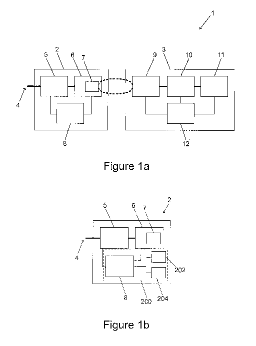
Figure la is a schematic of an inductive power transfer system.
Figure lb is a block diagram of an object detection system.
Figure 2 is a schematic diagram of a resonant tank in an inductive
power transfer system.
Figure 3 is a graph of energy decay in the resonant tank of Figure 2.
Figure 4(a) is circuit diagram of a resonant tank circuit.
Figure 4(b) is a graph of energy decay in the circuit of Figure 4(a) as a
function of time.
Figure 5(a) is circuit diagram of a resonant tank circuit and a proximate
inductive power receiver.
CA 02981695 2017-10-03
WO 2016/159788
PCT/NZ2016/050055
5 Figure
5(b) is a graph of energy decay in the circuit of Figure 4(a) as a
function of time.
Figure 6(a) is circuit diagram of a resonant tank circuit and a model of a
proximate foreign object.
Figure 6(b) is a graph of the corresponding energy in the resonant tank
1.0 circuit as a function of time.
Figure 7 is
circuit diagram of one example of an inductive power
transmitter circuit comprising three inductive power
transmission coils.
Figure 8 is
circuit diagram of another example of an inductive power
transmitter circuit comprising three resonator tank circuits
located separate but proximate to three inductive power
transmission coils.
Figure 9a is
circuit diagram of another example of an inductive power
transmitter circuit.
Figure 9b is a graph of
voltages during operation of a resonator circuit
that is inductively coupled to a power transmission coil such
as the example shown in Figure 9(a).
Figure 10 is a
schematic of an example circuit where multiple different
frequencies may be generated.
Figure 11 is circuit
diagram of energy inductively coupled to the coil
Li 0 of the resonator circuit by another coil.
Figure 12 is
circuit diagram of energy coupled to the resonator by a
switch M2 controlling coupling of energy from a DC source.
CA 02981695 2017-10-03
WO 2016/159788
PCT/NZ2016/050055
6
Figure 13 is a graph of
frequency response of a tank circuit as shown in
Figure 1.
Figure 14a is a top view of a source coil positioned within a concentrically
arranged resonator coil.
Figure 14b shows a top view of an alternative arrangement having the
1.0
resonator coil positioned within a concentrically arranged
source coil.
Figure 14c shows a top view of a further alternative arrangement with a
source coil positioned to overlap with two resonator coils.
Figure 14d shows a top view of a further alternative arrangement where
an inner centric source coil is positioned within two outer
concentric resonator coils in a cascaded configuration.
DETAILED DESCRIPTION
An inductive power transfer (IPT) system 1 is shown generally in Figure
la. The IPT system typically comprises an inductive power transmitter 2
and an inductive power receiver 3. The inductive power transmitter 2 is
connected to an appropriate power supply 4 such as mains power or a
battery. The inductive power transmitter 2 may include transmitter circuitry
having one or more of a converter 5, e.g., an AC-DC converter (depending
on the type of power supply used) and an inverter 6, e.g., connected to the
converter 5 (if present). The inverter 6 supplies a transmitting coil or coils
7 with an AC signal so that the transmitting coil or coils 7 generate an
alternating magnetic field. In some configurations, the transmitting coil(s)
7 may also be considered to be separate from the inverter 5. The
transmitting coil or coils 7 may be connected to capacitors (not shown)
either in parallel or series to create a resonant circuit.
CA 02981695 2017-10-03
WO 2016/159788
PCT/NZ2016/050055
7
A controller 8 may be connected to each part of the IPT transmitter 2. The
controller 8 may be adapted to receive inputs from each part of the IPT
transmitter 2 and produce outputs that control the operation of each part.
The controller 8 may be implemented as a single unit or separate units,
lo configured to control various aspects of the IPT transmitter 2
depending
on its capabilities, including for example: foreign object detection, power
flow, tuning, selectively energising transmitting coils, inductive power
receiver detection and/or communications. The controller 8 may have one
or more units/components, and may be a controller such as a
microcontroller, PID, FPGA, CPLD, ASIC, etc. Further, it may be possible
to integrate significant parts of the entire wireless receiver circuit onto a
single integrated circuit.
The inductive power receiver 3 includes a receiving coil or coils 9
connected to receiver circuitry which may include power conditioning
circuitry 10 that in turn supplies power to a load 11. When the coils of the
IPT transmitter 2 and the inductive power receiver 3 are suitably coupled,
the alternating magnetic field generated by the transmitting coil or coils 7
induces an alternating current in the receiving coil or coils 9. The power
conditioning circuitry 10 is configured to convert the induced current into a
form that is appropriate for the load 11, and may include for example a
power rectifier, a power regulation circuit, or a combination of both. The
receiving coil or coils 9 may be connected to capacitors (not shown) either
in parallel or series to create a resonant circuit. In some inductive power
receivers, the receiver may include a controller 12 which may control
tuning of the receiving coil or coils 9, operation of the power conditioning
circuitry 10 and/or communications.
The term "coil" may include an electrically conductive structure where an
electrical current generates a magnetic field. For example inductive "coils"
CA 02981695 2017-10-03
WO 2016/159788
PCT/NZ2016/050055
8
may be electrically conductive wire in three dimensional shapes or two
dimensional planar shapes, electrically conductive material fabricated
using printed circuit board (PCB) techniques into three dimensional
shapes over plural PCB 'layers', and other coil-like shapes. The use of the
term "coil" in either singular or plural is not meant to be restrictive in
this
sense. Other configurations may be used depending on the application.
It may be desirable in certain applications for the IPT transmitter to
selectively provide power to associated receiver devices (e.g., mobile
phones, remote controls, etc.) and not to foreign objects (FO) (e.g.,
paperclips, coins, etc.). To this end, the IPT transmitter may include an
Object Detection (OD) system. The OD system may either deactivate
coils in response to non-receiver devices or only activate coils in the sole
presence of receiver devices. In situations where there is a plurality of
transmitting coils, such as an array of coils (e.g., on a charging mat), the
OD system may only de/activate, a subset of coil/s according to the
location of the receiver / non-receiver device respectively.
In general terms this embodiment may include charging a coil with an
initial known energy, removing the energisation and then comparing the
decay performance against known characteristics for foreign objects or
non-receiver devices, receiver devices and/or no devices.
An example transmitter 2 is shown in Figure 1 b. The inverter 6 supplies
power to the transmitting coil 7 to generate an IPT field. An OD circuit 200
includes an excitation coil or coils 202 to generate a OD field and/or an
initial detection energy and a detection circuit 204 used to sense the
presence and/or location of objects on or adjacent to the transmitter 2.
The controller 8 of the transmitter 2 may either directly or via a separate
control circuit be configured to determine the excitation to be provided to
CA 02981695 2017-10-03
WO 2016/159788
PCT/NZ2016/050055
9
the excitation coil 202 and process the output signal from the OD circuit
204.
This may involve an array of coils, and/or or a plurality of OD circuits (and
either using the IPT frequency or modulating an excitation signal onto the
lo IPT field) depending on the requirements of the application.
The OD field may be generated by the transmitting coil 7 or may be a
separate coil, coupled or otherwise. It may be operated sequentially with
the IPT field or simultaneously. If it is operated simultaneously it may be
desirable to operate the OD field at a different frequency. The advantage
of operating at a different frequency to the IPT frequency is that receiver
devices will effectively appear invisible (as they are tuned to only receive
power at the resonant IPT frequency). This may allow the system to be
designed to be more sensitive to the introduction of a FO even in the
overlapping presence of a receiver object.
For example, the OD field may operate a 5-50kHZ and the IPT field may
operate at 50kHz-500kHz. The OD field and can be tuned to a frequency
higher or lower than the IPT field. To ensure the best operation
performance in the presence of a receiver object, the OD field may be
tuned to a frequency at least five times away from it. For example, for an
IPT frequency of 100kHz the OD frequency can be tuned to 20kHz or less,
or for an IPT frequency of 200kHz the OD frequency can be tuned to at
least 1Mhz. Further it may be desirable that the IPT frequency is not a
harmonic of the OD frequency or vice versa, to avoid and harmonic
resonances in receiver devices (and therefore resulting receiver losses
from the OD field). For example, if the IPT transmitter is configured to
operate at 100 kHz the OD coil may be configured to operate at 10.5 kHz
or some offset.
CA 02981695 2017-10-03
WO 2016/159788
PCT/NZ2016/050055
5 The IPT transmitter 2 comprises a capacitor selectively coupled to the
transmitting coil(s) 7 for form a high Q resonant tank. The 0-value is an
index indicating the degree of resonance of a resonant circuit at a
resonant frequency. A high Q resonant tank circuit sustains an oscillation
longer than lower Q circuit. Since it is the envelope of the oscillations that
10 determines the rate of decay, more oscillation (higher Q) means easier
and more accurate detection. Additionally, the measured decay rate or
power loss is influenced by both the ESR of the coil (Q) and losses due to
F0s, higher Q (lower ESR) therefore means a smaller and more accurate
FO loss can be measured. For example, it is more difficult to accurately
determine an additional FO loss of 250mW on top of a 2W coil ESR loss
than the same FO loss on top of a 250mW coil ESR loss.
Figure 2 shows of a resonant circuit tank circuit 20 comprising a capacitor
C3 and inductor coil Li. This may be energised by inverter 6 at a desired
frequency and magnitude to generate a desired initial energy level. The
decay of the energy level after the inverter 6 is disconnected is then
measured. If energy is wirelessly coupled to the resonant tank, the
frequency used affects how much energy couples into the resonant tank
as more energy is coupled if frequency is similar to the resonant
frequency.
A larger initial energy causes a larger current to flow which induces a
larger power loss in the FO. Similarly, a distant FO will generate a smaller
power loss and be increasingly undetectable the further it is from the
transmitter. Therefore the level of initial energy provided to the resonant
circuit could be selected on whether a FO is within effective range of the
IPT transmitter, or on a minimum detection distance.
Further, as a receiver gets closer its induced loss becomes increasingly
larger (even though the FO frequency is not tuned to the Rx resonant
CA 02981695 2017-10-03
WO 2016/159788
PCT/NZ2016/050055
11
frequency). At some point these two losses will cross over and then it will
be impossible to tell them apart. Therefore it is important to energize the
resonant coil at the appropriate amount of energy to capture the FO
induced loss but not receiver induced loss.
Figure 3 shows a graph of energy decay in the resonant tank of Figure 2.
The tank is energised before t=0 and at t=0 energisation is stopped to
produce a known energy trapped in the tank of E=1/2*C*VA2. The voltage
across the capacitor Cl is measured after a time period that allows for
measureable energy decay to occur. In some embodiments, the period is
0.5 milliseconds, however the particular time period should be selected to
account for a portion of according to generally expected decay times. The
difference in energy before and after the decay time is power loss due to
natural loss due to coil and capacitor resistance and any loss created by
foreign objects in the inductive field. Knowledge of the energy loss for an
unobstructed field, and a field whereby an inductive power receiver is
present, can then be compared to any new field measurements to enable
a determination of whether a foreign object is present in the field.
Measurement of the capacitor voltage is ideally performed by envelope
detection or similar methods for peaks of the waveform, such as
measurement of the peak voltage of each cycle. The energy can
=
E 12
determined from the measured voltage using 2-C1
, where C is known
beforehand. The capacitance value is not affected by the presence of
ferrites or reflected impedances. The peak terminal voltage is therefore a
direct measurement of the energy in the tank.
Figures 4 to 6 show example energy decay data for three scenarios. In
particular, Figure 4(a) shows a resonant tank circuit 20 configured to
resonate at 10 kHz and Figure 4(b) shows graph of corresponding energy
CA 02981695 2017-10-03
WO 2016/159788
PCT/NZ2016/050055
12
in the circuit as a function of time. The rate of energy decay is indicative
of
no foreign objects being present in the field.
Figure 5(a) shows a resonant tank circuit 20 with an IPT receiver circuit 21
having receiver coil L2 positioned in proximity to the transmitter coil L1.
lo Figure
5(b) shows graph of the corresponding energy in the resonant tank
circuit as a function of time and in particular shows a largely similar rate
of
energy decay compared to the unobstructed field of Figure 4.
Figure 6(a) shows a resonant tank circuit 20 with a circuit model of a
metallic foreign object 22 having equivalent inductance L9 and resistance
R4 in the proximity of the transmitter coil. Figure 6(b) shows a graph of the
corresponding energy in the resonant tank circuit as a function of time and
in particular shows a rapid rate of decay compared to the decay rates of
Figures 4(b) and 5(b) due to the increased losses.
The rate of decay, or similarly, the energy remaining in the resonant tank
after a time period is indicative of the nature of objects in proximity to the
transmitter coil. The nature of objects in proximity to the transmitter coil
is
therefore able to be determined by comparison of the energy remaining in
the resonant tank after a time period is with one or more energy thresholds
or energy ranges.
Foreign object detection may therefore possible without the presence of
an inductive power receiver present in the generated field. The accuracy
of detection may be improved by mitigating or avoiding energy losses due
to the presence of a receiver that a detection system in the transmitter
would otherwise be exposed to. A further advantage may be that
communication between the power transmitter and power receiver is not
required.
CA 02981695 2017-10-03
WO 2016/159788
PCT/NZ2016/050055
13
In some embodiments, the transmitter comprises a coil configured for
inductive power transmission and also for generation of an OD field. In
alternative embodiments, the transmitter comprises a coil for inductive
power transmission and a separate coil for generation of the OD field.
lo Figure 7 shows one example of an inductive power transmitter circuit
comprising three inductive power transmission coils L7, L8 and L9 each
having a resonant tank circuit. The values of capacitors C8, C10 and C12
of 25.3 uF and the values of inductors L7, L8 and L9 of 10 uF configure
each resonant tank tuned to a frequency of 10 kHz. Capacitors C7, C9
and C11 are configured in to AC couple switches M8, M10 and M12. The
inductor of the resonant tank incorporates a coil from the power
transmitter. The IPT field is temporarily ceased while the OD field is
generated by disconnecting switches M8, M10 and M12 and connecting
switches M9, M11 and M13.
Where the IPT field is temporarily disabled while an FOD field is
generated, the off time of the transmitter should be such that normal
operation of the power receiver is not substantially affected. For example,
avoidance of output voltage ripple or reinitializing of communications is
preferable.
In other embodiments, the OD field can be superimposed upon the IPT
field, both of which are generated by the power transmitter coil. Power
transmission can advantageously be maintained constantly while the OD
field is generated periodically. For example, Figure 8 shows an inductive
power transmitter circuit comprising three resonator tank circuits located
separate but proximate to three inductive power transmission coils.
Operation of the inductive power transmission coils L1, L3, L5 is
temporarily stopped while each resonator tank circuit is operated when
desired for object detection. Each of the power transmission inductor coils
CA 02981695 2017-10-03
WO 2016/159788
PCT/NZ2016/050055
14
L1, L3 and L5 are driven by the inverter at 100 kHz. Each resonator tank
comprising the combination of L2 C2, L4 C4 and L8 C8 is configured to
resonate at 10 kHz so as to not have impact on the IPT field during
operation of the OD field. When switches M3, M4 and M5 are opened, the
residual energy in coils L2, L4 and L6 allow the circuit to resonate and act
lo as the OD coil.
Figure 9(a) shows another example circuit where the IPT coil forms a part
of the resonant tank by connection of a series capacitor C1 to the IPT coil
L1. In this circuit, operation of the IPT field and OD field are able to occur
simultaneously and the IPT field is superimposed with the OD field. Figure
9(b) shows a graph of voltages during operation of such resonator circuit
shown in Figure 9(a). During time period 30, an IPT coil has a
transmission coil current driven by an inverter (M1 &M2) at a frequency of
100 kHz as shown. Capacitor C1 and switch M3 form an AC switch for
amplitude control of the field in each coil. When this is used in combination
with amplitude control over an array, the overall field direction in 3D may
be controlled.
M4 is shorted for a period to control the peak value of the FOD decay
envelope (the peak value is also determined by the value of R). Capacitor
C1 has a value selected to resonate with L1 at 10 kHz. Switch M4
provides a compatible energy source to allow L1 and C1 to resonate for a
short period.
At time 31, switch M4 is turned on for a short pulse (e.g. 50 us), this
introduces a perturbation and causes the inverter resonant circuit to
oscillate at its natural resonant frequency (given by the combination of L1
and C1). During time period 32, the OD field is superimposed upon the
IPT field such that they operate simultaneously. The OD field is shown
here to be of a lower frequency than the IPT field. At time point 33 the
CA 02981695 2017-10-03
WO 2016/159788
PCT/NZ2016/050055
5 energy
of the OD field has died away at a rate dependent upon the nature
of objects within the field. During time period 34, normal operation of the
inductive power transmission field continues. The current in a receiver
device within the OD field is not affected because it is not tuned to the OD
frequency. The switching voltage provided to switch M4 is shown to
lo connect
for a brief period at time 31 to thereby energise the resonator
circuit.
In some embodiments, a source coil is configured to inductively energize a
coil in a resonant tank circuit and that tank coil is responsible for
15
generating large IPT field required to transfer sufficient power. This
configuration is most suitable for low coupling (low k) applications such as
large air gaps). The OD field is generated directly on the source coil and
not coupled to it. Therefore in this case the source coil generates the OD
field, the resonator coil generates the IPT field which is energized from the
source coil. In other embodiments where there is no separate resonator
coil and there only source coils, then both OD field and IPT field are
generated on the source coils.
Figures 14(a) ¨ (d) show 3D flat arrangements for the source coil and
resonator coils configured for inductive coupling. For example, Figure
14(a) shows a top view of a source coil 40 positioned within a
concentrically arranged resonator coil 41. An inverter is configured to
supply power to the source coil 40. Figure 14(b) shows a top view of an
alternative arrangement having the resonator coil 41 positioned within a
concentrically arranged source coil 40. Figure 14(c) shows a top view of a
further alternative arrangement with a source coil 40 positioned to overlap
with two resonator coils 41. This arrangement may advantageously allow a
single source coil to drive multiple resonator coils. Figure 14(d) shows a
top view of a further alternative arrangement where an inner centric source
CA 02981695 2017-10-03
WO 2016/159788
PCT/NZ2016/050055
16
coil 40 is positioned within two outer concentric resonator coils 41, 42 in a
cascaded configuration.
In one exemplary embodiment, a resonator coil is loosely coupled to the
source coil (k around 0.2). A resonator circuit is tuned to a frequency
slightly lower than the operating frequency of the transmitter, for example
the transmitter is tuned to operate at 110kHz and the resonator is tuned to
100kHz). At 110kHz, the resonator appears like a inductor with a very
small inductance. Therefore with a small current flowing in the source coil,
a much larger current flows in the resonator coil. This means that the
resonator coil provides most of the VA required to transfer power
The coupling distance between the source coil and resonator coil K is not
particularly critical and is chosen in conjunction with how much the
resonator coil is compensated by the capacitor. For example, the coupling
factor K could be 0.2.
This arrangement presents further advantageous since only a small VA is
in the source coil, it can have a low natural Q without affecting the
coupling efficiency too much. A PCB track can be used to implement the
source coil thereby lowering manufacturing cost. The switches can be
rated at much lower rating because they only need to switch much smaller
VAs. The switching losses and conduction losses are lower. The reflected
real load onto the source coil can be detected more easily since its VA is
much smaller. The resonator circuit only consists of passive components
thereby allowing easy adjustment of the increase the natural Q of the
resonator coil. Further, when the receiver is close to the transmitter and
the coupling condition is good, the likely presence of a ferrite will increase
the inductance of coils which automatically reduces the total VA produced.
CA 02981695 2017-10-03
WO 2016/159788
PCT/NZ2016/050055
17
As mentioned above the resonant frequency of the resonant tank circuit 20
may be tuned to a frequency having significant separation from the
frequency used for IPT to a receiver coil depending on the application
requirements. Separation also potentially increases the sensitivity of
physically small metallic objects nearby the transmitter due to the
possibility of resonance being established in the object.
For example, the IPT frequency may be tuned to have an operating
frequency within the range of about 110 kHz to about 205 kHz. Further,
the resonant tank is tuned to have a resonant frequency is as high as in
the MHz region, for example about 1 MHz, or in the low kHz region, such
as about 5 kHz.
In some embodiments, the OD field is configured so that a range of OD
field frequencies are used, using so-called frequency "hopping" or
"sweeping". Several
different frequencies may be used about the
exemplary levels already described at which measurements for object
detection are made. For example, OD field frequencies higher than the
IPT field frequency measurements are taken at about 800 kHz, about 1
MHz and about 1.2 MHz, and for OD field frequencies lower than the IPT
field frequency measurements may be taken at each of about 1 kHz, about
5 kHz and about 10 kHz.
Frequency hopping advantageously provides the ability to increase
discrimination between foreign and friendly objects. For example, metal or
ferrite may provide similar response to the OD field at a particular OD field
frequency due to the selected OD field frequency being a harmonic of the
IPT field frequency. However, such materials will provide a different
response at different OD field frequencies whilst the response of non-
resonant objects is substantially independent of frequency. Therefore the
CA 02981695 2017-10-03
WO 2016/159788
PCT/NZ2016/050055
18
circuit is configurable to generate OD fields at various frequencies to
enable detection and distinguishing of various materials within an OD field.
OD fields of different frequencies are created by altering the capacitive
value of Cl in the resonant tank, shown as 2.53 microfarads, with a higher
and/or lower capacitive value. Frequency hopping or sweeping is achieved
by actively switching capacitive values in and out of the resonant tank by
the use of semiconductor switching devices. In some embodiments, the
controller 8 is configured to control operation of the switching devices and
energise the resonant tank to thereby control generation of a set of OD
fields at a range of frequencies.
Figure 10 shows a schematic of an example circuit where multiple different
frequencies may be generated to thereby provide, for example, IPT fields
and OD fields, or OD fields of varying frequencies. In particular, Figure 10
shows the resonant tank circuits 23 having a pair of capacitors able to be
connected in parallel by switches. By controlling operation of the switches
in the circuit, capacitors can be connected in parallel, or operated
individually thereby changing the tuned frequency according to a
relationship of f = (LC)-(:).5. For example, connection of switch M4 forms a
circuit having an operation frequency of 100 kHz determined by the C2
capacitor value of 25.3 nF. Connection of switches M4 and M5 form a
circuit having an operation frequency of 10 kHz determined by the C3
capacitor value of 2.52 uF. L2 can therefore be configured to resonate to
produce an IPT field when configured to operate at one frequency, such
as 100 kHz, and be further configured to operate at another frequency to
generate a FO field, such as 10 kHz.
The IPT coils can be arranged in a rectangular array structure and may be
linear (2D), overlapping or three dimensionally arranged. The coil and
CA 02981695 2017-10-03
WO 2016/159788
PCT/NZ2016/050055
19
array can also be arranged to have a different geometrical or arbitrary
shape.
Figure 11 and Figure 12 show example embodiments configured to
energise the resonator to thereby generate an OD field from a coil. In
lo particular, Figure 11 shows energy is coupled to the coil L1 of the
resonator circuit inductively by another coil L11. Coil L11 is selectively
energised by a solid state switch M1, for example, as an IRF1503 FET as
shown. Figure 12 shows energy coupled to the resonator by a switch M2
controlling coupling of energy from a DC source V2.
Absolute measurements are able to be taken from the OD field as it is
decoupled from the IPT field. However, a FO will not be detected but will
merely be part of the ambient environment if a FO is already present on
the transmitter 'pad' at start-up. Therefore, in some embodiments, the
controller 8 is configured to precalibrate the system. For example, a
calibration token which is either physical, for example a metal disc, or
digital, for example a calibration factor of known properties is used to
calibrate the transmitter prior to use. By locating the token in particular
locations and adjusting the algorithm output until the location and object
type are correctly determined. In other embodiments, relative phase and
amplitude measurements between the primary, excitation and detection
coils are compared to relative expected values to determine whether there
is anything unusual in the start-up environment. In some embodiments an
alert is generated to manually check the environment or in other
embodiments the output is used to adjust the algorithm.
In some embodiments, changes in the natural resonant frequency of the
resonant tank circuit are detectable when any FOs are located within the
object detection field. The reflected impedance from FOs and ferrite
affects the resonant frequency of the resonant tank circuit. Therefore
CA 02981695 2017-10-03
WO 2016/159788
PCT/NZ2016/050055
5
monitoring for changes in the resonant frequency of the tank circuit is
indicative of a FO being present in the detection field. FOs such as metals
reflect a capacitive and a resistive load back to the primary coil which is
able to be detected by looking at the phase and amplitude of the induced
voltage and/or current. One method of measuring the frequency is to
lo sample
the OD current in the source coil in a micro-controller. Changes in
the resonant frequency are indicative of a change in the reflected
impedance or change in inductance is, and based on that the nature of
FOs can be predicted.
15
Measuring the resonant frequency may be simpler and requires minimal
circuitry. However frequency measurement is most suitable for high k
situations. In low k conditions the reflected impedance or effects of ferrites
become too small to detect, and therefore relying on measuring frequency
changes becomes unreliable under low k conditions. In addition the
20 presence
of both ferrite and metal together could cause a small overall
change in resonant frequency, therefore making the detection method
unreliable in certain cases. These shortcomings are overcome by the use
of energy decay to indicate the presence of FOs as there is no
dependency on k or placement of the objects.
Figure 13 shows an example of a graph of frequency response of a tank
circuit as shown in Figure 1. In some embodiments, the controller 8 is
configured to determine the resonance frequency of the resonant tank
circuit, for example, by measuring the time period between one or more
half wavelengths of the oscillating voltage such as zero crossings. In
Figure 6, the introduction of a reflected capacitive load has the effect of
increasing the resonance frequency. Conversely, the presence of ferrites
such as from a nearby IPT receiver has the effect of reducing the
resonance frequency.
CA 02981695 2017-10-03
WO 2016/159788
PCT/NZ2016/050055
21
Therefore the use of a high Q resonant tank in conjunction with the coil of
an IPT transmitter alone is able to be used to accurately measure power
loss cause by FOs, and distinguish FOs from an IPT receiver. By
measuring the rate of energy decrease in the tank, losses can be
measured and attributed to FOs and IPT receivers. Further, losses due to
lo an IPT receiver in proximity to the detection field are able to be
avoided if
the tank is tuned to a frequency very different from the IPT frequency. In
such embodiments, measured losses are purely due to coil natural losses,
which can be simply compensated for, and losses caused by FOs.
Further, when both a FO and a receiver are present together and they are
both far away. Existing FOD methods cannot detect a FO because a low k
means the reflected impedance is too small to detect. The proposed
method only looks at power losses and does not depend on k. Therefore
even if an FO is far away, as long as it induces power loss to the OD field,
it can be detected as an increase in energy decay rate.
While the present invention has been illustrated by the description of the
embodiments thereof, and while the embodiments have been described in
detail, it is not the intention of the Applicant to restrict or in any way
limit
the scope of the appended claims to such detail. Additional advantages
and modifications will readily appear to those skilled in the art. Therefore,
the invention in its broader aspects is not limited to the specific details,
representative apparatus and method, and illustrative examples shown
and described. Accordingly, departures may be made from such details
without departure from the spirit or scope of the Applicant's general
inventive concept.