Note: Descriptions are shown in the official language in which they were submitted.
CA 02982449 2017-10-11
WO 2016/168249 PCT/US2016/027215
MAGNETIC COIL POWER METHODS AND APPARATUS
TECHNICAL FIELD
[0001] This disclosure relates generally to power components for magnetic
coils and,
more particularly, to power components for driving one or more gradient coils
in a magnetic
resonance imaging system.
BACKGROUND
[0002] Magnetic resonance imaging (MRI) provides an important imaging
modality
for numerous applications and is widely utilized in clinical and research
settings to produce
images of the inside of the human body. As a generality, MRI is based on
detecting magnetic
resonance (MR) signals, which are electromagnetic waves emitted by atoms in
response to
state changes resulting from applied electromagnetic fields. For example,
nuclear magnetic
resonance (NMR) techniques involve detecting MR signals emitted from the
nuclei of excited
atoms upon the re-alignment or relaxation of the nuclear spin of atoms in an
object being
imaged (e.g., atoms in the tissue of the human body). Detected MR signals may
be processed
to produce images, which in the context of medical applications, allows for
the investigation
of internal structures and/or biological processes within the body for
diagnostic, therapeutic
and/or research purposes.
[0003] MRI provides an attractive imaging modality for biological imaging
due to the
ability to produce non-invasive images having relatively high resolution and
contrast without
the safety concerns of other modalities (e.g., without needing to expose the
subject to
ionizing radiation, e.g., x-rays, or introducing radioactive material to the
body). Additionally,
MRI is particularly well suited to provide soft tissue contrast, which can be
exploited to
image subject matter that other imaging modalities are incapable of
satisfactorily imaging.
Moreover, MR techniques are capable of capturing information about structures
and/or
biological processes that other modalities are incapable of acquiring.
However, there are a
number of drawbacks to MRI that, for a given imaging application, may involve
the relatively
high cost of the equipment, limited availability and/or difficulty in gaining
access to clinical
MRI scanners and/or the length of the image acquisition process.
[0004] The trend in clinical MRI has been to increase the field strength
of MRI
scanners to improve one or more of scan time, image resolution, and image
contrast, which,
in turn, continues to drive up costs. The vast majority of installed MRI
scanners operate at
1.5 or 3 tesla (T), which refers to the field strength of the main magnetic
field Bo. A rough
1
CA 02982449 2017-10-11
WO 2016/168249 PCT/US2016/027215
cost estimate for a clinical MRI scanner is on the order of one million
dollars per tesla, which
does not factor in the substantial operation, service, and maintenance costs
involved in
operating such MRI scanners.
[0005] Additionally, conventional high-field MRI systems typically
require large
superconducting magnets and associated electronics to generate a strong
uniform static
magnetic field (Bo) in which an object (e.g., a patient) is imaged. The size
of such systems is
considerable, with a typical MRI installment including multiple rooms for the
magnet,
electronics, thermal management system, and control console areas. The size
and expense of
MRI systems generally limits their usage to facilities, such as hospitals and
academic
research centers, which have sufficient space and resources to purchase and
maintain them.
The high cost and substantial space requirements of high-field MRI systems
results in limited
availability of MRI scanners. As such, there are frequently clinical
situations in which an
MRI scan would be beneficial, but due to one or more of the limitations
discussed above, is
not practical or is impossible, as discussed in further detail below.
SUMMARY
[0006] Some embodiments relate to an apparatus to provide power for
operating at
least one gradient coil of a magnetic resonance imaging system. The apparatus
includes a
plurality of power terminals configured to supply different voltages of a
first polarity. The
apparatus also includes a linear amplifier configured to provide a current to
the at least one
gradient coil to produce a magnetic field in accordance with a pulse sequence.
The linear
amplifier is configured to be powered by one or more of the plurality of power
terminals.
The one or more of the plurality of power terminals powering the linear
amplifier can be
changed to produce different linear amplifier output voltages.
[0007] Some embodiments include an apparatus to provide power for
operating at
least one gradient coil of a magnetic resonance imaging system, the apparatus
comprising a
plurality of power terminals configured to supply different voltages of a
first polarity, and a
linear amplifier configured to provide at least one output to drive the at
least one gradient coil
to produce a magnetic field in accordance with a pulse sequence, the linear
amplifier
configured to be powered by one or more of the plurality of power terminals,
wherein the one
or more of the plurality of power terminals powering the linear amplifier is
selected based, at
least in part, on the at least one output.
2
CA 02982449 2017-10-11
WO 2016/168249 PCT/US2016/027215
[0008] Some embodiments include a method of providing power to at least
one
gradient coil of a magnetic resonance imaging system using a linear amplifier
configured to
provide current to the at least one gradient coil to produce a magnetic field
in accordance
with a pulse sequence, the linear amplifier configured to be powered by one or
more of a
plurality of power terminals configured to supply different voltages of a
first polarity, the
method comprising powering the linear amplifier by at least a first power
terminal of the
plurality of power terminals when a magnitude of an output voltage produced by
the linear
amplifier is below a threshold to provide current to the at least one gradient
coil, and
powering the linear amplifier by at least a second power terminal of the
plurality of power
terminals when the magnitude of the output voltage produced by the linear
amplifier is above
the threshold to provide current to the at least one gradient coil.
[0009] Some embodiment include a magnetic resonance imaging system
comprising a
BO magnet configured to produce a BO magnetic field, at least one gradient
coil, and at least
one power component configured to provide power to operate the at least one
gradient coil,
the at least one power component comprising a plurality of power terminals
configured to
supply different voltages of a first polarity, and a linear amplifier
configured to provide a
current to the at least one gradient coil to produce a magnetic field in
accordance with a pulse
sequence, the linear amplifier configured to be powered by one or more of the
plurality of
power terminals, wherein the one or more of the plurality of power terminals
powering the
linear amplifier can be changed to produce different linear amplifier output
voltages.
[0010] Some embodiment include a magnetic resonance imaging system
comprising a
BO magnet configured to produce a BO magnetic field, at least one gradient
coil, and at least
one power component configured to provide power to operate the at least one
gradient coil,
the at least one power component comprising a plurality of power terminals
configured to
supply different voltages of a first polarity, and a linear amplifier
configured to provide a
current to the at least one gradient coil to produce a magnetic field in
accordance with a pulse
sequence, the linear amplifier configured to be powered by one or more of the
plurality of
power terminals, wherein the one or more of the plurality of power terminals
powering the
linear amplifier is selected based, at least in part, on the at least one
output.
[0011] Some embodiments include an apparatus for providing power to
operate at
least one gradient coil of a magnetic resonance imaging system, the apparatus
comprising a
linear amplifier configured to produce an output that drives the at least one
gradient coil in
accordance with a pulse sequence, at least one power converter configured to
produce a
variable power supply voltage to power the linear amplifier, and at least one
controller
3
CA 02982449 2017-10-11
WO 2016/168249 PCT/US2016/027215
configured to control the at least one power converter to change the variable
power supply
voltage based upon an output of the linear amplifier.
[0012] Some embodiments include a method of providing power to at least
one
gradient coil of a magnetic resonance imaging system using a linear amplifier
configured to
provide current to the at least one gradient coil to produce a magnetic field
in accordance
with a pulse sequence, the method comprising converting at least one fixed
power supply to
at least one variable power supply voltage to power the linear amplifier,
changing the
variable power supply voltage based upon an output of the linear amplifier,
and controlling
the linear amplifier to produce an output that drives the at least one
gradient coil in
accordance with the pulse sequence.
[0013] Some embodiments include a magnetic resonance imaging system
comprising
a BO magnet configured to produce a BO magnetic field, at least one gradient
coil, and at least
one power component configured to provide power to operate the at least one
gradient coil,
the at least one power component comprising a linear amplifier configured to
produce an
output that drives the at least one gradient coil in accordance with a pulse
sequence, at least
one power converter configured to produce a variable power supply voltage to
power the
linear amplifier, and at least one controller configured to control the at
least one power
converter to change the variable power supply voltage based upon an output of
the linear
amplifier.
[0014] Some embodiments include an apparatus for driving at least one
gradient coil
of a magnetic resonance imaging system, the apparatus comprising a switching
power
converter configured to switch at a switching frequency above a Larmor
frequency associated
with a BO field strength of the magnetic resonance imaging system, and a
controller
configured to control the switching power converter to drive the at least one
gradient coil in
accordance with a pulse sequence.
[0015] Some embodiments relate to a method of operating an apparatus for
driving at
least one gradient coil of a magnetic resonance imaging system according to
the techniques
described herein.
[0016] Some embodiments relate to at least one non-transistory computer
readable
storage medium having stored thereon instructions, which, when executed by a
processor,
perform such a method.
[0017] The foregoing summary is provided by way of illustration and is
not intended
to be limiting.
4
CA 02982449 2017-10-11
WO 2016/168249 PCT/US2016/027215
BRIEF DESCRIPTION OF DRAWINGS
[0018] Various aspects and embodiments of the disclosed technology will
be
described with reference to the following figures. It should be appreciated
that the figures are
not necessarily drawn to scale. Items appearing in multiple figures are
indicated by the same
reference number in all the figures in which they appear.
[0019] FIG. 1 is a block diagram of exemplary components of a low-field
MRI
system, in accordance with some embodiments of the technology described
herein.
[0020] FIG. 2 shows drive circuitry for driving a current through a coil
to produce a
magnetic field, in accordance with some embodiments of the technology
described herein.
[0021] FIG. 3A shows an example of a gradient coil current waveform, in
accordance
with some embodiments of the technology described herein.
[0022] FIG. 3B shows waveforms for the current command, the gradient coil
current
and the gradient coil voltage before, during and after the rising transition
of the gradient coil
current waveform shown in FIG. 3A, in accordance with some embodiments of the
technology described herein.
[0023] FIG. 4A shows an example of a power component having a current
feedback
loop and a voltage feedback loop, in accordance with some embodiments of the
technology
described herein.
[0024] FIG. 4B shows an example of a voltage amplifier, in accordance
with some
embodiments of the technology described herein.
[0025] FIGS. 5A and 5B show examples of an output stage that can be
powered by
different supply terminals depending on the output voltage, in accordance with
some
embodiments of the technology described herein.
[0026] FIG. 6 shows an example of an output stage having a plurality of
drive circuits
to drive a plurality of transistor circuits connected to high voltage and low
voltage supply
terminals, in accordance with some embodiments of the technology described
herein.
[0027] FIG. 7 shows drive circuits including a bias circuit and a timer
circuit, in
accordance with some embodiments of the technology described herein.
[0028] FIG. 8 shows an example implementation of the drive circuits of
FIG. 7, in
accordance with some embodiments of the technology described herein.
[0029] FIG. 9 shows another example of a technique for implementing a
timing
circuit, according to some embodiments.
[0030] FIG. 10 shows an example of timing circuits realized by an RC
circuit and a
transistor, according to some embodiments.
CA 02982449 2017-10-11
WO 2016/168249 PCT/US2016/027215
[0031] FIG. 11 shows an example of an output stage including a single-
ended linear
amplifier, according to some embodiments.
[0032] FIG. 12 shows an example of a power component may include a
switching
power converter, according to some embodiments.
[0033] FIG. 13 shows an embodiment of an output stage that may be powered
by a
variable voltage positive supply terminal and a variable voltage negative
supply terminal,
according to some embodiments.
[0034] FIG. 14A shows an embodiment similar to that of FIG. 5A with
variable low
voltage supply terminals.
[0035] FIG. 14B shows an embodiment in which the high voltage supply
terminals
are the same as the power supply terminals that supply power to the power
converters.
[0036] FIGS. 15A-15D show a gradient coil current waveform, gradient coil
voltage
waveform, and power supply terminal voltage waveforms, according to some
embodiments.
[0037] FIG. 16A shows an embodiment similar to that of FIG. 11 with a
variable low
voltage supply terminal.
[0038] FIG. 16B shows an embodiment in which the high voltage supply
terminal is
the same as the power supply terminal that supplies power to the power
converter.
DETAILED DESCRIPTION
[0039] The MRI scanner market is overwhelmingly dominated by high-field
systems,
and particularly for medical or clinical MRI applications. As discussed above,
the general
trend in medical imaging has been to produce MRI scanners with increasingly
greater field
strengths, with the vast majority of clinical MRI scanners operating at 1.5T
or 3T, with higher
field strengths of 7T and 9T used in research settings. As used herein, "high-
field" refers
generally to MRI systems presently in use in a clinical setting and, more
particularly, to MRI
systems operating with a main magnetic field (i.e., a BO field) at or above
1.5T, though
clinical systems operating between .5T and 1.5T are often also characterized
as "high-field."
By contrast, "low-field" refers generally to MRI systems operating with a BO
field of less
than or equal to approximately 0.2T, though systems having a BO field of
between .2T and
approximately .3T have sometimes been characterized as low-field.
[0040] Low-field MRI presents an attractive imaging solution, providing a
relatively
low cost, high availability alternative to high-field MRI. In particular, low-
field MRI systems
can be implemented as self-contained systems that are deployable in a wide
variety of clinical
settings where high-field MRI systems cannot due to cost, size and/or the need
for a
6
CA 02982449 2017-10-11
WO 2016/168249 PCT/US2016/027215
specialized facility. However, due to the lower field strengths, low-field MRI
systems
generally also have relatively low signal-to-noise ratio. As such, the design
of low noise
components may play a significant role in the development of low-field MRI
systems.
[0041] Aspects of the technical developments described herein are derived
from the
inventors' recognition of a need to provide relatively low noise and efficient
power to one or
more magnetic coils of an MRI system, particularly (though not limited to) low-
field MRI
systems where noise in the power source may be especially problematic. In this
respect, the
inventors have developed power components to drive magnetic coil(s) suitable
for relatively
low noise operation. Additionally, the inventors have recognized that
conventional power
sources are often powered by a single relatively high voltage power terminal
during intervals
when such a voltage is not necessary to operate the corresponding component
and, in this
respect, such solutions are relatively inefficient. The inventors have
developed power
components with generally improved efficiency by, according to some
embodiments,
providing a plurality of power terminals that can be switched in to power an
amplifier in
desired combinations, each configured to supply a different voltage level to
power the
amplifier. In this manner, intervals where the amplifier is drawing
substantially more power
than needed may be reduced.
[0042] Briefly, MRI involves placing a subject to be imaged (e.g., all or
a portion of a
patient) in a static, homogenous magnetic field Bo to align a subject's atomic
net
magnetization (often represented by a net magnetization vector) in the
direction of the Bo
field. One or more transmit coils are then used to generate a pulsed magnetic
field Bihaving
a frequency related to the rate of precession of atomic spins of the atoms in
the magnetic field
Bo to cause the net magnetization of the atoms to develop a component in a
direction
transverse to the direction of the Bo field. After the Bi field is turned off,
the transverse
component of the net magnetization vector precesses, its magnitude decaying
over time until
the net magnetization re-aligns with the direction of the Bo field. This
process produces MR
signals that can be detected, for example, by voltages induced in one or more
receive coils of
the MRI system.
[0043] In addition, MRI involves using gradient coils to induce gradients
in the main
magnetic field Bo so that the MR signal emanating from particular spatial
locations within the
subject may be identified (i.e., gradient coils are used to spatially encode
detected MR
signals). An MR image is formed in part by pulsing the transmit coil(s) and/or
the gradient
coils in a particular sequence, referred to as a "pulse sequence," and using
the receive coil(s)
to sense MR signals induced by the pulse sequence. The detected MR signals may
then be
7
CA 02982449 2017-10-11
WO 2016/168249 PCT/US2016/027215
processed (e.g., "reconstructed") to form an image. A pulse sequence generally
describes the
order and timing in which transmit/receive coils and gradient coils operate to
prepare the
magnetization of the subject and acquire resulting MR data. For example, a
pulse sequence
may indicate an order of transmit pulses, gradient pulses, and acquisition
times during which
the receive coils acquire MR data.
[0044] To produce pulse sequences for MRI, power components are generally
provided to drive magnetics components to produce magnetic fields in
accordance with the
prescribed pulse sequence. There are a number of considerations in the low-
field context that
make conventional high-field power solutions undesirable and/or unsuitable for
low-field
MRI. For example, while the cost of conventional high-field power components
may be
acceptable given the relative insignificance compared to the total cost of a
high-field MRI
installation, this cost may be unacceptably high in the context of a low-field
MRI system that
is designed as a lower cost alternative. Thus, the cost of a power component
conventionally
used for high-field MRI may be disproportionately large and therefore not
satisfactory for
some lower cost low-field MRI systems.
[0045] Additionally, a challenge in low-field MRI is the relatively low
signal-to-noise
ratio. In particular, the signal-to-noise ratio of an MR signal is related to
the strength of the
main magnetic field BO, and is one of the factors driving clinical systems to
operate in the
high-field regime. Thus, the MR signal strength is relatively weak in the low-
field context
due to the low field strengths so that any additional noise in the system may
have a relatively
significant impact on image quality. In this respect, the inventors have
recognized that
conventional power components for driving coils of a high-field MRI system may
be
unsuitable for low-field MRI system because they are not designed to drive the
coils with
sufficiently low noise. Although the noise injected by such power components
may be
acceptable in the high SNR regime of high-field MRI systems, such components
generally do
not provide a sufficiently low level of noise to provide acceptable image
quality in a low-
field MRI system. For example, conventional power components may exhibit
unsatisfactory
variation in the output (e.g., ripple) for use in the low-field context,
injecting relatively
significant noise into the gradient coil system of a low-field MRI system.
[0046] The inventors have developed low-noise power component(s) suitable
for
driving one or more magnetics components (e.g., coils) of a low-field MRI
system and,
according to some embodiments, have developed relatively low-noise power
component(s)
implemented using a relatively high efficiency linear amplifier design, some
examples of
which are described in further detail below. While the low-noise power
components
8
CA 02982449 2017-10-11
WO 2016/168249 PCT/US2016/027215
described herein are suitable for low-field MRI, they are not limited for use
with low-field
MRI systems and may be used with any suitable MRI system.
[0047] It should be appreciated that the embodiments described herein may
be
implemented in any of numerous ways. Examples of specific implementations are
provided
below for illustrative purposes only. It should be appreciated that the
embodiments and the
features/capabilities provided may be used individually, all together, or in
any combination of
two or more, as aspects of the technology described herein are not limited in
this respect.
[0048] FIG. 1 is a block diagram of exemplary components of a MRI system
100
(e.g., a low-field MRI system). In the illustrative example of FIG. 1, MRI
system 100
comprises computing device 104, controller 106, pulse sequences store 108,
power
management system 110, and magnetics components 120. It should be appreciated
that
system 100 is illustrative and that a MRI system may have one or more other
components of
any suitable type in addition to or instead of the components illustrated in
FIG. 1.
[0049] As illustrated in FIG. 1, magnetics components 120 comprise Bo
magnet 122,
shim coils 124, RF transmit and receive coils 126, and gradient coils 128.
Magnet 122 may
be used to generate the main magnetic field Bo. Magnet 122 may be any suitable
type or
combination of magnetics components that can generate a desired main magnetic
Bo field
(e.g., any one or combination of electromagnet(s), printed magnetics,
permanent magnet(s),
etc.). Thus, a Bo magnet refers herein to any one or combination of magnetics
components of
any type configured to produce a Bo field. According to some embodiments, Bo
magnet 122
may produce or contribute to a BO field greater than or equal to approximately
20mT and less
than or equal to approximately 50mT, greater than or equal to approximately
50mT and less
than or equal to approximately .1T, greater than or equal to approximately .1T
and less than
or equal to approximately .2T, greater than or equal to approximately .2T and
less than or
equal to approximately .3T, greater than .3T and less than or equal to
approximately .5T, etc.
Shim coils 124 may be used to contribute magnetic field(s) to improve the
homogeneity of
the Bo field generated by magnet 122.
[0050] Gradient coils 128 may be arranged to provide gradient fields and,
for
example, may be arranged to generate gradients in the BO field in three
substantially
orthogonal directions (X, Y, Z). Gradient coils 128 may be configured to
encode emitted MR
signals by systematically varying the BO field (the BO field generated by
magnet 122 and/or
shim coils 124) to encode the spatial location of received MR signals as a
function of
frequency or phase. For example, gradient coils 128 may be configured to vary
frequency or
phase as a linear function of spatial location along a particular direction,
although more
9
CA 02982449 2017-10-11
WO 2016/168249 PCT/US2016/027215
complex spatial encoding profiles may also be provided by using nonlinear
gradient coils.
For example, a first gradient coil may be configured to selectively vary the
BO field in a first
(X) direction to perform frequency encoding in that direction, a second
gradient coil may be
configured to selectively vary the BO field in a second (Y) direction
substantially orthogonal
to the first direction to perform phase encoding, and a third gradient coil
may be configured
to selectively vary the BO field in a third (Z) direction substantially
orthogonal to the first and
second directions to enable slice selection for volumetric imaging
applications.
[0051] As discussed above, MRI is performed by exciting and detecting
emitted MR
signals using transmit and receive coils, respectively (often referred to as
radio frequency
(RF) coils). Transmit/receive coils may include separate coils for
transmitting and receiving,
multiple coils for transmitting and/or receiving, or the same coils for
transmitting and
receiving. Transmit/receive coils are also often referred to as Tx/Rx or Tx/Rx
coils to
generically refer to the various configurations for the transmit and receive
magnetics
component of an MRI system. These terms are used interchangeably herein. In
FIG. 1, RF
transmit and receive coils 126 comprise one or more transmit coils that may be
used to
generate RF pulses to induce an oscillating magnetic field B1. The transmit
coil(s) may be
configured to generate any suitable types of RF pulses. For example, the
transmit coil(s) may
be configured to generate any of the pulse sequences described in U.S. Patent
Application
Serial No.: 14/938,430 ('430 application), titled "Pulse Sequences for Low
Field Magnetic
Resonance," filed November 11,2015.
[0052] Each of magnetics components 120 may be constructed in any
suitable way.
For example, in some embodiments, one or more (e.g., all) of magnetics
components 120
may be fabricated, constructed or manufactured using techniques described in
U.S. Patent
Application Serial No.: 14/845,652 (`652 application), titled "Low-field
Magnetic Resonance
Imaging Methods and Apparatus," and filed September 4, 2015. However, the
techniques
described herein are not limited in this respect, as any suitable technique
may be used to
provide the magnetics components 120.
[0053] Power management system 110 includes electronics to provide
operating
power to one or more components of the low-field MRI system 100. For example,
as
discussed in more detail below, power management system 110 may include one or
more
power supplies, gradient power components, transmit coil components, and/or
any other
suitable power electronics needed to provide suitable operating power to
energize and operate
components of the low-field MRI system 100.
CA 02982449 2017-10-11
WO 2016/168249 PCT/US2016/027215
[0054] As illustrated in FIG. 1, power management system 110 comprises
power
supply 112, power component(s) 114, transmit/receive switch 116, and thermal
management
components 118. Power supply 112 includes electronics to provide operating
power to
magnetic components 120 of the MRI system 100. For example, power supply 112
may
include electronics to provide operating power to one or more Bo coils (e.g.,
Bo magnet 122)
to produce the main magnetic field for the low-field MRI system. In some
embodiments,
power supply 112 is a unipolar, continuous wave (CW) power supply, however,
any suitable
power supply may be used. Transmit/receive switch 116 may be used to select
whether RF
transmit coils or RF receive coils are being operated.
[0055] Power component(s) 114 may include one or more RF receive (Rx) pre-
amplifiers that amplify MR signals detected by one or more RF receive coils
(e.g., coils 126),
one or more RF transmit (Tx) power components configured to provide power to
one or more
RF transmit coils (e.g., coils 126), one or more gradient power components
configured to
provide power to one or more gradient coils (e.g., gradient coils 128), and
one or more shim
power components configured to provide power to one or more shim coils (e.g.,
shim coils
124).
[0056] Thermal management components 118 provide cooling for components
of
low-field MRI system 100 and may be configured to do so by facilitating the
transfer of
thermal energy generated by one or more components of the low-field MRI system
100 away
from those components. Thermal management components 118 may include, without
limitation, components to perform water-based or air-based cooling, which may
be integrated
with or arranged in close proximity to MRI components that generate heat
including, but not
limited to, Bo coils, gradient coils, shim coils, and/or transmit/receive
coils. Thermal
management components 118 may include any suitable heat transfer medium
including, but
not limited to, air and liquid coolant (e.g., water), to transfer heat away
from components of
the low-field MRI system 100.
[0057] As illustrated in FIG. 1, MRI system 100 includes controller 106
(also referred
to as a console) having control electronics to send instructions to and
receive information
from power management system 110. Controller 106 may be configured to
implement one or
more pulse sequences, which are used to determine the instructions sent to
power
management system 110 to operate the magnetic components 120 in a desired
sequence. For
example, for embodiments wherein MRI system 100 operates at low-fields,
controller 106
may be configured to control power management system 110 to operate the
magnetic
components 120 in accordance with a zero echo time (ZTE) pulse sequence, a
balanced
11
CA 02982449 2017-10-11
WO 2016/168249 PCT/US2016/027215
steady-state free precession pulse sequence (LF-bSSFP), a gradient echo pulse
sequence, a
spin echo pulse sequence, an inversion recovery pulse sequence, arterial spin
labeling,
diffusion weighted imaging (DWI), and/or any other pulse sequence specified
for operation
in the low-field context. Pulse sequences for low-field MRI may be applied for
different
contrast types such as Ti-weighted and T2-weighted imaging, diffusion-weighted
imaging,
arterial spin labeling (perfusion imaging), Overhauser imaging, etc. However,
any pulse
sequence may be used, as the aspects are not limited in this respect.
Controller 106 may be
implemented as hardware, software, or any suitable combination of hardware and
software,
as aspects of the disclosure provided herein are not limited in this respect.
[0058] In some embodiments, controller 106 may be configured to implement
a pulse
sequence by obtaining information about the pulse sequence from pulse
sequences repository
108, which stores information for each of one or more pulse sequences.
Information stored by
pulse sequences repository 108 for a particular pulse sequence may be any
suitable
information that allows controller 106 to implement the particular pulse
sequence. For
example, information stored in pulse sequences repository 108 for a pulse
sequence may
include one or more parameters for operating magnetics components 120 in
accordance with
the pulse sequence (e.g., parameters for operating the RF transmit and receive
coils 126,
parameters for operating gradient coils 128, etc.), one or more parameters for
operating
power management system 110 in accordance with the pulse sequence, one or more
programs
comprising instructions that, when executed by controller 106, cause
controller 106 to control
system 100 to operate in accordance with the pulse sequence, and/or any other
suitable
information. Information stored in pulse sequences repository 108 may be
stored on one or
more non-transitory storage media.
[0059] As illustrated in FIG. 1, controller 106 also interacts with
computing device
104 programmed to process received MR data. For example, computing device 104
may
process received MR data to generate one or more MR images using any suitable
image
reconstruction process(es). Controller 106 may provide information about one
or more pulse
sequences to computing device 104 for the processing of data by the computing
device. For
example, controller 106 may provide information about one or more pulse
sequences to
computing device 104 and the computing device may perform an image
reconstruction
process based, at least in part, on the provided information.
[0060] Computing device 104 may be any electronic device that may process
acquired MR data and generate one or more images of the subject being imaged.
In some
embodiments, computing device 104 may be a fixed electronic device such as a
desktop
12
CA 02982449 2017-10-11
WO 2016/168249 PCT/US2016/027215
computer, a server, a rack-mounted computer, a workstation, or any other
suitable fixed
electronic device that may be configured to process MR data and generate one
or more
images of the subject being imaged. Alternatively, computing device 104 may be
a portable
device such as a smart phone, a personal digital assistant, a laptop computer,
a tablet
computer, or any other portable device that may be configured to process MR
data and
generate one or images of the subject being imaged. In some embodiments,
computing device
104 may comprise multiple computing devices of any suitable type, as aspects
of the
disclosure provided herein are not limited in this respect. A user 102 may
interact with
computing device 104 to control aspects of the low-field MR system 100 (e.g.,
program the
system 100 to operate in accordance with a particular pulse sequence, adjust
one or more
parameters of the system 100, etc.) and/or view images obtained by the low-
field MR system
100.
[0061] As discussed above, the inventors have recognized that
conventional power
components for driving coils of a high-field MRI system are generally
unsuitable for low-
field MRI systems because they are not designed to drive the coils with low
noise. Although
the noise injected by such power components may be acceptable in high-field
MRI systems
having a high SNR, such power components do not provide a sufficiently low
level of noise
to provide acceptable image quality in a low-field MRI system. The low SNR of
low-field
MRI increases the need for low-noise power components to drive one or more
coils of a low-
field MRI system. The design of low-noise power component(s) can improve the
SNR of a
low-field MRI system.
[0062] Some high-field MRI systems use power components having a
switching
power converter to drive current through the coils. Although switching power
converters can
provide high efficiency, the inventors have recognized and appreciated that
conventional
switching converters can introduce a significant amount of switching noise
into the system
because they switch at frequencies in a range (e.g., in a range of tens to
hundreds of kHz) that
can impact the transmission of pulse sequences and the detection of MR signals
emitted in
response to the pulse sequences. For example, the switching frequencies and/or
their
harmonics of conventional switched power converters may overlap with the
frequencies to
which the transmit and/or receive coils are tuned to resonate and therefore
add noise to the
transmit/receive channels of the low-field MRI system. Although the noise
injected by such
power converters may not be significant in a high-field MRI system, the level
of noise
injected may be unacceptable in a low-field MRI system, and may degrade
imaging quality.
Additionally, the difference in the transmit/receive frequencies in high-field
MRI typically
13
CA 02982449 2017-10-11
WO 2016/168249 PCT/US2016/027215
allow for switching noise to be filtered out more easily as the switching
noise typically will
be out of band with respect to the transmit/receive frequencies (the switching
frequencies
and/or harmonics are much lower than the B1 frequency (transmit frequency),
and therefore
much easier to filter-out).
[0063] An alternative to using a switching power converter is to use a
linear
amplifier. As opposed to a switching power converter that switches its
transistors between
the fully-on and fully-off states, a linear amplifier operates its transistors
over a continuous
range to produce an amplified output. In a linear amplifier, a control signal
may be provided
to the control terminal (e.g., gate or base) of one or more transistors, and
the current that
flows through the transistor(s) is controlled based on the magnitude of the
control signal.
Since linear amplifiers produce their outputs by varying the currents of the
transistors over a
continuous range, as opposed to switching the transistors on and off at a
switching frequency,
the injection of switching noise can be avoided.
[0064] The inventors have appreciated, however, that a wide range of
output currents
and/or voltages may need to be provided to coils of an MRI system, such as the
gradient
coils, for example, so that using a single positive voltage terminal to
provide positive output
voltages and a single negative voltage terminal to provide negative output
voltages results in
an inefficient power component. In particular, a linear amplifier may
dissipate significant
power when producing output voltages of relatively low magnitude. For example,
providing
a relatively low voltage and high current at the output of the linear
amplifier may require
dropping a large voltage across the amplifier's transistor(s) between the
supply voltage
terminal and the amplifier's output terminal. Accordingly, such a linear
amplifier may be
inefficient when operated to produce low output voltages, and, as a
consequence, may
consume significant power and create significant heat dissipation. Although
cooling systems
may be used to cool the system, providing significant cooling capability for
the amplifier
circuitry may not be acceptable for some MRI systems, for example, low-field
MRI systems
designed to be of relatively small size, low weight and/or a low cost.
[0065] The inventors have recognized that the efficiency of a power
component
utilizing a linear amplifier may be improved by powering the amplifier from
different supply
voltages (e.g., multiple supply rails at different fixed voltages) based upon
the output voltage
produced by the amplifier. By providing the capability of connecting the
amplifier to
different supply voltages, an appropriate supply voltage can be selected that
is closer to the
amplifier's output voltage, which can reduce the voltage drop across the
transistor(s) of the
amplifier. Accordingly, the efficiency of the amplifier can be increased, and
requirements to
14
CA 02982449 2017-10-11
WO 2016/168249 PCT/US2016/027215
cool the amplifier can be significantly reduced or eliminated. Such an
amplifier may be
particularly advantageous in low-field MRI systems, which, as discussed above,
can benefit
from efficient, low-noise power components.
[0066] FIG. 2 illustrates drive circuitry for driving a current through a
coil 202 of an
MRI system to produce a magnetic field in accordance with a desired pulse
sequence,
according to some embodiments. Power component 114 drives a current through
coil 202
based on a control signal from the controller 106. The controller 106 may
produce a control
signal to drive power component 114 based on a pulse sequence implemented by
controller
106 (or provided by one or more other controllers), as discussed above. In
some
embodiments, coil 202 may be a gradient coil 128. However, the techniques
described herein
are not limited in this respect, as coil 202 may be a coil of magnet 122, shim
coil 124, or an
RF transmit and/or receive coil 126.
[0067] Power components configured to power gradient coils typically
provide
relatively high power and typically need to provide precise control over the
current provided
to the gradient coil so that the desired pulse sequence can be delivered
faithfully.
Inaccuracies in delivering the commanded current to the gradient coil results
in a decrease in
signal-to-noise ratio due to differences between the gradient pulse sequence
being delivered
and the intended (and expected) pulse sequence. Power components configured to
drive
gradient coils also should to be responsive in delivering the commanded
current to the
gradient coil, including rapid transition between commanded current levels so
as to faithfully
produce the current waveforms required by the desired pulse sequences.
Accordingly, the
inventors have developed power components capable of being controlled to
accurately and
precisely provide current, with relatively low noise and relatively high
efficiency, to one or
more gradient coils to faithfully reproduce a desired pulse sequence, some
embodiments of
which are discussed in further detail below.
[0068] In some embodiments, the power component 114 may be a "current
mode"
power component that drives a desired current through coil 202. The desired
current may be
produced by power component 114 in response to a current command from
controller 106. In
this respect, the power component 114 may operate as a current source that is
controlled by
the current command (which may be provided by the controller as a voltage
level indicating
the current to be provided to coil 202). Controller 106 may change the current
command
such that power component 114 produces current values that change in
accordance with a
selected pulse sequence. For example, controller 106 may command the power
component to
drive one or more gradient coils in accordance with a pulse sequence
comprising a plurality
CA 02982449 2017-10-11
WO 2016/168249 PCT/US2016/027215
of gradient pulses. For each gradient pulse, the power component may need to
ramp up the
current provided to a corresponding gradient coil at the rising edge of the
gradient pulse and
ramp down the current provided to the gradient coil at a falling edge of the
gradient pulse.
Example operation of a power component configured to drive the gradient coil
to provide a
plurality of such gradient pulses is described in further detail below.
[0069] FIG. 3A shows an example of a gradient coil current waveform,
according to
some embodiments. In this example, the gradient coil current rapidly ramps up
at the rising
edge of the gradient pulse from OA to +20A within a time interval of 0.2ms,
remains at +20A
for a period of time, then rapidly ramps down at the falling edge of the
gradient pulse to -
20A, and remains at -20A for a period of time. It should be appreciated that
the exemplary
current to produce a gradient pulse is provided by way of illustration and
that different pulse
sequences may comprise gradient pulses having different current and/or voltage
requirements. Controller 106 and power component 114 can be configured to
drive one or
more gradient coils according to any suitable pulse sequence.
[0070] FIG. 3B shows waveforms for the current command, the gradient coil
current
and the gradient coil voltage before, during and after the rising edge of the
gradient coil
current shown in FIG. 3A. The gradient coil current is the current through the
gradient coil.
The gradient coil voltage is the voltage across the gradient coil. The current
command is a
signal representing an amount of current to be driven through the gradient
coil by power
component 114. In response to a current command at a time of 0 ms, the current
through the
gradient coil begins to rise toward the commanded current of +20A. Since the
gradient coil is
an inductive load, a relatively large voltage needs to be provided to the
gradient coil to
rapidly increase the current through the gradient coil. Providing a rapid
increase in current
through the gradient coil is desirable in MRI applications, as providing fast
transitions
between gradient coil current values can decrease acquisition times and may be
needed to
implement certain pulse sequences. As should be appreciated from the exemplary
voltages
and currents shown in FIG. 3A and 3B, the power component 114 may have the
capability of
driving the gradient coil with relatively high power.
[0071] As an example, a gradient coil may have an inductance of 200tH and
a
resistance of 100ma Since the rate of change of the current through the
gradient coil is
proportional to its inductance, a voltage of 100V needs to be provided to the
gradient coil to
increase its current at a rate of 100A/ms. However, once the gradient coil
current levels off at
20A, the voltage requirement drops substantially. At this point, since the
current is no longer
changing, the voltage needed depends upon the resistance of the gradient coil.
Since the
16
CA 02982449 2017-10-11
WO 2016/168249 PCT/US2016/027215
resistance of the gradient coil is 100m, the voltage needed to be provided to
the gradient
coil to maintain the current steady at 20A is 2V, which is significantly lower
than the voltage
(100V) needed during the transition between current values. However, these
values of
current, voltage, inductance and resistance are provided merely by way of
example, as any
suitable gradient coil designs may be used, which may have different values of
inductance
and/or resistance. Further, other suitable values of currents, voltages,
transition timings, etc.
values may be used and/or needed to implement a given pulse sequence.
[0072] Since the resistance of the gradient coil may be relatively low
(e.g., less than
500m), in some embodiments the power component 114 has a relatively low output
impedance in order to efficiently supply the commanded current. For example,
according to
some embodiments, the power component 114 comprises a linear amplifier
configured to
power one or more gradient coils (e.g., to provide current to the one or more
gradient coils in
accordance with a desired pulse sequence). To implement a linear amplifier
having a low
output impedance, transistors of suitable size may be used having low
equivalent series
resistance and/or a number of transistors may be connected in parallel to
produce a low
resistance collectively. Interconnects may be designed to have a relatively
low resistance.
The output impedance of the linear amplifier may, for example, be less than
twice the
impedance of the gradient coil, in some embodiments. In some embodiments, the
voltage
drop across the transistors of the linear amplifier may be relatively low in
operation, such as
less than 5V, less than 2V, or less than 1V (and greater than OV). Using an
amplifier with a
relatively low output impedance may be particularly helpful for driving
current through a
gradient coil, which may have substantial DC current. A low output impedance
can improve
efficiency and limit heating of the amplifier. Details of exemplary linear
amplifier
implementations are discussed in further detail below.
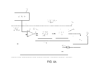
[0073] FIG. 4A shows an example of a power component 114 having a current
feedback loop and a voltage feedback loop, according to some embodiments.
Power
component 114 is configured to provide the current needed to drive one or more
gradient
coils in accordance with a desired pulse sequence. As such, power component
114 is
designed to be a low noise current source that can be precisely controlled to
provide the
commanded current waveform needed to drive the one or more gradient coils to
faithfully
produce the desired gradient magnetic fields. Power component 114 includes a
comparator
301 that receives a current command from controller 106 at its non-inverting
input terminal
and a current feedback signal FB from a current sensor 401 at its inverting
input terminal.
The current command may be a voltage value representing the commanded current.
The
17
CA 02982449 2017-10-11
WO 2016/168249 PCT/US2016/027215
current feedback signal FB may be a voltage value representing the measured
current. In
some embodiments, a high-quality current sensor may be used to provide an
accurate
feedback signal FB, which can improve the accuracy of the gradient coil
current pulses.
[0074] The comparator 301 produces an error signal E (e.g., a voltage)
representing
the difference between the current command and the current feedback signal FB.
Amplifier
circuit 302 amplifies the error signal to produce an amplified error signal
that is provided to
the output stage 303. The output stage 303 drives coil 202 based upon the
amplified error
signal. The current through the coil 202 is measured by current sensor 401,
and a feedback
signal FB is fed back to the comparator 301, as discussed above. The current
feedback loop
thereby causes the current through the coil 202 to be equal to the current
commanded by the
controller 106. In this respect, the power component 114 may operate as a
voltage-controlled
current source. According to some embodiments, a high accuracy, high precision
current
sensor 401 is used to ensure that the current output provided to the gradient
coil accurately
tracks the current commanded by the controller 106. As a result, the current
provided to
power the gradient coil can be held as close to the commanded current as
feasible. The power
component 114 also has a voltage feedback loop that provides the output
voltage of the
output stage 303 to the input of the voltage amplifier circuit 302.
[0075] As illustrated in FIG. 4B, the voltage amplifier circuit 302 may
include an
operational amplifier OA that receives the error signal E at its non-inverting
input and the
voltage feedback signal V FB at its inverting input. The voltage feedback
signal may be
provided to the inverting input of the operational amplifier through a
resistive voltage divider
(e.g., including resistors R1 and R2), which causes the operational amplifier
to amplify the
input voltage based on the ratio of resistance values in the voltage divider.
Any suitable
voltage gain may be used for the voltage amplifier, such a gain of 5-15, by
way of example.
In some embodiments, the voltage gain of the output stage may be one (unity).
[0076] As illustrated in FIG. 4A, in some embodiments, the controller 106
may
provide a command to the output stage 303. The controller 106 may command the
output
stage 303 to produce a power supply voltage suitable for supplying current
needed to perform
a corresponding portion of a pulse sequence. As an example, the command may
cause a
power converter of the output stage to begin ramping up the magnitude of a
power supply
voltage in advance of a gradient coil current pulse. Such a command is
discussed in further
detail below with reference to FIG. 15D.
[0077] In some embodiments, the output stage 303 is configured to be
selectively
powered by a plurality of power supply terminals at different voltages. The
power supply
18
CA 02982449 2017-10-11
WO 2016/168249 PCT/US2016/027215
terminal selected to power the output stage 303 may be chosen depending on the
output
voltage produced by the voltage amplifier. For example, when the power
component is
commanded to produce a relatively high (positive) output voltage the power
component may
be powered from a relatively high (positive) voltage supply terminal, and when
the power
component is commanded to produce a relatively low (positive) output voltage,
the power
component is powered from a relatively low (positive) voltage supply terminal.
Accordingly,
the efficiency of the power component can be improved by reducing the voltage
drop across
its transistor(s) when relatively low output voltage is produced. It should be
appreciated that
any number of supply terminals and voltage levels may be used, as the aspects
are not limited
in this respect. For example, high, mid and low voltage supply terminals (both
positive and
negative) may be used, or an even greater number as suitable for a particular
design and/or
implementation.
[0078] FIG. 5A shows an example of an output stage 303A having an output
Vout,
lout suitable for powering one or more gradient coils of a magnetic resonance
imaging
system. To improve the power efficiency in powering one or more gradient
coils, output
stage 303A can be powered by different supply terminals depending on the
output voltage
Vout. For example, output stage 303A can be powered by a plurality of supply
terminals of a
first polarity (e.g., a plurality of different positive voltages) and/or a
plurality of supply
terminals of a second polarity (e.g., a plurality of different negative
voltages). To facilitate
low noise operation, according to some embodiments, output stage 303A may
include a linear
amplifier 304. According to some embodiment, each of the different supply
terminals
provides a different fixed supply voltage. According to some embodiments, one
or more of
the different supply terminals produce a variable supply voltage, as discussed
in further detail
below.
[0079] In operation, if a positive output voltage is produced at Vout,
switching
circuitry S1 connects the high side power input of linear amplifier 304 to
either the high
voltage terminal +Vhigh or the low voltage terminal +Vlow depending on the
magnitude of
the output voltage. If a relatively high output voltage is to be produced
(e.g., if the output
voltage to be produced exceeds a particular threshold), the switching
circuitry Si connects
the high side power input of linear amplifier 304 to the high voltage terminal
+Vhigh. If a
relatively low output voltage is to be produced (e.g., if the output voltage
to be produced
remains below the particular threshold), the switching circuitry 51 connects
the high side
power input of linear amplifier 304 to the low voltage terminal +Vlow.
Similarly, if a
negative output voltage is produced, switching circuitry S2 connects the low
side power input
19
CA 02982449 2017-10-11
WO 2016/168249 PCT/US2016/027215
of linear amplifier 304 to either the high voltage terminal -Vhigh or the low
voltage terminal -
Vlow depending on the magnitude of the output voltage, as discussed above. Any
suitable
switching circuitry Si and S2 may be used. Such switching circuitry may
include a diode
that is passively switched and/or a transistor that is actively switched.
[0080] In some embodiments, the high-voltage or low-voltage terminals may
be
directly connected to the linear amplifier 304, without an intervening switch
51 or S2. For
example, as shown by the exemplary output stage 303A' illustrated in FIG. 5B,
the high
voltage terminals +Vhigh and ¨Vhigh may be directly connected to the linear
amplifier 304,
and the low voltage terminals +Vlow and ¨Vlow may be connected to the linear
amplifier
304 through respective switches 51 and S2. The linear amplifier 304 may be
designed such
that it is powered by a low voltage supply terminal unless its voltage is
insufficient to supply
the output current, in which case the linear amplifier 304 is powered by the
high voltage
supply terminal. It should be appreciated that the use of +-Vhigh and +-Vlow
is merely
exemplary and any number of voltages levels may be used to provide a desired
output
voltage. For example, one or more intervening voltage levels between +-Vhigh
and +-Vlow,
respectively, may be used to produce the desired voltage levels.
[0081] FIG. 6 shows an example of an output stage 303A having a plurality
of drive
circuits 601-604. Drive circuits 601-604 drive a linear amplifier 304 that
includes a plurality
of transistor circuits 605-608, each including one or more transistors. The
linear amplifier
304 can be connected to the high voltage or low voltage supply terminals
depending on the
output voltage to be produced.
[0082] When a low positive output voltage is to be produced,
transistor(s) 606 are
connected to the low voltage terminal +Vlow via switch circuitry S3.
Transistor(s) 605 are
turned off by drive circuit 601 to isolate the transistors 606 from the high
voltage terminal
+Vhigh. Drive circuit 602 drives transistor(s) 606 as a linear amplifying
element, based on
the input, to produce an amplified output using the low voltage terminal +Vlow
as a source of
current.
[0083] To provide a high positive output voltage, drive circuit 601 turns
on
transistor(s) 605 to connect the high voltage terminal +Vhigh to the
transistors 606. Switch
circuitry S3 may be turned off to isolate transistor(s) 606 from the low
voltage terminal
+Vlow. Drive circuit 602 may drive transistor(s) 606 fully on, such that
transistor(s) 605 are
connected to the output of output stage 303A. Drive circuit 601 drives
transistor(s) 605 as a
linear amplifying element, based on the input, to produce an amplified output
using the high
voltage terminal +Vhigh.
CA 02982449 2017-10-11
WO 2016/168249 PCT/US2016/027215
[0084] Accordingly, the low voltage terminal +Vlow can be used to provide
a low
output voltage and the high voltage terminal +Vhigh can be used to provide a
high output
voltage. A negative output voltage may be provided similarly by drive circuits
603 and 604,
transistor(s) 607 and 608, and switch circuitry S4. When a negative output
voltage is
produced, drive circuits 601 and 602 may turn off transistor(s) 605 and 606.
Similarly, when
a positive output voltage is produced, drive circuits 603 and 604 may turn off
transistor(s)
607 and 608.
[0085] Transistor(s) 606 may operate as a linear amplifying element of
linear
amplifier 304 for low output voltages and transistor(s) 605 may operate as a
linear amplifying
element for high output voltages. In some embodiments, transistor(s) 606 and
605 may be
biased such that for a transition region between low positive output voltages
and high positive
output voltages, transistor(s) 605 and 606 both act as linear amplifying
elements of linear
amplifier 304, i.e., they are neither fully-on nor fully-off. Operating both
transistors 605 and
606 as linear elements during such transitions may facilitate linear amplifier
304 having a
smooth and continuous transfer function. Transistors 607 and 608 may operate
similarly to
transistors 605 and 606 to produce a range of negative output voltages.
[0086] In some embodiments, switch circuitry S3 and S4 may be realized by
diodes
that automatically switch on an off depending on whether the high voltage
terminal is being
utilized. For example, if switch circuitry S3 includes a diode, the anode may
be connected to
the terminal +Vlow and the cathode to transistor(s) 606, such that current can
only flow out
of terminal +Vlow into the output stage 303A. However, the techniques
described herein are
not limited in this respect, as switch circuitry S3 and S4 may be realized
using controlled
switches, such as transistors, or any other suitable switching circuitry.
[0087] In some embodiments, the circuit of FIG. 6 may be used to drive a
gradient
coil using a pulse sequence as shown in FIG. 3. When the output current is
constant, the
output voltage (e.g., 2V) may be produced by sourcing current from the low
voltage terminal
+Vlow. During a transition when the current is changed rapidly, a high output
voltage (e.g.,
100V) may be produced by sourcing current from the high voltage terminal
+Vhigh. Thus,
the high voltage terminal may be used during transitions in the output current
to provide high
output voltages, and the low voltage terminal may be used to provide low
output voltages for
high efficiency.
[0088] According to some embodiments, for example, according to some
pulse
sequences, the high voltage terminal(s) may only need to be used for a
relatively short period
of time, so that transistor(s) 605 (and 608) may be conducting for only a
relatively small duty
21
CA 02982449 2017-10-11
WO 2016/168249 PCT/US2016/027215
cycle. Thus, in some embodiments, transistor(s) 605 (and 608) may be reduced
in size,
and/or the number of transistors connected in parallel may be reduced, with
respect to
transistors 606 (or 607), as transistor(s) 605 (and 608) will have time to
dissipate heat
between transitions in the gradient coil current.
[0089] In some embodiments, drive circuits 601 and 604 may be designed to
provide
time-limited output signals. Providing time-limited output signals may ensure
that
transistor(s) 605 and/or 608 are turned on only temporarily and not turned on
to drive a
steady state current. Such a technique may be advantageous if transistor(s)
605 or 608 are
designed to conduct for only relatively short periods of time, as it can
prevent excessive
power dissipation by transistor(s) 605 or 608.
[0090] FIG. 7 shows a block diagram of drive circuitry 601 and 602,
according to
some embodiments. Drive circuitry 601 includes a drive transistor 703A for
driving
transistor(s) 605. Drive circuitry 602 includes a drive transistor 703B for
driving transistor(s)
606.
[0091] Drive circuitry 601 and 602 may include one or more bias circuits
701 for
producing a DC bias on the input voltage provided to the drive transistors
703A and 703B. In
some embodiments, the bias circuit(s) 701 may bias drive transistors 703A
and/or 703B
slightly below their turn-on voltages. The inventors have recognized and
appreciated that
biasing the drive transistors slightly below their turn-on voltages can reduce
or eliminate
thermal runaway. Advantageously, such a biasing technique may not reduce the
linearity of
the output stage 303A. If an operational amplifier OA of voltage amplifier
circuit 302 has a
sufficiently high speed, it can respond fast enough to accurately control the
output voltage of
the output stage despite biasing the drive transistors slightly below their
turn-on voltages.
[0092] In some embodiments, drive circuitry 601 may include a timing
circuit that
causes drive circuit 601 to produce a time-limited output. Any suitable timing
circuit may be
used. In the example of FIG. 7, a timing circuit 702 is connected to the input
of output stage
303A via bias circuit 701, and limits the amount of time that an input can be
provided to the
drive transistor 703A.
[0093] In some embodiments, the timing circuit 702 may be an RC circuit
that has an
output voltage that decays over time, and turns off drive transistor 703A when
the output of
the timing circuit 702 falls below the turn on voltage of the drive transistor
703A. The time
that transistor(s) 605 are turned on is limited based on the RC time constant
of the RC circuit.
However, the techniques described herein are not limited to implementing the
timing circuit
using an RC circuit, as any suitable timing circuitry may be used, including
analog and/or
22
CA 02982449 2017-10-11
WO 2016/168249 PCT/US2016/027215
digital circuitry. In some embodiments, drive circuits 603 and 604 may be
implemented
similarly to drive circuits 602 and 601, respectively, for negative input and
output voltages.
[0094] FIG. 8 shows an example implementation of the drive circuits of
FIG. 7, in
accordance with some embodiments of the technology described herein. As shown
in FIG. 8,
in some embodiments, the bias circuit 701 may be realized by a Zener diode in
series with a
resistor R2, connected between the high voltage terminal +Vhigh and a lower
voltage DC
terminal (e.g., -Vhigh) below the voltage of +Vhigh. In some embodiments, the
bias circuit
701 may include additional circuitry between the high voltage terminal +Vhigh
and the lower
voltage DC terminal to provide a DC path for current to flow between them and
establish a
suitable bias voltage. In some embodiments, the bias circuit 701 may include
another Zener
diode and resistor in series with the Zener diode and resistor shown in FIG.
8, for providing
bias voltage(s) to the low-side drive circuits 603 and 604. However, this is
merely by way of
example, as any suitable bias circuit may be used. FIG. 8 also illustrates an
example of a
timing circuit 702 realized as an RC circuit having a capacitor Cl and a
resistor Rl. Again,
this is merely one example of a timing circuit, as other configurations of
timing circuits may
be used. Drive transistors 703A and 703B are shown as being realized by
bipolar junction
transistors. However, the techniques described herein are not limited in this
respect, as the
drive transistors may be realized by any type of transistors. Transistor
circuits 605 and 606
are shown as MOSFETs, in this example. However, the transistor circuits 605
and 606 may
be realized by any type of transistors. In some embodiments, transistor
circuits 605 and/or
606 may have a plurality of transistors connected in parallel. As discussed
above, switch
circuitry S3 may be realized as a diode, as shown in FIG. 8. However, as
discussed above,
the techniques described herein are not limited in this respect, as in some
embodiments
switch circuitry S3 may be realized by a transistor.
[0095] FIG. 9 shows another example of a technique for implementing a
timing
circuit. The inventors have recognized and appreciated that if switch S3 is
realized by a
diode, the voltage across the diode can be used as a trigger for a timing
circuit to limit the
amount of time that transistor(s) 605 are turned on. When a low output voltage
is produced
by linear amplifier 304, the diode is forward biased and conducting. When the
linear
amplifier 304 produces a high output voltage, transistor(s) 605 turn on and
the diode switches
from being forward biased to being reverse biased. The reverse bias voltage
can be sensed by
timing circuit 902 as an indication that transistor(s) 605 are being turned
on. In the example
of FIG. 9, the voltage across the diode is provided as an input to timing
circuit 902, which
produces an inhibit signal to inhibit the operation of drive circuit 601 after
a period of time,
23
CA 02982449 2017-10-11
WO 2016/168249 PCT/US2016/027215
thereby limiting the amount of time that transistor(s) 605 are turned on.
Timing circuit 904
may operate similarly in order to inhibit the operation of drive circuit 604
after transistor(s)
608 have been conducting for a period of time.
[0096] FIG. 10 shows an example of timing circuits 902 and 904 realized
by an RC
circuit and a bipolar transistor. In timing circuit 902, for example, once the
diode is reverse
biased after a period of time the output of the RC circuit rises to a level
where the bipolar
transistor turns on. When the bipolar transistor turns on, the input of the
drive circuit 601 is
pulled down to +Vlow, which turns off the drive circuit 601 and transistor(s)
605.
[0097] Although FIGS. 6, 9 and 10 show a "double-ended" linear amplifier
304 that
may produce a positive output voltage or a negative output voltage, the
techniques described
herein are not limited in this respect, as in some embodiments a single-ended
linear amplifier
may be used. FIG. 11 shows an example of an output stage 303B including a
single-ended
linear amplifier 305 that produces only positive output voltages. FIG. 11
schematically
illustrates that the single-ended linear amplifier 305 may be connected to a
high positive
voltage terminal +Vhigh or a low positive voltage terminal +Vlow by switch 51,
depending
on the output voltage to be produced. The output stage 303B may be implemented
using the
drive circuits 601, 602, transistor(s) 605 and 606, and associated switch
circuit S3 discussed
above, in some embodiments.
[0098] The output stage 303B may provide a positive output voltage or a
negative
output voltage to a load using a polarity-switching circuit 1104. In the
example of FIG. 11,
polarity-switching circuit 1104 is realized using an H-bridge including
switches S5-S8. A
positive voltage may be provided to the load by turning on switches S5 and S8
and turning
off switches S6 and S7. A negative voltage may be provided to the load by
turning on
switches S6 and S7 and turning off switches S5 and S8. In some embodiments,
the control
circuit (not shown) may control switches S5-S8 to produce an output voltage of
a suitable
polarity. The polarity may be determined by examining the polarity of the
current command,
the error signal E, or any other suitable signal.
[0099] As discussed above, conventional switching converters can
introduce a
significant amount of switching noise into the system because they switch at
frequencies in
the range of tens to hundreds of kHz. Such switching noise can interfere with
imaging
because it is in the same frequency range as MR signals desired to be
detected. The inventors
have recognized that a power converter having a switching frequency above the
Larmor
frequency of interest does not interfere with imaging to a significant degree.
Accordingly, in
some embodiments, power component 114 may include a switching power converter
1202
24
CA 02982449 2017-10-11
WO 2016/168249 PCT/US2016/027215
that is designed to switch at a relatively high switching frequency, above the
Larmor
frequency of interest, as shown in FIG. 12. In some embodiments, the switching
frequency
may be higher than 1 MHz, higher than 10 MHz, higher 30 MHz or higher than 300
MHz.
[0100] As discussed above, the inventors have appreciated that providing
variable
voltage supply terminals facilitates efficient powering of one or more
gradient coils of a
magnetic resonance imaging system (e.g., a low-field MRI system). In some
embodiments,
the output stage may be powered by one or more or more variable voltage supply
terminals
that are controlled to produce supply voltages close to the desired output
voltage. Providing
such a variable voltage supply terminal can improve the efficiency of the
output stage by
limiting the voltage drop across the linear amplifier.
[0101] FIG. 13 shows an embodiment of an output stage 303C that may be
powered
by a variable voltage positive supply terminal and a variable voltage negative
supply
terminal. The voltages of the supply terminals can be varied depending on the
output voltage
to reduce the voltage drop across the transistor(s) of the linear amplifier
306, thus facilitating
efficient powering of gradient coil(s) to produce magnetic fields according to
a desired pulse
sequence. In some embodiments, the voltage of the positive voltage terminal
and/or the
negative voltage terminal may be provided by power converters 1304 and/or
1306,
respectively. The variable output voltages of the power converters 1304 and/or
1306 may be
controlled by a controller 1308 based on the desired output voltage of output
stage 303C to
maintain the voltages of the positive voltage terminal and/or the negative
voltage terminal
slightly above (or below, respectively) the output voltage of the output
stage, thereby
reducing the voltage drop across the transistor(s) of the linear amplifier.
[0102] According to some embodiments, controller 1308 controls the
variable output
voltages of the power converters 1304 and/or 1306 based on the output voltage
of linear
amplifier 306. However, the variable output voltages may be controlled in
other ways and/or
in different relationship to the desired output voltage of output stage 303C.
For example, the
variable output voltages may be controlled based on the command (e.g., current
command)
provided to linear amplifier 306. As discussed in the foregoing, a controller
may be
configured to command the linear amplifier to produce output sufficient to
drive one or more
gradient coils of a magnetic resonance imaging system in accordance with a
desired pulse
sequence. As such, controller 1308 may be configured to control the variable
output voltages
of the power converters 1304 and/or 1306 so that the output voltages provided
to the linear
amplifier are sufficient, without being too excessive and therefore
inefficient, to allow the
linear amplifier to produce output to power the one or more gradient coils in
accordance with
CA 02982449 2017-10-11
WO 2016/168249 PCT/US2016/027215
the desired pulse sequence. Control of the power converters 1304 and 1306 may
be
performed in any suitable way, such as by controlling their duty ratio, their
frequency, or any
other control parameter that can control the output voltage of the power
converters. In some
embodiments, power converters 1304 and 1306 of FIG. 13 may be switching power
converters designed to switch at a relatively high switching frequency, above
the Larmor
frequency of interest, as discussed above. However, any suitable power
converter may be
used, as the aspects are not limited in this respect.
[0103] In some embodiments, both high and low voltage supply terminals
(e.g.,
+Vhigh and +Vlow) may power the linear amplifier, as illustrated in FIGS. 5,
6, and 11, and
the voltage of the low voltage supply terminal, the high voltage supply
terminal, both, or any
supply terminal provided may be variable. FIG. 14A shows an embodiment of an
output
stage 303D similar to FIG. 5A with variable low voltage supply terminals.
Rather than
having low voltage terminals +Vlow and ¨Vlow at fixed voltages, FIG. 14A shows
that
+Vlow and ¨Vlow can have variable voltages. In some embodiments, the variable
voltages
of +Vlow and ¨Vlow may be provided by power converters 1403 and 1404,
respectively. In
some embodiments, power converters 1403 and 1404 may be switching power
converters
designed to switch at a relatively high switching frequency, above the Larmor
frequency of
interest, as discussed above. When a relatively low output voltage is to be
produced (e.g., in
the steady state), current is sourced from the low voltage supply terminals
+Vlow or ¨Vlow.
The output voltages +Vlow or ¨Vlow of the power converters 1403 or 1404 may be
controlled by controller 1308 based on the desired output voltage Vout of
linear amplifier 304
to maintain the voltages of the low voltage supply terminals +Vlow or ¨Vlow
slightly above
(or below, respectively) the output voltage of the output stage, thereby
reducing the voltage
drop across the transistor(s) of the linear amplifier in the steady state and
reducing power
dissipation. When a relatively high output voltage is to be produced, current
may be sourced
from the high voltage terminals +Vhigh or +Vlow, which may have fixed
voltages.
[0104] +Vhigh may be a separate terminal from the power supply terminal
Vhigh Supply that supplies power to power converter 1403, as illustrated in
FIG. 14A, or
may be the same terminal as Vhigh Supply, as illustrated in FIG. 14B. In FIG.
14B, an
example is shown of an output stage 303E in which +Vhigh is provided from the
power
supply terminal Vhigh Supply and ¨Vhigh is provided from the power supply
terminal
Vlow Supply that provides power to power converter 1404. Providing +Vhigh
and/or ¨
Vhigh from the existing power supply terminals can avoid the need to produce
additional
26
CA 02982449 2017-10-11
WO 2016/168249 PCT/US2016/027215
power supply voltages, which can simplify the design and implementation of the
output
stage.
[0105] FIG. 15A shows an example of a gradient coil current waveform,
according to
some embodiments. The gradient coil current is initially zero, then rapidly
ramps up to 10A
in 0.1 ms. The current remains at 10A for a period of time, then drops back to
OA. The
current remains at OA for a period of time before rapidly ramping up to 20A in
0.2 ms. The
current remains at 20A for a period of time, then drops back to OA. It should
be appreciated
that the amp values and time intervals are merely exemplary for the purposes
of illustration,
and any suitable values may be used.
[0106] FIG. 15B shows the rising transition of the gradient coil current
from OA to
10A, the voltage 1502 needed for driving the gradient coil, the voltage of the
high voltage
supply terminal +Vhigh and the low voltage supply terminal +Vlow. During the
transition,
current is sourced from the high voltage supply terminal +Vhigh in order to
provide a high
voltage to the gradient coil to quickly ramp up its current. As the transition
occurs, the power
converter 1403 begins to ramp up the voltage of the low voltage supply
terminal +Vlow from
¨0V to a voltage slightly higher than the output voltage necessary to drive
the gradient coil
with a steady state current of 10A. Once the steady state current of 10A is
reached, current is
sourced from the low voltage supply terminal +Vlow in order to provide high
efficiency in
the steady state.
[0107] FIG. 15C shows the rising transition of the gradient coil current
from OA to
20A, the gradient coil voltage, and the voltage of the high voltage supply
terminal +Vhigh
and the low voltage supply terminal +Vlow. During the transition to 20A, as
with the
transition to 10A, current is sourced from the high voltage supply terminal
+Vhigh in order to
provide a high voltage to the gradient coil to quickly ramp up its current. As
the transition
occurs, the power converter 1403 begins to ramp up the voltage of the low
voltage supply
terminal +Vlow from ¨0V to a voltage slightly higher than the output voltage
necessary to
drive the gradient coil with a steady state current of 20A. Once the steady
state current of
20A is reached, current is sourced from the low voltage supply terminal +Vlow.
[0108] Since the voltage of the low voltage supply terminal +Vlow can be
varied, it
can be set slightly above the output voltage needed for different steady state
current levels.
This can improve the efficiency over the case of using a low voltage supply
terminal +Vlow
having a fixed voltage, as a fixed voltage would need to be designed to handle
the maximum
steady state current, which may be a higher voltage than necessary for driving
lower steady
state currents, which can decrease efficiency. As an example, if the +Vlow is
set high
27
CA 02982449 2017-10-11
WO 2016/168249 PCT/US2016/027215
enough to supply a 20A steady state gradient coil current, such a voltage is
higher than
necessary to supply a 10A steady state gradient coil current, which results in
increased
voltage drop across the linear amplifier transistor(s) when supplying a 10A
steady state
gradient coil current, and higher power dissipation occurs than is necessary.
A variable
voltage can be set at or near the minimum voltage necessary to supply the
commanded steady
state gradient coil current, which improves efficiency.
[0109] FIG. 15D shows a current command, gradient coil current, the
voltage 1502 of
the gradient coil needed to supply the current, and several different
transition waveforms of
the voltage +Vlow. Transition waveform 1504 shows an idealized transition in
which the
voltage of +Vlow starts ramping up in response to the rising edge of the
gradient coil current
command, and reaches the steady state value of +Vlow at the same time that the
steady state
gradient coil current (and voltage values) are reached. However, the inventors
have
recognized and appreciated that there may be factors preventing the voltage
+Vlow from
reaching a sufficient voltage level in time for the terminal +Vlow to supply
the steady state
current. Transition waveform 1506 shows a more realistic transition of +Vlow,
which has a
period of latency (delay) in responding to the gradient coil current command.
As shown in
FIG. 15D, the transition waveform 1506 starts ramping up only after a period
of time
following the rising edge of the current command. The slope of the transition
waveform
1506 may be limited, as the power converter 1403 may have an output filter
(e.g., a capacitor)
that limits the speed with which power converter 1403 can change the voltage
of +Vlow. As
a result, the transition waveform 1506 may not reach a sufficient voltage
level by the time the
steady state gradient coil current and voltage are reached, which may result
in the low voltage
supply terminal +Vlow being unable to supply the steady state current, at
least temporarily.
[0110] To address this, in some embodiments, the power converter 1403 (or
1404)
may begin ramping up the magnitude of the voltage of +Vlow (or ¨Vlow) before
the rising
edge of the gradient coil current command. FIG. 15D shows a transition
waveform 1508 for
+Vlow that starts ramping up before the rising edge of the gradient coil
current command.
To begin the transition prior to the rising edge of the gradient coil current
command,
controller 1308 may receive information from controller 106 regarding an
upcoming gradient
coil current pulse, and begin ramping up the magnitude of the voltage of +Vlow
(or ¨Vlow)
in anticipation of the current pulse. This information may be provided from
controller 106 to
controller 1308 in any suitable way. As an example, the controller 106 may
analyze the
currently selected gradient coil pulse sequence, determine a power supply
voltage level
suitable to supply the steady state gradient coil current for the next current
pulse, and send a
28
CA 02982449 2017-10-11
WO 2016/168249 PCT/US2016/027215
voltage command to controller 1308 in advance of an anticipated current
command. The
power converter 1403 (or 1404) may then respond to the received voltage
command and
begin ramping +Vlow (or ¨Vlow) to the commanded voltage value. As another
example of
providing the information to the controller 1308, the controller 106 may send
the currently
selected pulse sequence or a portion of the pulse sequence to controller 1308.
Controller
1308 may then analyze the pulse sequence and send commands to the power
converter 1403
(or 1404) to start ramping the voltage +Vlow (or ¨Vlow) in advance of a
gradient coil current
pulse. In the example of FIG. 15D, the power converter 1403 starts ramping up
the voltage
of +Vlow in response to a voltage command provided by controller 106 to
controller 1308 in
advance of the rising edge of the current command As a result, the transition
waveform 1508
reaches the level of +Vlow sufficient to supply the steady state current by
the time the steady
state current level is reached.
[0111] FIG. 16A shows an embodiment of an output stage 303F with a single-
ended
linear amplifier similar to that of FIG. 11, with a variable low voltage
supply terminal +Vlow.
As with the embodiment of FIG. 14A, the power converter 1403 supplies a
variable voltage
to the low voltage supply terminal +Vlow that can be set slightly above the
voltage needed to
supply the commanded steady state gradient coil current.
[0112] As discussed above in connection with FIGS. 14A and FIG. 14B, the
high
voltage supply terminal +Vhigh may be a separate terminal from the power
supply terminal
Vhigh Supply, as illustrated in FIG. 16A, or may be the same terminal as Vhigh
Supply, as
illustrated in FIG. 16B. In FIG. 16B, an example of an output stage 303G is
shown in which
+Vhigh is provided from the power supply terminal Vhigh Supply. Providing the
voltage
+Vhigh from the existing power supply terminal Vhigh Supply can avoid the need
to
produce additional power supply voltages, which can simplify the design and
implementation
of the output stage.
[0113] In some embodiments, both the low voltage supply terminal(s) and
the high
voltage supply terminal(s) may have variable voltages. For example, the
embodiments of
FIGS. 14 or 11 may be modified such that the high voltage supply terminals
+Vhigh and/or
-Vhigh are variable voltages produced by power converters. Such power
converters may be
similar to power converters 1403 and 1404, and may be controlled by the
controller 1308, as
well. Such an embodiment can be used for any suitable type of imaging, and may
be
particularly useful for diffusion weighted imaging, for example, where
relatively large
currents may be needed (e.g., 40A, 50A, 70A, 90A or more, or any values there
between).
29
CA 02982449 2017-10-11
WO 2016/168249 PCT/US2016/027215
[0114] In some embodiments, one or more additional power supply terminals
may
power the linear amplifier. For example, a third power supply terminal may be
provided that
has a voltage higher than the high voltage supply terminal +Vhigh (e.g., at
least 5 times
higher or at least 10 times higher, and even as high as 20 or 30 times higher
or more, or in
any range between such values). Adding a third supply terminal may help
improve efficiency
in the case where a wide range of voltages need to be produced. Any number of
power
supply terminals may be provided, as the techniques described herein are not
limited in this
respect.
[0115] Having thus described several aspects and embodiments of the
technology set
forth in the disclosure, it is to be appreciated that various alterations,
modifications, and
improvements will readily occur to those skilled in the art. Such alterations,
modifications,
and improvements are intended to be within the spirit and scope of the
technology described
herein. For example, those of ordinary skill in the art will readily envision
a variety of other
means and/or structures for performing the function and/or obtaining the
results and/or one or
more of the advantages described herein, and each of such variations and/or
modifications is
deemed to be within the scope of the embodiments described herein. Those
skilled in the art
will recognize, or be able to ascertain using no more than routine
experimentation, many
equivalents to the specific embodiments described herein. It is, therefore, to
be understood
that the foregoing embodiments are presented by way of example only and that,
within the
scope of the appended claims and equivalents thereto, inventive embodiments
may be
practiced otherwise than as specifically described. In addition, any
combination of two or
more features, systems, articles, materials, kits, and/or methods described
herein, if such
features, systems, articles, materials, kits, and/or methods are not mutually
inconsistent, is
included within the scope of the present disclosure.
[0116] The above-described embodiments can be implemented in any of
numerous
ways. One or more aspects and embodiments of the present disclosure involving
the
performance of processes or methods may utilize program instructions
executable by a device
(e.g., a computer, a processor, or other device) to perform, or control
performance of, the
processes or methods. In this respect, various inventive concepts may be
embodied as a
computer readable storage medium (or multiple computer readable storage media)
(e.g., a
computer memory, one or more floppy discs, compact discs, optical discs,
magnetic tapes,
flash memories, circuit configurations in Field Programmable Gate Arrays or
other
semiconductor devices, or other tangible computer storage medium) encoded with
one or
more programs that, when executed on one or more computers or other
processors, perform
CA 02982449 2017-10-11
WO 2016/168249 PCT/US2016/027215
methods that implement one or more of the various embodiments described above.
The
computer readable medium or media can be transportable, such that the program
or programs
stored thereon can be loaded onto one or more different computers or other
processors to
implement various ones of the aspects described above. In some embodiments,
computer
readable media may be non-transitory media.
[0117] The terms "program" or "software" are used herein in a generic
sense to refer
to any type of computer code or set of computer-executable instructions that
can be employed
to program a computer or other processor to implement various aspects as
described above.
Additionally, it should be appreciated that according to one aspect, one or
more computer
programs that when executed perform methods of the present disclosure need not
reside on a
single computer or processor, but may be distributed in a modular fashion
among a number of
different computers or processors to implement various aspects of the present
disclosure.
[0118] Computer-executable instructions may be in many forms, such as
program
modules, executed by one or more computers or other devices. Generally,
program modules
include routines, programs, objects, components, data structures, etc. that
perform particular
tasks or implement particular abstract data types. Typically the functionality
of the program
modules may be combined or distributed as desired in various embodiments.
[0119] Also, data structures may be stored in computer-readable media in
any suitable
form. For simplicity of illustration, data structures may be shown to have
fields that are
related through location in the data structure. Such relationships may
likewise be achieved
by assigning storage for the fields with locations in a computer-readable
medium that convey
relationship between the fields. However, any suitable mechanism may be used
to establish a
relationship between information in fields of a data structure, including
through the use of
pointers, tags or other mechanisms that establish relationship between data
elements.
[0120] When implemented in software, the software code can be executed on
any
suitable processor or collection of processors, whether provided in a single
computer or
distributed among multiple computers.
[0121] Further, it should be appreciated that a computer may be embodied
in any of a
number of forms, such as a rack-mounted computer, a desktop computer, a laptop
computer,
or a tablet computer, as non-limiting examples. Additionally, a computer may
be embedded
in a device not generally regarded as a computer but with suitable processing
capabilities,
including a Personal Digital Assistant (PDA), a smartphone or any other
suitable portable or
fixed electronic device.
31
CA 02982449 2017-10-11
WO 2016/168249 PCT/US2016/027215
[0122] Also, a computer may have one or more input and output devices.
These
devices can be used, among other things, to present a user interface. Examples
of output
devices that can be used to provide a user interface include printers or
display screens for
visual presentation of output and speakers or other sound generating devices
for audible
presentation of output. Examples of input devices that can be used for a user
interface
include keyboards, and pointing devices, such as mice, touch pads, and
digitizing tablets. As
another example, a computer may receive input information through speech
recognition or in
other audible formats.
[0123] Such computers may be interconnected by one or more networks in
any
suitable form, including a local area network or a wide area network, such as
an enterprise
network, and intelligent network (IN) or the Internet. Such networks may be
based on any
suitable technology and may operate according to any suitable protocol and may
include
wireless networks, wired networks or fiber optic networks.
[0124] Also, as described, some aspects may be embodied as one or more
methods.
The acts performed as part of the method may be ordered in any suitable way.
Accordingly,
embodiments may be constructed in which acts are performed in an order
different than
illustrated, which may include performing some acts simultaneously, even
though shown as
sequential acts in illustrative embodiments.
[0125] All definitions, as defined and used herein, should be understood
to control
over dictionary definitions, definitions in documents incorporated by
reference, and/or
ordinary meanings of the defined terms.
[0126] The indefinite articles "a" and "an," as used herein in the
specification and in
the claims, unless clearly indicated to the contrary, should be understood to
mean "at least
one."
[0127] The phrase "and/or," as used herein in the specification and in
the claims,
should be understood to mean "either or both" of the elements so conjoined,
i.e., elements
that are conjunctively present in some cases and disjunctively present in
other cases.
Multiple elements listed with "and/or" should be construed in the same
fashion, i.e., "one or
more" of the elements so conjoined. Other elements may optionally be present
other than the
elements specifically identified by the "and/or" clause, whether related or
unrelated to those
elements specifically identified. Thus, as a non-limiting example, a reference
to "A and/or
B", when used in conjunction with open-ended language such as "comprising" can
refer, in
one embodiment, to A only (optionally including elements other than B); in
another
32
CA 02982449 2017-10-11
WO 2016/168249 PCT/US2016/027215
embodiment, to B only (optionally including elements other than A); in yet
another
embodiment, to both A and B (optionally including other elements); etc.
[0128] As used herein in the specification and in the claims, the phrase
"at least one,"
in reference to a list of one or more elements, should be understood to mean
at least one
element selected from any one or more of the elements in the list of elements,
but not
necessarily including at least one of each and every element specifically
listed within the list
of elements and not excluding any combinations of elements in the list of
elements. This
definition also allows that elements may optionally be present other than the
elements
specifically identified within the list of elements to which the phrase "at
least one" refers,
whether related or unrelated to those elements specifically identified. Thus,
as a non-limiting
example, "at least one of A and B" (or, equivalently, "at least one of A or
B," or, equivalently
"at least one of A and/or B") can refer, in one embodiment, to at least one,
optionally
including more than one, A, with no B present (and optionally including
elements other than
B); in another embodiment, to at least one, optionally including more than
one, B, with no A
present (and optionally including elements other than A); in yet another
embodiment, to at
least one, optionally including more than one, A, and at least one, optionally
including more
than one, B (and optionally including other elements); etc.
[0129] Also, the phraseology and terminology used herein is for the
purpose of
description and should not be regarded as limiting. The use of "including,"
"comprising," or
"having," "containing," "involving," and variations thereof herein, is meant
to encompass
the items listed thereafter and equivalents thereof as well as additional
items.
[0130] In the claims, as well as in the specification above, all
transitional phrases
such as "comprising," "including," "carrying," "having," "containing,"
"involving,"
"holding," "composed of," and the like are to be understood to be open-ended,
i.e., to mean
including but not limited to. Only the transitional phrases "consisting of'
and "consisting
essentially of' shall be closed or semi-closed transitional phrases,
respectively.
33