Note: Descriptions are shown in the official language in which they were submitted.
COMPACT RESOLVER PRE-AMPLIFICATION ASSEMBLY (RPA) MODULE
Field of Invention
The present invention relates generally to accurate robotic arm joint
lo absolute position telemetry.
Background
Mars Science Laboratory (MSL) arms on Opportunity and Spirit both use
potentiometers to report robotic arm joint position. A potentiometer is a low-
accuracy feedback device.
The MSL arm on Curiosity was the first Mars arm to transition away from
potentiometers and implemented resolvers to provide joint position feedback.
The system experienced noise issues, and no pre-amp electronics were
incorporated because that arm could not support the size and mass of pre-amp
electronics available at that time. Without pre-amp electronics, the resolver
output position telemetry became unusable. Motor encoders (which did not
support joint output sensing) were installed to support joint position
knowledge.
The NASA Goddard Flight Telerobotic Servicer (FTS) arms incorporated
resolver-based position sensors to report joint position. These arms were
planned for use on the International Space Station (ISS), but they were never
flown.
The German Aerospace Center (known as DLR) built and demonstrated
the Robot Technology Experiment (ROTEX), a small robotic arm which
incorporated an early version of joint position sensing, in a Spacelab
experimentation rack. DLR's Robotics Component Verification on the ISS
(ROKVISS) was a 2-DOE arm which built upon lessons learned from ROTEX,
1
Date Recue/Date Received 2022-07-29
CA 02985817 2017-11-10
WO 2016/183343
PCT/US2016/032145
implementing magnetoresistive encoders to report joint position. Both ROTEX
and ROKVISS were used in the LEO environment.
The European Robotic Arm (ERA), similar to the Space Station Remote
Manipulator System (SSRMS) and JEMSRMS, was a large, relocatable,
symmetrical arm built for use on the Russian Multipurpose Laboratory module of
the ISS. The ERA will work with the Russian airlock to transfer small payloads
directly from inside to outside the ISS. It will be teleoperated by astronauts
from
inside or outside the ISS. The ERA is designed and assembled by Dutch Space.
The ERA joint position is determined from the difference between a joint
position
set point and the joint position measurements of an optical position sensor.
It
also uses the difference between a velocity set point and motor velocity
position
measurement provided by a resolver.
Summary of Invention
Space-qualified absolute encoders come from primarily one source, and
as a result, are very expensive and long-lead. They are typically larger in
size,
more fragile, and have radiation concerns at GEO environment levels. The joint
position sensing systems mentioned above are not able to support the same
combination of environmental, performance, and packaging requirements
exemplary modules provide.
The Front-end Robotics Enabling Near-term Demonstration (FREND)
MKII robotic arm requires high accuracy of joint position knowledge and thus
incorporates an exemplary Resolver Preamp Assembly (RPA) module and
Inductosyn absolute position sensing system. Exemplary RPA modules provide
a small form factor package with parts that are radiation-tolerant in the GEO-
environment radiation, so it may be co-located at each joint to maintain
robotic
arm dexterity, thus allowing the arm to meet performance requirements.
The Resolver Preamp Assembly (RPA) module must receive and amplify
sensitive Inductosyn signals while reducing any potential noise amplification
in
order to maintain signal integrity and provide accurate joint position. To
reduce
noise amplification in the system, the RPA module needs to be located in close
proximity of the Inductosyn at each joint and thus compact in size to maintain
joint range of motion and robotic arm dexterity. The Compact RPA Module is
2
planned to support missions at geosynchronous orbits thus must also be
designed to meet the electromagnetic interference and radiation environmental
requirements.
According to one aspect of the invention, a compact resolver pre-
amplification assembly has first and second printed circuit boards. The
circuit
boards include an interface with an N/N-1 resolver and a resolver-to-digital
converter, a first signal path including circuitry configured to drive a field
director
and Inductosyn primaries, wherein the first signal path is configured to
receive a
differential signal from robotic control electronics, condition the signal,
and then
amplify the signal, driving the field director and Inductosyn primaries; a
second
signal path including circuitry configured to amplify, condition, and output,
to a
differential output, sine (Sin) and cosine (Cos) outputs from a field director
secondary; and a third signal path including circuitry configured to amplify,
condition, and convert, to a differential signal, sine and cosine outputs from
an
Inductosyn secondary. The first and second circuit boards are contained in a
single package configured for mounting on a robotic joint, and low level
sensitive
signals are separated from high level excite signals by locating sensitive
signals
on the first board and excite signals on the second board.
Optionally, the compact resolver pre-amplification assembly of the present
invention includes an excite drive circuit having a differential line
receiver, a
phase adjustment circuit, and a power output stage configured to drive the
lnductosyn primary.
Optionally, the compact resolver pre-amplification assembly includes
recovery amplifiers configured to provide high gain, amplifying recovered Sin
and
Cos signals for input to a resolver-to-digital converter.
Optionally, the recovery amplifiers include three amplifier stages and a
unity gain differential line drive circuit driving amplified signals to the
resolver-to-
digital converter.
Optionally, the first gain stage includes a 10:1 input transformer
configured to provide galvanic isolation and high common-mode rejection and
RF filtering, reducing the coupling of anomalous signals into the amplifiers.
Optionally, the transformer has a low primary resistance to minimize
Johnson noise and is housed in a magnetic shield.
3
Date Recue/Date Received 2022-07-29
CA 02985817 2017-11-10
WO 2016/183343 PCT/US2016/032145
Optionally the compact resolver pre-amplification assembly includes a line
driver circuit including inverting and non-inverting unity gain amplifiers
configured
to provide a differential signal output to interface with resolver-to-digital
converter
receivers and interconnecting cables. The line driver circuit is configured to
provide a low output impedance while isolating the driver circuit from the
cable
capacitance to ensure stability.
Optionally, the line driver circuit provides a DC feedback path taken from
outside of an isolation resistor lowering the output impedance, and an AC
feedback path taken directly at an op-amp output ensuring high frequency
stability.
Optionally, the compact resolver pre-amplification assembly includes
power supply decoupling capacitors on input power rails.
Optionally, the compact resolver pre-amplification assembly includes a
bulk RC filter configured to provide a second stage of filtering for all high
gain
amplifier stages; and an individual RC filter for each op-amp of the recovery
amplifiers.
Optionally, the printed circuit boards include multiple layers shielding and
isolating signals.
Optionally, the printed circuit boards include circuit functions and routing
arranged to provide minimal signal coupling with adjacent circuits.
Optionally, individual layers include isolated ground planes and guard
rings to isolate sensitive circuitry.
Optionally, Inductosyn 127x and 128x SIN and COS signals are treated
as four separate analog channels and are segregated to separate pre-amp
islands each associated with respective segmented underlying ground planes,
preventing inner channel currents from coupling with one another.
Optionally, the input signal path is routed in a sub-layer surrounded by
segmented ground planes thereby reducing noise coupling, and downstream of
the pre-amp, the segmented ground planes are joined as one analog ground
plane in a star ground.
Optionally, isolation between the excite drive signal and the high-gain
amplifiers exceeds 50 dB while providing gains that range from 3000 to 5000.
Optionally, isolation between sine and cosine amplifiers exceeds 60dB.
4
CA 02985817 2017-11-10
WO 2016/183343 PCT/US2016/032145
Optionally, the first board includes twelve layers. Layer 2 includes a first
segmented ground plane; layer 3 includes two sensitive signal routings; layer
4
includes a second segmented ground plane; layer 9 includes a third segmented
ground plane; layer 10 includes two sensitive signal routings separate from
the
signal routings on layer 3; and layer 11 includes a fourth segmented ground
plane.
Optionally, the first board includes twelve layers and layer 3 includes two
sensitive signal routings, each routing being enclosed by a respective guard
ring,
shielding input signals upstream of transformers; and layer 10 includes two
sensitive signal routings separate from the signal routings on layer 3, each
routing being enclosed by a respective guard ring, shielding input signals
upstream of transformers.
Optionally, the first board includes twelve layers and layers 5, 6, 7, and 8
each include a power plane separated into two channels that are connected at
one point, thereby preventing noise from flowing between adjacent circuits.
Optionally, the compact resolver pre-amplification assembly is in
combination with a robotic arm and a second compact resolver pre-amplification
assembly. The compact resolver pre-amplification assemblies are mounted on
and receive information from respective joints of the robotic arm.
The foregoing and other features of the invention are hereinafter
described in greater detail with reference to the accompanying drawings.
Brief Description of the Drawings
FIG. 1 shows a robotic arm equipped with an exemplary RPA module.
FIG. 2 shows a functional block diagram of an exemplary RPA module.
FIG. 3 shows a block diagram of an exemplary RPA module.
FIG. 4 shows an excite drive portion of an exemplary RPA module.
FIG. 5 shows an Inductosyn recover amplifiers portion of an exemplary
RPA module.
FIG. 6 shows a line driver portion of an exemplary RPA module.
FIG. 7 shows a combined amplifier line driver circuit portion of an
exemplary RPA module.
5
CA 02985817 2017-11-10
WO 2016/183343 PCT/US2016/032145
FIG. 8 shows a first and second stage power supply decoupling portion of
an exemplary RPA module.
FIG. 9 shows a power output stage configured to drive the lnductosyn
primary.
FIG. 10 shows a schematic representation of an exemplary PCB board.
FIG. 11 shows a schematic cross-sectional view of an exemplary PCB
board.
FIG. 12 shows a top view of an exemplary RPA module top board
assembly.
FIG. 13 shows a bottom view of an exemplary RPA module top board
assembly.
FIG. 14 shows the component side of layer 1 of an exemplary RPA
module top board.
FIG. 15 shows a ground plane (layer 2) of an exemplary RPA module top
board.
FIG. 16 shows an inner signal layer (layer 3) of an exemplary RPA
module top board.
FIG. 17 shows a ground plane (layer 4) of an exemplary RPA module top
board.
FIG. 18 shows a power plane (layer 5) of an exemplary RPA module top
board.
FIG. 19 shows a power plane (layer 6) of an exemplary RPA module top
board.
FIG. 20 shows a power plane (layer 7) of an exemplary RPA module top
board.
FIG. 21 shows a power plane (layer 8) of an exemplary RPA module top
board.
FIG. 22 shows a ground plane (layer 9) of an exemplary RPA module top
board.
FIG. 23 shows an inner signal layer (layer 10) of an exemplary RPA
module top board.
FIG. 24 shows a ground plane (layer 11) of an exemplary RPA module
top board.
6
CA 02985817 2017-11-10
WO 2016/183343 PCT/US2016/032145
FIG. 25 shows a solder side (layer 12) of an exemplary RPA module top
board.
FIG. 26 shows the top solder mask of an exemplary RPA module top
board.
FIG. 27 shows the bottom solder mask of an exemplary RPA module top
board.
FIG. 28 shows the top silk screen of an exemplary RPA module top
board.
FIG. 29 shows the bottom silk screen of an exemplary RPA module top
board.
FIG. 30 shows a top view of an exemplary RPA module bottom board
assembly.
FIG. 31 shows a bottom view of an exemplary RPA module bottom board
assembly.
FIG. 32 shows the component side (layer 1) of an exemplary RPA module
bottom board.
FIG. 33 shows a ground plane (layer 2) of an exemplary RPA module
bottom board.
FIG. 34 shows an inner signal layer (layer 3) of an exemplary RPA
module bottom board.
FIG. 35 shows a ground plane (layer 4) of an exemplary RPA module
bottom board.
FIG. 36 shows a power plane (layer 5) of an exemplary RPA module
bottom board.
FIG. 37 shows a power plane (layer 6) of an exemplary RPA module
bottom board.
FIG. 38 shows a power plane (layer 7) of an exemplary RPA module
bottom board.
FIG. 39 shows a power plane (layer 8) of an exemplary RPA module
bottom board.
FIG. 40 shows a ground plane (layer 9) of an exemplary RPA module
bottom board.
7
CA 02985817 2017-11-10
WO 2016/183343 PCT/US2016/032145
FIG. 41 shows an inner signal layer (layer 10) of an exemplary RPA
module bottom board.
FIG. 42 shows a ground plane layer (layer 11) of an exemplary RPA
module bottom board.
FIG. 43 shows the bottom solder side (layer 12) of an exemplary RPA
module bottom board.
FIG. 44 shows the top solder mask of an exemplary RPA module bottom
board.
FIG. 45 shows the bottom solder mask of an exemplary RPA module
bottom board.
FIG. 46 shows the top silk screen of an exemplary RPA module bottom
board.
FIG. 47 shows the bottom silk screen of an exemplary RPA module
bottom board.
FIG. 48 shows a table of specifications for an exemplary RPA module.
Detailed Description
The Compact Resolver Preamp Assembly (RPA) Module reports absolute
joint position from each joint on a robotic arm and then outputs that
information
to the robotic arm control electronics to support overall robotic arm system
control.
Specifically exemplary compact RPA modules support the space
environment in geosynchronous orbit through the use of space qualified
components. As shown in FIG. 1, an exemplary compact RPA module 10 may
be installed at each of the joints of a robotic arm 12 to provide absolute
motor
position in order to support autonomous grapple capabilities. It is noted that
part
types can be replaced with similar Commercial Off-The-Shelf (COTS) parts to
support terrestrial applications allowing for more efficient designs and motor
control of applications utilizing Inductosyns.
Exemplary RPA modules may be remotely mounted in close proximity to
an Inductosyn resolver and interface with an N/N-1 resolver and a resolver-to-
digital converter. This allows the excite drive signal and recovery amplifiers
to be
8
CA 02985817 2017-11-10
WO 2016/183343 PCT/US2016/032145
located with each Inductosyn sensor used in the system. The design provides
packaging advantages for a system with multiple resolvers.
The output signal amplitude of an Inductosyn transducer is significantly
smaller than the input signal amplitude. Therefore, a high gain amplifier is
required to increase the amplitude of the output signals to the level required
by
the resolver-to-digital conversion electronics.
Exemplary RPA modules may be used where low noise and large signal
gains are required. The disclosed exemplary circuit contains both the excite
drive
signal used to drive the primary side of the Inductosyn and the recovery
amplifiers that amplify the signals from the Inductosyn secondary.
Exemplary RPA modules address the main sources of errors that occur
with Inductosyn resolver systems. These errors include phase shift, amplitude
imbalance, and rejection of the carrier frequency and other anomalous signals.
One of the most difficult sources of error is the rejection of anomalous
signals. The main source of this error is crosstalk of the carrier frequency
into the
high gain recovery amplifiers. This crosstalk occurs through ground loops,
stray
pickup, and carrier frequency ripple components coupled into the power rails.
Rejection of anomalous signals is especially difficult when the excite drive
signal
and high gain recovery amplifiers are in close proximity. Conventional designs
require that the excite drive circuit be well-isolated from the recovery
amplifiers.
This separation is required since crosstalk from the excite drive signal into
the
recovery amplifier circuits causes position errors when these signals are
processed by the resolver-to-digital converter.
A primary advantage of exemplary RPA modules is the ability to reject
anomalous signals while housing both the excite drive circuit and high gain
recovery amplifiers in a small compact assembly. Detailed design descriptions
for each RPA functional area shown in FIG 2 is detailed below.
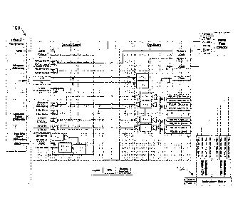
Preliminarily, the top level block diagram in FIG. 3 depicts an exemplary
RPA module 100 dual-board PCB/PWB design consisting of a first (in an
exemplary embodiment, a bottom) board 101, which incorporates the high-level
field director and Inductosyn drive signals, and a second (in an exemplary
embodiment, a top) board 102, which reads and amplifies the small amplitude
Inductosyn output signals. The dual board configuration separates the low
level
9
CA 02985817 2017-11-10
WO 2016/183343 PCT/US2016/032145
sensitive signals from the high level excite signals. The low level sensitive
signals are located on the top board and the excite signals are located on the
bottom board. The separate board configuration provides physical separation
between the boards providing isolation between the circuit functions.
The RPA module interfaces to the field director 103 and lnductosyn 104
located at each arm joint. The RPA module contains three signal paths. The
first
signal path includes circuitry that drives the field director and lnductosyn
primaries. The circuit receives a differential signal from the robotic control
electronics, conditions it, and then amplifies this signal in order to drive
the field
director and Inductosyn primaries. The second signal path amplifies the sine
(Sin) and cosine (Cos) outputs from the field director secondary, conditions
those signals, and converts them to a differential output. This signal is then
output to the control electronics. The last signal path amplifies the sine and
cosine outputs from the lnductosyn secondary, conditions those signals, and
converts them to a differential output. These signals are also output to the
control electronics.
The excite drive circuit 110, schematically represented in FIG. 4, includes
a differential line receiver, a phase adjustment circuit, and a power output
stage
to drive the Inductosyn rotor (primary).
The input circuit consists of operational amplifier 111, which converts the
differential input signal to a single ended output. The input circuit contains
differential and common-mode filtering to limit the input signal bandwidth and
reduce noise. The gain of the circuit is less than one since, in this
application,
the input signal is large. The output of 111 feeds a phase shift circuit 112
consisting of op-amp 113 and its associated components. This circuit can be
configured to add phase lead or lag to the excite drive signal. The phase
adjustment can be used to ensure the phase alignment of the reference and
recovered signals at the resolver-to-digital converter. Including the phase
shift
circuit within the excite drive amplifier allows individual phase adjustment
when
multiple resolvers are used in a system. The phase shift circuit drives an
output
stage that provides current drive to the resolver primary. The driver stage is
enclosed within a feedback loop to set the operating point and reduce signal
distortion. The driver circuit is current limited and can operate from 400 Hz
to 25
CA 02985817 2017-11-10
WO 2016/183343 PCT/US2016/032145
kHz. The driver contains filter components that reduce the excite drive signal
coupling into the power rails. The series current limiting resistor 114 is
chosen to
limit the drive current to the appropriate level for the Inductosyn unit
selected.
The outputs of the Inductosyn stator (secondary) are fed to the recovery
amplifiers 120 to bring the low level signals to line levels. The recovery
amplifiers
120, schematically shown in FIG. 5, provide very high gain (3000-5000) to
amplify the recovered Sin and Cos signals to a level where they can be
processed by the resolver-to-digital converter. The recovery amplifier chain
includes three amplifier stages and a unity gain differential line drive
circuit. The
line driver circuit drives the amplified signals through interconnecting
cables to
the resolver-to-digital converter electronics.
The first gain stage includes of a 10:1 input transformer to provide
galvanic isolation and increase the signal-to-noise ratio. The transformer 121
provides high common-mode rejection and RF filtering, reducing the coupling of
anomalous signals into the amplifier chain. The transformer 121 and the first
op
amp gain stage 122 set the overall signal-to-noise ratio of the amplifier
chain.
Since the amplifier gain is very high, a low noise floor ensures an adequate
signal-to-noise ratio. The transformer has a low primary resistance to
minimize
Johnson noise (electronic noise generated by thermal agitation of charge
carriers inside an electrical conductor at equilibrium, which happens
regardless
of any applied voltage) and is housed in a magnetic shield to minimize stray
signal pickup.
The transformer secondary is connected to op-amp 123, a non-inverting
low noise gain stage. A low pass filter is provided at the input to the op-amp
to
roll off noise above 25 kHz. Op-amp 123 can be set to provide between 20 dB
and 50 dB by selection of the feedback components. The stage is configured as
an AC amplifier with the gain dropping to unity at DC. This configuration
minimizes the DC offset at the output of the amplifier to improve dynamic
range.
The output of this stage is coupled to a band pass filter that attenuates the
noise
level by 6 dB. The filter bandwidth is wide to ensure a flat gain and phase
response at the carrier operating frequency. The next stage consists of an
inverting amplifier 125 that provides the final amplification stage. The gain
can
be set to provide between 20 dB and 50 dB by selection of the feedback
11
CA 02985817 2017-11-10
WO 2016/183343 PCT/US2016/032145
components. The output of this stage is AC coupled to the differential cable
driver stage so that any DC offsets that may be present are blocked from
reaching the line driver stage.
The line driver circuit 130, schematically shown in FIG. 6, includes
inverting and non-inverting unity gain amplifiers that provide a differential
signal
output to interface with the resolver-to-digital converter receivers and
interconnecting cables. The driver design provides a low output impedance
while
isolating the driver from the cable capacitance to ensure stability. The low
output
impedance ensures high common-mode rejection at the receiver. To provide low
output impedance and isolation from the interconnecting cable capacitance, the
circuit provides two feedback paths. DC feedback is taken from the outside of
the isolation resistor lowering the output impedance. AC feedback is taken
directly at the op-amp output ensuring high frequency stability. Phase
compensation is also provided to compensate for the bandwidth differences
between the inverting and non-inverting op-amp configuration used in the
driver
circuit. The compensation ensures that the differential output signals are
exactly
180 degrees out of phase.
The outputs of the field director are fed to a combined amplifier line driver
circuit 140, shown in FIG. 7, that amplifies the Sin and Cos signals to a
level
where they can be processed by the resolver-to-digital converter. In this
application the outputs of the field director are high-level signals so a low
gain
circuit is used. The circuit is AC coupled, which minimizes the DC offset at
the
output of the amplifier. As with the driver circuit for the Inductosyn
amplifiers, the
driver design provides low output impedance while isolating the driver from
the
cable capacitance to ensure stability and uses the same dual-feedback
technique previously described.
Referring now to FIGs. 8 and 9, the exemplary module includes extensive
power supply decoupling to keep noise on the power rails from feeding into the
recovery amplifier chain. Capacitors 151, 152 on the input power rails provide
the first stage of filtering for the design. For the sensitive low-noise
circuitry, a
two-stage filter topology is used. A bulk RC filter 153 provides a second
stage of
filtering for all the high gain amplifier stages, and an individual RC filter
is
provided for each op amp in the amplifier chain. Additionally, the excite
drive
12
CA 02985817 2017-11-10
WO 2016/183343 PCT/US2016/032145
circuit 110 includes filters to keep the drive signal that drives the
Inductosyn from
modulating the power rails.
Referring now to FIG. 10, in exemplary embodiments the Printed Circuit
Board (PCB) is designed with multiple layers to shield and isolate signals.
Circuit
functions and routing are arranged to provide minimal signal coupling with
adjacent circuits. Individual layers include isolated ground planes and guard
rings to isolate sensitive circuitry. Grounding is a significant performance
issue.
As such, the low level signals come into the PCB through the connector on the
left side. The Inductosyn 127x and 128x SIN and COS signals are treated as
separate analog channels (channel 1-4). Each channel goes to a different pre-
amp purposely separated in segmented "islands" denoted by the letters A-D. In
addition, the underlying ground planes are segmented according to the channel
input circuitry to prevent inner channel currents from coupling with one
another.
Referring now to FIG. 11, the input signal path is routed in a sub-layer
surrounded by segmented ground planes 170 to further reduce noise coupling.
After the pre-amp, the segmented ground planes are again joined as one analog
ground plane in a star ground.
Even with exemplary Compact RPA Module's compact dual-board design,
the ability to provide signal-to-noise isolation and reduction of crosstalk
between
the signals flowing on the PCBs is retained. This allows the RPA module to
provide accurate absolute joint position telemetry to the robotic arm control
electronics to support high-fidelity knowledge of robotic arm joint position
during
robotic operations. Exemplary embodiments support Inductosyns being used in
applications where, previously, reliable operation has been problematic due to
the limitations of conventional systems, especially for applications requiring
small
form factors.
Turning now to FIGs. 12-29, shown are various exemplary layer
specifications for an exemplary top board. In particular, FIG. 12 shows a top
view of an exemplary RPA module top board assembly. FIG. 13 shows a bottom
view of an exemplary RPA module top board assembly. FIG. 14 shows the
component side of layer 1 of an exemplary RPA module top board. FIG. 15
shows a ground plane (layer 2) of an exemplary RPA module top board. FIG. 16
shows an inner signal layer (layer 3) of an exemplary RPA module top board.
13
CA 02985817 2017-11-10
WO 2016/183343 PCT/US2016/032145
FIG. 17 shows a ground plane (layer 4) of an exemplary RPA module top board.
FIG. 18 shows a power plane (layer 5) of an exemplary RPA module top board.
FIG. 19 shows a power plane (layer 6) of an exemplary RPA module top board.
FIG. 20 shows a power plane (layer 7) of an exemplary RPA module top board.
FIG. 21 shows a power plane (layer 8) of an exemplary RPA module top board.
FIG. 22 shows a ground plane (layer 9) of an exemplary RPA module top board.
FIG. 23 shows an inner signal layer (layer 10) of an exemplary RPA module top
board. FIG. 24 shows a ground plane (layer 11) of an exemplary RPA module
top board. FIG. 25 shows a solder side (layer 12) of an exemplary RPA module
top board. FIG. 26 shows the top solder mask of an exemplary RPA module top
board. FIG. 27 shows the bottom solder mask of an exemplary RPA module top
board. FIG. 28 shows the top silk screen of an exemplary RPA module top
board. FIG. 29 shows the bottom silk screen of an exemplary RPA module top
board.
Turning now to FIGs. 30-47, shown are various exemplary layer
specifications for an exemplary bottom board. FIG. 30 shows a top view of an
exemplary RPA module bottom board assembly. FIG. 31 shows a bottom view of
an exemplary RPA module bottom board assembly. FIG. 32 shows the
component side (layer 1) of an exemplary RPA module bottom board. FIG. 33
shows a ground plane (layer 2) of an exemplary RPA module bottom board. FIG.
34 shows an inner signal layer (layer 3) of an exemplary RPA module bottom
board. FIG. 35 shows a ground plane (layer 4) of an exemplary RPA module
bottom board. FIG. 36 shows a power plane (layer 5) of an exemplary RPA
module bottom board. FIG. 37 shows a power plane (layer 6) of an exemplary
RPA module bottom board. FIG. 38 shows a power plane (layer 7) of an
exemplary RPA module bottom board. FIG. 39 shows a power plane (layer 8) of
an exemplary RPA module bottom board. FIG. 40 shows a ground plane (layer
9) of an exemplary RPA module bottom board. FIG. 41 shows an inner signal
layer (layer 10) of an exemplary RPA module bottom board. FIG. 42 shows a
ground plane layer (layer 11) of an exemplary RPA module bottom board. FIG.
43 shows the bottom solder side (layer 12) of an exemplary RPA module bottom
board. FIG. 44 shows the top solder mask of an exemplary RPA module bottom
board. FIG. 45 shows the bottom solder mask of an exemplary RPA module
14
CA 02985817 2017-11-10
WO 2016/183343 PCT/US2016/032145
bottom board. FIG. 46 shows the top silk screen of an exemplary RPA module
bottom board. FIG. 47 shows the bottom silk screen of an exemplary RPA
module bottom board.
The top board gain structure implements three gain stages per channel to
minimize interaction between the amplifiers. The PWB configuration is unique
in
this application due to the level of complexity used to maintain segregation/
isolation between corresponding lx and 128x channels, segregation of
associated power and ground planes for each channel, and additional ground
shield layers above and below the signal layers implemented within the PWB
stack up. PWB stack up distances/tolerances between layers and locations of
each layer maintain the noise isolation/rejection. Further isolation is
achieved
within the PWB by maintaining all COS signal, power, and ground traces and
planes on the top 6 layers of the board and all SIN signal, power and ground
traces/planes to the bottom 6 layers of the board.
The overall PWB stack up showing the layer stack up dimensions and
tolerances is shown in Figure 48. The stack up and distances between the
layers is arranged to provide signal separation and isolation as described
below.
PWB layers 2, 3, and 4 form the isolation stack up for the sensitive 1X
COS and 128X COS signal amplifiers. The COS sensitive signals are routed on
layer 3 and are located between specific segmented ground planes on layers 2
and 4. These ground planes provide electromagnetic shielding for the sensitive
signals on layer 3. See FIGs. 15-17.
Referring specifically to FIG. 15, (layer 2), the configuration includes a
segmented ground plane having first and second portions 210, 212 for the COS
amplifier channels, 1X COS, and 128X COS, respectively. This plane provides a
top shield layer for the sensitive signals on layer 3, shown in FIG. 16.
Referring now to FIG. 16, layer 3 is shown and is the signal layer. This
layer routes the sensitive 1X and 128X COS signals. These signals are enclosed
by guard rings 310, 312 to shield the sensitive input COS signals prior to the
transformers. The 1X COS signal is enclosed by guard ring 312 and the 128X
COS signal is enclosed by guard ring 310.
Referring now to FIG. 17, layer 4 is shown, and depicts the bottom
segmented ground plane, 410, 412 for the COS amplifier channels 1X COS and
CA 02985817 2017-11-10
WO 2016/183343
PCT/US2016/032145
128X COS, respectively. This plane provides a bottom shield layer for the
sensitive signals on layer 3.
Board layers 5, 6, 7, and 8 (shown in FIGs. 18-21, respectively) form
stack up that provides isolated power to each of the amplifier channels.
Referring now to FIG. 18, layer 5, a power layer is shown. This layer
provides +15V filtered power to the 1X and 128 X COS amplifiers. The power
planes are separated between the 1X and 128X COS channels and are
connected at one point to prevent noise from flowing between adjacent
circuits.
Referring now to FIG. 19, layer 6, a power layer is shown. This layer
provides -15V filtered power to the 1X and 128 X COS amplifiers. The power
planes are separated between the 1X and 128X COS channels and are
connected at one point to prevent noise from flowing between adjacent
circuits.
Referring now to FIG. 20, layer 7, a power layer is shown. This layer
provides -15V filtered power to the 1X and 128 X SIN amplifiers. The power
planes are separated between the 1X and 128X SIN channels and are
connected at one point to prevent noise from flowing between adjacent circuits
Referring now to FIG. 21, layer 8, a power layer is shown. This layer
provides +15V filtered power to the 1X and 128 X SIN amplifiers. The power
planes are separated between the 1X and 128X SIN channels and are
connected at one point to prevent noise from flowing between adjacent
circuits.
Similar to layers 2, 3, and 4, board layers 9, 10, and 11 form the isolation
stack up for the sensitive 1X SIN and 128X SIN signal amplifiers. The SIN
sensitive signals are routed on layer 10 and are located between specific
segmented ground planes on layers 9 and 11. These ground planes provide
critical electromagnetic shielding for the sensitive signals on layer 10. See
FIGs.
22-24
Referring now to FIG. 22, ground layer 9 is shown. The configuration of
this layer utilizes a segmented ground plane 510, 512 for the SIN amplifier
channels 1X SIN and 128X SIN, respectively. This plane provides a top shield
layer for the sensitive signals on layer 10.
Referring now to FIG. 23, signal layer 10 is shown. This layer routes the
sensitive 1X and 128X SIN signals. These signals are enclosed by critical
guard
rings 610, 612 to shield the sensitive input SIN signals prior to the
transformers.
16
CA 02985817 2017-11-10
WO 2016/183343 PCT/US2016/032145
The 1X SIN signal is enclosed by guard ring 612 and the 128X SIN signal is
enclosed by guard ring 610.
Referring now to FIG. 24, ground layer 11 is shown. This layer includes
the bottom segmented ground plane 710, 712 for the SIN amplifier channels, 1X
SIN and 128X SIN, respectively. This plane provides a bottom shield layer for
the sensitive signals on layer 10.
Although the invention has been shown and described with respect to a
certain embodiment or embodiments, it is obvious that equivalent alterations
and
modifications will occur to others skilled in the art upon the reading and
understanding of this specification and the annexed drawings. In particular
regard to the various functions performed by the above described elements
(components, assemblies, devices, compositions, etc.), the terms (including a
reference to a "means") used to describe such elements are intended to
correspond, unless otherwise indicated, to any element which performs the
specified function of the described element (i.e., that is functionally
equivalent),
even though not structurally equivalent to the disclosed structure which
performs
the function in the herein illustrated exemplary embodiment or embodiments of
the invention. In addition, while a particular feature of the invention may
have
been described above with respect to only one or more of several illustrated
embodiments, such feature may be combined with one or more other features of
the other embodiments, as may be desired and advantageous for any given or
particular application.
17