Note: Descriptions are shown in the official language in which they were submitted.
CA 02985852 2017-11-14
WO 2017/024384
PCT/CA2016/050887
PATCH ANTENNA WITH PERIPHERAL PARASITIC MONOPOLE
CIRCULAR ARRAYS
BACKGROUND OF THE INVENTION
Patch antennas are often considered for use in high-performance GNSS multi-
band
antennas due to their planar configuration and easy integration with circuit
boards. Patch
antennas have a number of noted disadvantages, including, e.g., narrow
bandwidth and
high directivity. As patch antennas are based on planar resonators, they
typically operate
best at one certain frequency_ Though several technologies have been used to
increase the
bandwidth available to patch antennas, it is still difficult to achieve
required bandwidth.
This is especially true when the substrate material and given physical size is
limited. The
patch antenna needs a certain size (typically half guided wavelength) to
resonate at the
operation frequency, therefore the beam-width, and consequently the radiation
pattern roll-
off, is often fixed using given material and technology.
SUMMARY OF THE INVENTION
The disadvantages of the prior art are overcome by providing a patch antenna
with
peripheral parasitic monopole circular arrays. The antenna illustratively
comprises of three
elements. A first element comprises of a patch antenna. The patch antenna may
comprise a
single layer or a stacked-layer patch antenna. The second element comprises a
set of
reactive/resistive loaded inonopolcs that are rotational symmetrically
surrounding the
patch antenna. The monopoles may be terminated by certain phase-delay lines.
The third
element comprises a ground plane.
BRIEF DESCRIPTION OF THE DRAWINGS
The above and further advantages are described in reference to the following
figures, in which like reference numerals indicate identical or functionally
similar
elements:
Fig. 1 is a perspective view of an exemplary antenna in accordance with an
illustrative embodiment of the present invention;
Fig, 2A is a top perspective view of an exemplary antenna in accordance with
an
illustrative embodiment of the present invention;
CA 02985852 2017-11-14
WO 2017/024384
PCT/CA2016/050887
Fig. 2B is a side perspective view of an exemplary antenna in accordance with
an
illustrative embodiment of the present invention;
Fig. 3 is a view of propagation of a TM surface wave along a metal/air surface
in
accordance with an illustrative embodiment of the present invention;
Fig. 4 is a view illustrating the interaction of a patch antenna excited
surface wave
with the antenna in accordance with an illustrative embodiment of the present
invention;
Fig. 5A is a perspective view of a patch antenna surrounded by vertical wire
monopoles in accordance with an illustrative embodiment of the present
invention;
Fig. 5B is a perspective view of a patch antenna surrounded by inverted L
monopoles in accordance with an illustrative embodiment of the present
invention;
Fig. 5C is a perspective view of a patch antenna surrounded by printed strip
inverted L spiral monopoles in accordance with an illustrative embodiment for
the present
invention;
Fig. 5D is a perspective view of a patch antenna surrounded by a multi-array
of
inverted L spiral monopoles in accordance with an illustrative embodiment of
the present
invention;
Fig. 6 is a graph illustrating the active return loss of an antenna in
accordance with
an illustrative embodiment of the present invention;
Fig. 7 is a set of graphs illustrating radiation patterns in accordance with
an
illustrative embodiment of the present invention;
Fig. SA is a view of an alternative radiation pattern in accordance with an
illustrative embodiment of the present invention:,
Fig. 8B is a view of an alternative radiation pattern in accordance with an
illustrative embodiment of the present invention; and
75 Fig. SC is a view of an alternative radiation pattern in accordance
with an
illustrative embodiment of the present invention.
DETAILED DESCRIPTION OF AN ILLUSTRATIVE EMBODIMENT
A patch antenna constructed in accordance with illustrative embodiments of the
present invention utilizes a pin-wheel shaped surrounding monopole radiators
to excite the
surface wave excited by the patches. Such an antenna has several advantages
over the
prior art. First, an antenna made in accordance with principles of the present
disclosure
has a much improved bandwidth due to the coupling of the multiple surround
monopole
CA 02985852 2017-11-14
WO 2017/024384
PCT/CA2016/050887
3
radiators. Second, a patch antenna in accordance with the principles of the
present
disclosure provides a reduced cross-polarization due to the surface wave
current
manipulation. Further, the circular polarization is improved by using multiple
feeds and
sequential rotationally excited spiral pin-wheel shaped surrounding radiators.
Third, an
antenna in accordance with the present disclosure provides beam shaping
capability in that
the position, shape and refractive coefficients of the surrounding radiators
may be varied
to change the radiation pattern.
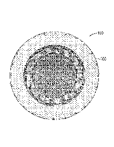
Fig. 1 is a perspective view 100 of an exemplary antenna 105 in accordance
with
an illustrative embodiment of the present invention. View 100 shows in
overview, the
various elements of the patch antenna in accordance with an illustrative
embodiment. Fig.
2A is a top perspective view 200A of the antenna 105 illustrating the various
elements in
more details in accordance with an illustrative embodiment of the present
invention. The
antenna 105 illustratively comprises a ground plane 205 over which one or more
patch
antennas 220 arc overlaid. One or more feed points 225 are operatively
connected to the
patch antennas 220. A plurality of monopoles 210 are arranged around the patch
antennas
220. In certain illustrative embodiments, the monopoles may be terminated with
phase
delay lines 215.
Fig. 2B is a side perspective view 200B of an exemplary antenna in accordance
with an illustrative embodiment of the present invention. As can be seen, the
one or more
patch antennas 220 may be arranged in a stacked configuration. Three patch
antennas are
shown; however, it should be noted that in alternative embodiments, any number
may be
utilized. Thus, the description and illustration of three antennas 220 should
be taken as
exemplary only.
A patch antenna equivalently radiates at the resonant slot ring formed between
the
metallic patch and the ground plane. Since the dielectric substrate for
antennas typically
has a truncated edge, it does not support the propagation of dielectric/metal
interface
bounded surface waves. However, the fringe field in the patch edge does launch
TM
surface waves propagating along the air-metal (ground plane) surface. Fig. 3
is an
illustration 300 of the propagation of TM surface waves along the metal/air
surface. Such
a surface wave is also called surface plasmons in optics, and at microwave
frequency it
extends a great distance into the surrounding space with very low decaying
factor. The H-
fields of such a wave are transverse to the direction of the propagation,
wherein
corresponding longitudinal surface current flows on the metal conductor; while
the E-
CA 02985852 2017-11-14
WO 2017/024384
PCT/CA2016/050887
4
fields are linked to oscillating (at the frequency of the radiating waves)
charges distributed
on top of the metal and therefore forming loops vertically jumping in and out
of the
surface along the longitude direction. It propagates at nearly the freespacc
speed of the
light. It is therefore often described as surface currents, rather than
surface waves in
microwave and in fact they are not so different than the normal alternating
currents on any
conductor.
The surface wave travels from the formed patch-slot ring all the way to the
edge of
the truncated ground plane, then would be diffracted, where it re-radiates to
the space as if
the metal edge were point sources. These radiations contribute to the far-
field of the
antenna in all direction, the upper-hemisphere, lower-hemisphere and the
horizon. For
GNSS applications, these unexpected radiations generally increase the
reception of noise
signal from multipath or nearby interferences. Several technologies have been
used to
suppress or attenuate the TM surface current from propagating, such as chock
ring and
resistive stealth ground plane. The surface impedance for the wave on a flat
metal sheet is
derived as
ff,
- - 1+j [12 Di. (1)
where a is the metal conductivity, 6 is the skin depth. From this equation, a
conductor
surface typically shows low surface impedance.
Fig. 4 is an illustration 400 of the interactions of the patch antenna excited
surface
wave with the antenna in accordance with an illustrative embodiment of the
present
invention. Illustratively, surface wave is generated by the patch antenna and
then it travels
and hits on the surrounding monopole elements before it reaches the edge of
the ground.
Depending on the loading impedance of the RLC tank (Z1 RIIIIIC it is a
combination of R, L and C, which can be designed to control its matching to
the input
impedance of the monopole at the port), some part of the surface wave signals
induced in
the parasitic monopoles are first guided through the phase-delay lines and
then are
reflected (scattered) and re-radiated. The reflection coefficient at the
monopole is
r _ (2)
zo-zo (RL-Fzu)2 ¨xL
,
where Z0 is the characteristic impedance of the delay line. If the load is
resistive (with R
only in the loading tank, X1=0), some part of the surface wave power is
attenuated:
CA 02985852 2017-11-14
WO 2017/024384
PCT/CA2016/050887
RL-zo
r = (3)
RL-Fzo
In the case of a short-circuited (Z4=0), total reflection happens at the
monopole port and
the monopole "captured- power is completely re-radiated:
-zo
(4)
zo
5 If the load is lossless (R1=0) and reactive, the reflection coefficient
reads:
r = ________________________________ = 1 +j ___ , (5)
1-xL
where. is the normalized reactance of the terminating load to Zo. From this
=
z,
equation we know that the phase of the reflected signal is controllable by
varying the
reactance value and length of the delay line:
10_ 25z-L
= tan (6)
-1
The equation (6) reveals two points. First, the phase of the re-radiated
signal from each
monopole can be varied by tuning the reactance load. Second, when the load
reactance is
small, the phase has more significant change compared to very large reactance.
The magnitude of the re-radiated power will also depend on structure of the
monopoles, for instance, the height and shape of the monopole defines how much
power is
induced and also the radiation efficiency. Typically, the parasitic elements
are near to
resonance to re-radiate the surface wave more efficiently, i.e., when the
total length of the
monopole is close to multiple-quarter of guided wavelength, the system reaches
highest
efficiency.
Assuming the excitation current of center patch is hi and the corresponding
radiated far field is K.: and the peripheral N monopoles are equally spaced
along a ring,
from circular antenna array theory the total radiated electric field is
written as the
superposition of the contributed fields from all the radiators
'kd E=ri CO2.
E 9, = E,(r. 0.0) - e- 3
(7)
CA 02985852 2017-11-14
WO 2017/024384
PCT/CA2016/050887
6
where k is the freespace wavenumber, k, is the surface-wave wavenumber (k, k),
d is the
distance from center patch to the surrounding monopole ring (the radius of the
ring), ris
the reflection coefficient at parasitic monopole n, and represents the
field radiated
by a single monopole element Ili. By varying the distance between the patch to
the
surrounding monopoles and the reflection coefficient (magnitude and phase),
certain type
of radiation pattern could be synthesized. Based on this principle, single-fed
reactively
beam- or null-steered antennas are possible.
This concept maybe explained in analogy to reflect-array where an array of
reactively-terminated antenna elements is placed at the reflector position
facing a source
exciter to achieve very high-gain or stcerable beam antenna array. In current
proposal, the
source is the surface wave generated by the antenna, and the reflector array
is located in
the same plane as the source. In another way, this monopole structure can also
be
explained as high-impedance surface (the impedance is much higher than the
surface wave
impedance) that scatters the surface wave to the space.
Due to this process, the surrounding parasitic monopoles act as the loads to
the
main patch antenna which reduces the quality (0) factor of the patch
resonators. This
results in a substantial increase in the bandwidth of the antenna. Further,
this process
causes the near field and far field of the antenna to be changes, therefore
the radiation
pattern of the antenna can be varied. An example of this varying is that the
roll-off may be
decreased or increased. As will be appreciated by those skilled in the art,
this is
sometimes desirable for GNSS applications. Additionally, the axial ratio at
the low-
elevation angle may be improved since the unwanted diffraction at the ground
edge is
manipulated by the purposely added parasitic radiators.
Figs. 5A-5D illustrate various alternative embodiments of the present
invention.
Exemplary view 500A (Fig. 5A) is of a patch antenna 220 surrounded by vertical
wire
monopoles 210. The monopoles may, in alternative embodiments, be connected to
phase
delay lines 215. View 500B (fig. 5B) is of an alternative embodiment where the
monopoles 210 are in the shape of inverted L's. Fig. 5C is a top perspective
of an
alternative embodiment where the patch antenna is surrounded by printed strip
inverted L
spiral monopoles. Fig. 5D is a tope perspective view 500D of the patch antenna
surrounded by a multi-array of inverted L monopoles. As will be appreciated by
Figs. 5A-
5D, a wide variety of arrangements of the monopoles may be utilized in
accordance with
CA 02985852 2017-11-14
WO 2017/024384
PCT/CA2016/050887
7
alternative embodiments of the present invention. Thus, the present invention
should not
be viewed as limited to those specific examples described herein.
Depending on the required radiation performance, the surrounding monopoles may
take the shape of vertical wires, inverted-L (or inverted-F), and printed
inverted-L spirals
(which forms a pin-wheel shape). Besides this, one, two or more surrounding
arrays of
monopoles with different lengths may be combined to provide more flexibility
for forming
the beam according to the total radiation given in Eq.7: more arrays may
provide more
frequencies of operation; different clock-wise orientation of the spirals may
give control of
different polarization; and the interactions among the neighboring arrays may
show more
exotic electromagnetic band-gap effect which is useful for multipath
rejections.
The present invention utilizes a patch antenna system with increased
bandwidth,
improved radiation pattern and reduced rolling-off for GNSS application. By
varying
loading circuit, the radiation pattern may be controlled. The antenna only
needs to be fed
at the center patch antenna clement with multiple quadrature feeds. The design
has a
number of advantages, including, e.g., increased bandwidth, reduced cross
polarization,
varied radiation patterns and low cost.
Fig. 6 is a chart 600 that compares the active return loss of a quad-fed
stacked GNSS
patch antennas with and without a single-array of pin-wheel spiral shaped
parasitic
peripheral monopoles in accordance with embodiments of the present invention.
Chart 600
shows that the impedance bandwidth of the antenna is improved significantly,
which is
favored in most situations. It should be noted that utilizing a single array
of pin-wheel
spiral shaped parasitic peripheral monopoles should be taken as an exemplary
embodiment
only.
Fig, 7 is a chart 700 that compares the polar radiation patterns for one of
the new
antenna with the one without the parasitic pin-wheel monopoles. The axial
ratio is
decreased by using the proposed structure and the low-elevation angle multi-
path could be
improved too. Additional study has shown that using resistive loading, or
adding some
specially designed monopole patterns, the front-to-back ratio is significantly
increased.
It is demonstrated from above realized-gain radiation pattern comparisons, the
horizon
(0=90') right-handed circular polarization gain is improved by 2.2dB for L I
(1575.4
MHz) frequency, and 2.6 dB for L2 (1227.6 MHz) frequency.
CA 02985852 2017-11-14
WO 2017/024384
PCT/CA2016/050887
8
It should be noted that the results described herein are demonstrated as an
example
only, and the radiation patterns can be manipulated by certain design
according to system
requirements, especially by using multi-array of parasitic elements and/or
using different
loading circuits. For example, Fig. 8A shows an achieved RHCP radiation
pattern with
higher directivity (9.4 dBic gain at zenith, and quickly roll down by 17.4 dB
to ¨8 dBic at
horizon) and low back-side cross-polarization radiation. Fig. 8B is an another
example that
illustrates that the RI-ICI) radiation shows a near conical pattern, 0.2 dBic
low at zenith
while as high as ¨0.5 dBic at horizon, which is ideal for low-elevation
coverage. A third
example is shown in Fig. 8C in which the RHCP radiation pattern is almost
omnidirectional in the upper-hemisphere, for which the gain roll-off from
zenith to
horizon is only about 5 dB.
The parasitic antenna elements may be printed as simple traces at the same
layer as
one or several of the patches. It is easily to be integrated with the passive
or active loading
circuit with tuning or switching capability.
I 5 While various embodiments have been described herein, it should be
noted that the
principles of the present invention may be utilized with numerous variations
while keeping
with the spirit and scope of the disclosure. Thus, the examples should not be
viewed as
limited but should be taken as way of example.