Note: Descriptions are shown in the official language in which they were submitted.
CA 02986370 2017-11-17
WO 2016/189510 PCT/IB2016/053137
1
IMAGING DEVICE
FIELD
The present disclosure relates to an imaging device for projecting a plurality
of
individually controllable laser beams onto a surface that is movable relative
to the imaging
device. The imaging device will be described herein mainly by reference to its
application in
digital printing systems but its use is not limited to this application.
BACKGROUND
US 7,002,613 describes a digital printing system to which the imaging device
of the
present disclosure is applicable. In particular, in Figure 8 of the latter
patent specification,
there is shown an imaging device designated 84 that is believed to represent
the closest prior
art to the present disclosure. The imaging device serves to project a
plurality of individually
controllable laser beams onto a surface, herein termed an imaging surface, to
generate an
energy image onto that surface. The laser image can be used for a variety of
purposes, just a
few examples being to produce a two dimensional printed image on a substrate,
as taught for
instance in US 7,002,613, in 3D printing and in etching of an image onto any
surface.
For high throughput applications, such as commercial printing or 3D
lithography, the
number of pixels to be imaged every second is very high, demanding parallelism
in the
imaging device. The laser imaging device of the present disclosure is intended
for
applications that require energy beams of high power. One cannot therefore
merely scan the
imaging surface with a single laser beam, so as to expose the pixels
sequentially. Instead, the
imaging device is required to have a separate laser emitting element for each
pixel (picture
element) of the image area of the imaging surface.
To achieve acceptable print quality, it is important to have as high a pixel
density as
possible. A high resolution image, for example one having 1200 dpi (dots per
inch), requires a
density of laser emitting elements that is not achievable if the laser
emitting elements all lie in
a straight line, due to the amount of overlap necessary between the laser
sources to achieve a
uniform printing quality. Aside from the fact that it is not physically
possible to achieve such
a high packing density, adjacent elements would interfere thermally with one
another.
Semiconductor chips are known that emit beams of laser light in an array of M
rows and
N columns. In US 7,002,613 the rows and columns are exactly perpendicular to
each other but
the chips are mounted askew, in the manner shown in Figure 1 of the latter
patent, so that
CA 02986370 2017-11-17
WO 2016/189510 PCT/IB2016/053137
2
each row can fill in the missing pixels of the preceding row(s). In this way,
such an array can
achieve a high resolution image but only over the width of the chip and such
chips cannot
simply be mounted side by side if one is to achieve a printed image without
stripes along its
length, because the chips cannot have laser emitting elements positioned
sufficiently close to
their lateral edges.
US 7,002,613 avoids this problem by arranging such chips in two rows, in the
manner
shown in Figure 8 of the latter patent. The chips in each row are staggered
relative to the chips
in the other row of the pair so that each chip in one row scans the gap left
unscanned by the
two adjacent chips in the other row.
Even though it is expected that the rows of chips will be mounted on a support
under
clean laboratory conditions using a microscope to achieve their correct
alignment, it is not
possible to guarantee that the relative alignment of the chips in the two rows
will be accurate
within the resolution of the printed image. Any misalignment will result in
the image having
stripes or other undesired defects.
US 2010/080594 and US 2008/181667 describe systems in which the light from
arrays
of LED's (rather than laser sources) is projected onto an image surface and
teach how steps
may be taken to compensate for any misalignment between the arrays. In each
case, the
images produced by adjacent arrays are overlapped and selected LED's from one
or other of
the two arrays are activated to maintain image continuity at the boundary
between the two
arrays. In the case of US 2010/080594 this overlap is shown clearly in Figure
14 and in US
2009/181667 it is evident, for example, from Figures 9A and 9B.
SUMMARY
In the present disclosure, there is proposed an imaging device for projecting
individually controllable laser beams onto an imaging surface that is movable
relative thereto
in a reference X-direction, the device including a plurality of semiconductor
chips each of
which comprises a plurality of individually controllable laser beam emitting
elements
arranged in a two dimensional main array of M rows and N columns, the elements
in each
row having a uniform spacing (A) and the elements in each column having a
uniform spacing
(a,), wherein the chips are mounted on a support in such a manner that each
pair of chips that
are adjacent one another in a reference Y-direction, transverse to the X-
direction, are offset
from one another in the X-direction, and, when activated continuously, the
emitted laser
beams of the two chips of said pair trace on the imaging surface 2-M=N
parallel lines that
CA 02986370 2017-11-17
WO 2016/189510 PCT/IB2016/053137
3
extend in the X-direction and are substantially uniformly spaced in the Y-
direction, the laser
beams of each chip tracing a set of M=N lines that do not overlap the set of
lines of the other
chip, wherein in addition to the M rows and N columns of elements of the main
array, each
chip comprises at least one additional column on each side of the main array,
each containing
at least one selectively operable laser emitting element capable of
compensating for any
misalignment in the Y-direction in the relative positioning of the adjacent
chips on the support
by tracing at least one additional line that lies between the two sets of M=N
lines.
Assuming that the M rows and N columns of laser emitting elements of the main
array
do not include any elements that are normally redundant, the spacing between
adjacent lines
in the set will be equal to Ar/M, namely the spacing of the adjacent elements
in each row
divided by the number of rows. Furthermore, because in the present disclosure
there is no
overlap between the two sets of 1\71=N lines traced by any two adjacent chips,
the total number
of lines traced by the two chips will be equal to 2-M=N, namely twice the
product of the
number of rows and the number of columns in each chip, if the chips have equal
numbers of
rows and columns.
In the present proposal, in addition to these evenly spaced lines produced by
the main
arrays, additional laser emitting elements are provided at both ends of each
array intended
only to compensate for chip misalignment. If adjacent chips are correctly
aligned, the
elements of the additional columns will be redundant and will not be
energized. However, if a
gap should remain between the lines traced by adjacent chips, the additional
elements can
introduce additional lines to fill that gap at a position approximating to the
uniform spacing of
the lines traced by the main arrays It should be noted that, in contrast to
the proposals in US
2010/080594 and US 2008/181667, the lines traced by the additional elements do
not fall
between (i.e. are not interlaced with) the lines of either set of M=N lines
traced by the main
arrays and only fall within any gap between the two sets of M=N lines.
In the event of an overlap between the two sets of M=N lines traced by the
elements of
adjacent chips, some of the elements of the main arrays can be switched off
and if necessary
replaced by an element of the additional columns to maintain the appearance of
a raster with
uniformly spaced lines.
On the other hand, if there is a gap between the two M=N lines traced by the
elements of
adjacent chips, the additional columns can be activated to maintain the
appearance of a raster
with uniformly spaced lines.
CA 02986370 2017-11-17
WO 2016/189510 PCT/1B2016/053137
4
One of the additional elements may be activated on its own if its position
coincides with
a line that would render the raster uniform. Alternatively, if the elements
have a symmetrical
energy profile, resembling for example a Gaussian or a sinusoidal
distribution, it is possible,
by activating both elements to irradiate adjacent spots on the imaging surface
and separately
adjusting the power of each element, to produce a single raster line at an
adjustable distance
from the raster lines of the main elements of the two chips. It should be
noted that this effect
is thermally dynamic and additive provided that the adjacent spots are
irradiated within a
finite time of each other. In other words, the imaging surface should not have
time to dissipate
the energy of the first laser pulse in the interval between the two laser
pulses.
Conveniently, the lines traced by elements in the same additional column are
evenly
spaced from one another, the spacing between the lines traced by the element
of the additional
column being substantially equal to the quotient of the spacing of the lines
traced by the
elements of main array and the number of elements in the additional column.
While it would be possible to use chips in which the rows and columns of the
main
arrays of laser emitting elements are perpendicular to one another, as taught
in US 7,002,613,
this requires the chips to be placed at an angle relative to the Y-direction.
In some
embodiments of the present disclosure the elements in each row of each chip
lie on a line
parallel to the Y-direction and the elements in each column of each chip lie
on a straight line
inclined at an angle to the X-direction. In other words, instead of the
outline of the array being
square, the array is shaped as a parallelogram. This arrangement, which may be
considered
slightly wasteful as far as chip area is concerned, can be advantageous in
terms of assembling
procedure.
It is convenient for the chips to be arranged in at least one pair of rows on
the support,
with corresponding laser emitting elements of all the chips in each of the two
rows lying in
line with one another in the Y-direction. By -corresponding elements" it is
meant that the
individual laser emitting elements should occupy the same row and column
positions within
their respective chips. It is advantageous for corresponding elements in any
group of three
chips in the pair of rows that are adjacent one another in the X and Y-
directions to lie at the
apices of congruent equilateral triangles. This simplifies the construction of
a lens system that
is needed to focus the laser beams onto the imaging surface.
It has been found particularly advantageous for all the laser beams emitted by
one chip
to be focused on the imaging surface by a common single lens, or a common set
of lenses
arranged in series, having a magnification of 1. In other words, the image of
the array of
RECTIFIED SHEET (RULE 91) ISA/EP
CA 02986370 2017-11-17
WO 2016/189510 PCT/IB2016/053137
laser elements on the imaging surface (i.e. an array of dots) should have the
same size as the
array on the chip, though it may be inverted. In such a case even if there is
a slight
misalignment of the lenses, such as GRIN rod (Gradient-Index) lenses, in the
XY plane
perpendicular to the optical axis of the lens, the position of the illuminated
laser spot on the
5 imaging
surface will remain unchanged, as it only depends on the position of the laser
emitting element on the laser array chip. The former elements can be
positioned with very
high accuracy on every laser array chip using standard semiconductor
manufacturing
techniques.
While the lens system may comprise a single GRIN rod associated with each
chip, it
may alternatively comprise a plurality of GRIN rods arranged in series with
one another and
forming a folded light path. In the latter case, a prism common to all the
chips may serve to
direct the laser beams from one GRIN rod element to the next in each series.
In such a folded light path configuration, it is desirable for the prism to be
made of a
glass having a higher refractive index than the GRIN rods.
It is convenient for each chip to have in the main array an equal number of
rows and
columns of laser beam emitting elements (i.e., M = N), as this minimizes the
size of the lens
array.
Within each chip, the separation between the laser elements should be
sufficiently great
to avoid thermal interference between adjacent laser emitting elements.
The support for the chip arrays may be fluid cooled to help dissipate the heat
that may
be generated by the chips.
Furthermore, the support may be a rigid metallic or ceramic structure and it
may be
formed of, or coated with, an electrically insulating surface bearing film
conductors to supply
electrical signals and power to the chips.
The chips in some embodiments are vertical cavity surface emitting laser
(VCSEL) chip
arrays.
In some embodiments, the intensity of the laser beam emitted by each element
may be
adjustable either continuously (in an analogue manner) or in discrete steps
(digitally). In one
embodiment, the chips may include D/A converters so as to receive digital
control signals. In
this way, the laser beam intensity may be adjusted in 4, 8, 16, 32 or up to
4096 discrete steps.
CA 02986370 2017-11-17
WO 2016/189510 PCT/IB2016/053137
6
In a further aspect of the present disclosure, there is provided a method of
projecting
individually controllable laser beams onto an imaging surface that is movable
relative to an
imaging device utilising the imaging device of the present disclosure.
In some embodiments, at least one pair of laser elements, selected either both
from the
same array or one from each of two adjacent arrays, are controlled in such a
manner that their
energies are combined on the imaging surface to increase the temperature of
the imaging
surface above a predetermined threshold at a point intermediate the centers of
the images of
the two laser elements on the imaging surface, without raising the temperature
of the imaging
surface at at least one of the centers of the images of the two laser elements
above the latter
threshold.
BRIEF DESCRIPTION OF THE DRAWINGS
Some embodiments of the imaging device are described herein with reference to
the
accompanying drawings. The description, together with the figures, makes
apparent to a
person having ordinary skill in the art how the teachings of the disclosure
may be practiced,
by way of non-limiting examples. The figures are for the purpose of
illustrative discussion
and no attempt is made to show structural details of an embodiment in more
detail than is
necessary for a fundamental understanding of the disclosure. For the sake of
clarity and
simplicity, some objects depicted in the figures are not to scale
In the Figures:
Figure 1 is a schematic diagram of a digital printing system utilizing an
imaging device
according to an embodiment of the present disclosure;
Figure 2 shows part of an imaging device comprising a set of VCSEL chips
mounted on
a support;
Figure 3 is a schematic representation of the laser emitting elements of two
VCSEL
chips and the lines that they can trace on a relatively moving imaging
surface;
Figure 4 is a schematic representation that demonstrates in one pair of rows
the
alignment between the VCSEL chips and the GRIN rods used as lenses to focus
the emitted
laser beams onto the imaging surface;
Figures 5A shows prior art proposals for correction of chip misalignment;
CA 02986370 2017-11-17
WO 2016/189510 PCT/IB2016/053137
7
Figure 5B shows the manner in which the present disclosure compensates for
chip
misalignment;
Figure 6 shows the energy profiles produced by the laser elements at the ends
of two
adjacent arrays, to illustrate how a single line can be traced using two
laterally positioned
laser elements, there being shown for each array three elements of the main
array and one of
the additional elements;
Figure 7A is a similar energy diagram to Figure 6 to show how the energies of
two
adjacent laser elements of the main array can be combined on the imaging
surface to produce
an additional dot that does not fall on the center line of either of the laser
elements;
Figure 7B shows the dot pattern on the imaging surface produced by activating
four
laser elements of the main array in the manner shown in Figure 7A;
Figure 8A shows how the dot pattern of Figure 7B assists in anti-aliasing;
Figure 8B shows for comparison with Figure 8A the jagged edge that normally
occurs
when printing an oblique line; and
Figure 9 shows an alternative lens system to that shown in Figure 1 that has a
folded
light path to permit more compact packaging in a printing system
DETAILED DESCRIPTION
Overall description of an exemplary printing system
Figure 1 shows a drum 10 having an outer surface 12 that serves as an imaging
surface.
As the drum rotates clockwise, as represented by an arrow, it passes beneath a
coating station
14 where it acquires a monolayer coating of fine particles. After exiting the
coating station 14,
the imaging surface 12 passes beneath an imaging device 15 of the present
disclosure where
selected regions of the imaging surface 12 are exposed to laser radiation
which renders the
particle coating on the selected regions of the surface 12 tacky. Next, the
surface passes
through an impression station 19 where a substrate 20 is compressed between
the drum 10 and
an impression cylinder 22. This causes the selected regions of the coating on
the imaging
surface 12 that have been rendered tacky by exposure to laser radiation by the
imaging device
15 in the correspondingly termed imaging station to transfer from the imaging
surface 12 to
the substrate 20.
CA 02986370 2017-11-17
WO 2016/189510 PCT/IB2016/053137
8
The term "tacky" as used herein is intended to mean that the irradiated
particle coating
is not necessarily tacky to the touch but only that it is softened
sufficiently to be able to
adhere to the surface of a substrate when pressed against it in the impression
station 19.
The regions on the imaging surface 12 corresponding to the selected tacky
areas
transferred to the substrate consequently become exposed, being depleted by
the transfer of
particles. The imaging surface can then complete its cycle by returning to the
coating station
14 where a fresh monolayer particle coating is applied only to the exposed
regions from
which the previously applied particles were transferred to the substrate 20 in
the impression
station 19
In the present proposal, because the particles adhere to the imaging surface
more
strongly than they do to one another, the applied coating of particles, also
interchangeably
termed a particle layer or coating, is substantially a monolayer. While some
overlap may
occur between particles, the layer may be only one particle deep over a major
proportion of
the area of the surface and most, if not all, of the particles will have at
least some direct
contact with the imaging surface. Thus, the average thickness of the monolayer
can be
approximated by the average thickness of the individual particles forming it
or, in some
regions where particles overlap, by a low multiple of the dimension of the
constituting
particles, depending on the type and extent of the overlap. A monolayer may
therefore have a
maximum thickness (T) corresponding to up to about three times a thinnest
dimension
characteristic to the particles involved (e.g., the thickness of the particles
for flake shaped
ones or essentially the particle diameter for spherical ones).
The formation of a substantial monolayer mosaic of particles occurs for the
same reason
that an adhesive tape, when used to pick up a powder from a surface, will only
pick up one
layer of powder particles. When the adhesive tape is still fresh, the powder
will stick to the
adhesive until it covers the entire tape surface. However, once the adhesive
has been covered
with powder, the tape cannot be used to pick up any more powder because the
powder
particles will not stick strongly to one another and can simply be brushed off
or blown away
from the tape. Similarly, the monolayer herein is formed from the particles in
sufficient
contact with the imaging surface and is therefore typically a single particle
thick. Contact is
said to be sufficient when it allows the particle to remain attached to the
imaging surface at
the exit of the coating device.
Advantageously, a monolayer of particles facilitates the targeted delivery of
radiation as
emitted by the laser elements of an imaging device according to present
teachings. This may
CA 02986370 2017-11-17
WO 2016/189510 PCT/IB2016/053137
9
ease the control of the imaging device and process, as the selectively
irradiated particles
reside on a single defined layer. When considered for use in a printing
system, an imaging
device targeting a monolayer can preferably focus the laser radiation to form
upon transfer to
a substrate a dot of approximately even thickness and/or relatively defined
contour.
Another advantage of having a monolayer is that it can provide for good
thermal
coupling between the particles (e.g., polymers including pigments or dyes, for
printing
applications) and the imaging surface on which the particles are coated. As
shall be described
below, the imaging surface may be a heat absorbing substrate or made of a
suitably heat
absorbing material, thus easing the transfer of energy from the imaging
surface to the polymer
particle(s) which render them tacky. It should be mentioned that because of
the very small
thickness of the particles, most of the laser energy can pass through them
without being
absorbed. Instead of heating the particles directly, the laser radiation tends
instead to heat the
imaging surface and the particles are heated indirectly.
The coating station
Reverting to the coating station 14, it may comprise a plurality of spray
heads 1401 that
are aligned with each other along the axis of the drum 10 and only one is
therefore seen in the
section of Figure 1. The sprays 1402 of the spray heads are confined within a
bell housing
1403, of which the lower rim 1404 is shaped to conform closely to the imaging
surface
leaving only a narrow gap between the bell housing 1403 and the drum 10. The
spray heads
1401 are connected to a common supply rail 1405 which supplies to the spray
heads 1401 a
pressurized fluid carrier (gaseous or liquid) having suspended within it the
fine particles to be
used in coating the imaging surface 12. In the present disclosure, the term
"suspended in" and
its variations is to be understood as "carried by" and like terms, not
referring to any particular
type of mixture of materials of same or different phase in any particular
fluid, which may be
optionally maintained at a desired controlled temperature.
If needed the suspended particles may be regularly or constantly mixed, in
particular
before their supply to the spray head(s). The particles may for instance be
circulated in the
coating apparatus within a flow rate range of 0.1 to 10 liter/minute, or in
the range of 0.3 to 3
liter/min. The fluid and the surplus particles from the sprays heads 1401,
which are confined
within a plenum 1406 formed by the inner space of the housing 1403, are
extracted through an
outlet pipe 1407, which is connected to a suitable suction source represented
by an arrow, and
can be recycled back to the spray heads 1401. Though herein referred to as
spray heads, any
CA 02986370 2017-11-17
WO 2016/189510 PCT/IB2016/053137
other type of nozzle or orifice along the common supply pipe or conduit
allowing applying the
fluid suspended particles are encompassed.
As an alternative to directly spraying of the particles and their carrier onto
the imaging
surface, it is possible for them to be sprayed onto an applicator, such as a
rotating brush or
5 sponge that then applies the particles to the imaging surface. For
comprehensive coverage of
the imaging surface, several such applicators may be contained in the coating
station, which
may have additional sponges for drying the imaging surface before it leaves
the coating
station.
It is important to be able to achieve an effective seal between the housing
1403 and the
10 .. imaging surface 12, in order to prevent the spray fluid and the fine
particles from escaping
through the narrow gap that must essentially remain between the housing 1403
and the
imaging surface 12 of the drum 10. Different ways of achieving such a seal are
shown
schematically in the drawing.
The simplest form of seal is a wiper blade 1408. Such a seal makes physical
contact
with the imaging surface and could score the applied coating if used on the
exit side of the
housing 1403, that is to say the side downstream of the spray heads 1401. For
this reason, if
such a seal is used, it is preferred for it to be located only upstream of the
spray heads 1401
and/or at the axial ends of the housing 1403. The terms "upstream" and
"downstream" as used
herein are referenced to points on the imaging surface 12 as it cycles through
the different
stations.
Figure 1 also shows how egress of the fluid within which the particles are
suspended
from the sealing gap between the housing 1403 and the drum 10 can be prevented
without a
member contacting the imaging surface 12. A gallery 1409 extending around the
entire
circumference of the housing 1403 is connected by a set of fine passages 1410
extending
around the entire rim of the housing 1403 to establish fluid communication
between the
gallery 1409 and the sealing gap.
In a first embodiment, the gallery 1409 is connected to a suction source of a
surplus
extraction system, which may be the same suction source as is connected to the
outlet 1407 or
a different one. In this case, the gallery serves to extract fluid passing
through the gap before
it exits the housing 1403. The low pressure also sucks off the drum 10 any
particles that are
not in direct contact with the imaging surface 12 and, if the sprayed fluid is
a liquid, it also
sucks off surplus liquid to at least partially dry the coating before it
leaves the coating station
CA 02986370 2017-11-17
WO 2016/189510 PCT/IB2016/053137
11
14. Surplus liquid can alternatively and additionally be removed by mean of a
liquid
extracting roller (e.g., having a liquid absorbing surface) positioned on the
exit side of the
coating apparatus. Any such means of drying the particle coating (e.g., a
blower, a heater, a
liquid extractor etc.), if present, can be internal to the coating device 14
(i.e., within plenum
1406 of housing 1403), or can alternatively be positioned downstream of the
coating station,
as long as it remains upstream of a station where the coating needs to be
substantially dry.
The drying element, if present, is advantageously compatible with the particle
layer, and for
instance does not negatively affect the particles and/or the integrity of the
layer formed
therefrom.
In an alternative embodiment, the gallery 1409 is connected to a source of gas
at a
pressure higher than the pressure in the plenum 1406. Depending on the rate of
fluid supply
to the plenum through the spray heads 1401 and the rate of extraction through
the outlet 1407,
the plenum 1406 may be at a pressure either above or below the ambient
atmospheric
pressure.
If the plenum is at sub-atmospheric pressure, then is suffices for the gallery
1409 to be
at ambient pressure, or indeed no gallery need be present. In this case,
because the pressure
within the sealing gap will exceed the pressure in the plenum 1406, gas flow
through the gap
will be towards the interior of the housing with no risk of fluid egress.
If the plenum is at above atmospheric pressure, then the gallery 1409 may be
connected
to a pressurized gas supply, preferably air. In this case, air will be forced
into the sealing gap
under pressure through the passages 1410 and will split into two streams. One
stream will
flow towards the plenum 1406 and will prevent egress of the fluid within which
the particles
are suspended. That stream will also dislodge and/or entrain particles not in
direct contact
with the imaging surface and assist in drying the coating if the carrier fluid
is a liquid. The
second stream will escape from the coating station without presenting a
problem as it is only
clean air without any suspended particles. The second gas stream may also
assist in further
drying of the particle coating on the imaging surface 12 before it leaves the
coating station 14.
If desired, the gas stream can be heated to facilitate such drying.
In an alternative embodiment, the afore-mentioned gallery 1409 does not extend
around
the entire circumference of the housing, so as to seal the plenum 1406 on all
sides. It can be a
"partial" gallery or a combination of one or more air knives (with negative or
positive flow)
positioned either downstream or upstream of the spray heads in parallel to the
axis of the
drum and/or on the lateral edges of the spray heads in a direction
perpendicular to the axis of
the drum. A "partial" gallery on the exit side may, in some embodiments, serve
as gas blower (e.g.,
cold or hot air) additionally or alternatively facilitating the drying of the
particles, in which case
the passages 1410 may be adapted to provide sufficient flow rate.
In one embodiment, and independently of the type of fluid carrying the
suspended particles
being applied to the imaging surface, there is included on the exit side of
the coating apparatus 14,
and typically at an external downstream location, a heater allowing the
temperature of the particle
layer and the imaging surface to be raised before it reaches the imaging
station 160. The
temperature of the particles and the imaging surface may in this way be raised
from ambient
temperature to above 30 C, or 40 C or even 50 C, so as to reduce the amount of
laser energy that
is needed to render the particles tacky. However, the heating should not
itself render the particles
tacky and should not raise their temperature to above 80 C or possibly to
above 70 C. Such heating
of the particles and imaging surface may be further facilitated by using a
fluid carrier at desired
temperature.
In some embodiments, there can be included on the entry side of the coating
apparatus 14,
and typically at an external upstream location, a cooler allowing lowering the
temperature of the
imaging surface before the particle layer is being replenished in the
previously exposed regions. It
is believed that an imaging surface at a temperature of less than 40 C, or
less than 30 C, or even
less than 20 C, but typically above 0 C, or even above 10 C, can reduce the
temperature of the
particles neighboring the exposed regions so that by the time the imaging
surface is being
replenished, the so cooled particles may have no or reduced "residual
tackiness", that is to say a
partial softening insufficient for a subsequent step (e.g., transfer to a
printing substrate). The cooled
coating behaves in the same manner as the particles freshly deposited on the
exposed regions of
the imaging surface. In this manner, only particles selectively targeted by
any laser element of a
chip of an imaging device as herein disclosed would become sufficiently tacky
for a subsequent
transfer step. Such cooling of the particles and imaging surface may be
further facilitated by using
a fluid carrier at desired temperature.
It is possible to provide both a cooler on the entry side of the coating
apparatus 14 and a
heater on the exit side, each cooler and heater operating as above described.
Additionally, the drum
10 can be temperature controlled by suitable cooling / heating means internal
to the drum, such
temperature controlling means being operated, if present, in a manner to allow
the outer surface of
the imaging surface to be maintained at any desired temperature.
12
CA 2986370 2021-05-26
CA 02986370 2017-11-17
WO 2016/189510 PCT/IB2016/053137
13
The imaging surface
The imaging surface 12 in some embodiments is a hydrophobic surface, made
typically
of an elastomer that can be tailored to have properties as herein disclosed,
generally prepared
from a silicone-based material. The hydrophobicity assists in the separation
of the particles
from the imaging surface after they have been made tacky by exposure to
radiation so at to
allow the particles to transfer cleanly to the substrate without splitting.
A surface is said to be hydrophobic when the angle formed by the meniscus at
the
liquid/air/solid interface, also temied wetting angle or contact angle,
exceeds 900, the
reference liquid being typically distilled water. Under such conditions, which
are
conventionally measured with a goniometer or a drop shape analyzer and can be
assessed at a
given temperature and pressure of relevance to the operational conditions of
the coating
process, the water tends to bead and does not wet, hence does not adhere, to
the surface.
The imaging surface 12 may have any Shore hardness suitable to provide a
strong bond
to the particles when they are applied to the surface in the coating station
14, the bond being
stronger than the tendency of the particles to adhere to one another. The
suitable hardness
may depend on the thickness of the imaging surface and/or the particles
intended to be bond.
In some embodiments, a relatively high hardness between about 60 Shore A and
about 80
Shore A is suitable for the imaging surface. In other embodiments, a medium-
low hardness of
less than 60, 50, 40, 30 or even 20 Shore A is satisfactory. In a particular
embodiment, the
imaging surface has a hardness of about 40 Shore A.
Advantageously, an imaging surface suitable for use with an imaging device
herein
disclosed can be flexible enough to be mounted on a drum, have sufficient
abrasion
resistance, be inert to the particles and/or fluids being employed, and/or be
resistant to any
operating condition of relevance (e.g., irradiation, pressure, heat, tension,
and the like).
To be compatible with the radiation intermittently generated by the imaging
station to
expose desired selected areas, the imaging surface can, for instance, be
relatively resistant
and/or inert to the radiation, and/or able to absorb the radiation, and/or
able to retain the heat
generated by the radiation.
The imaging surface 12 in the drawing is the outer surface of a drum 10 but
this is not
essential as it may alternatively be the surface of an endless transfer member
having the form
of a belt guided over guide rollers and maintained under an appropriate
tension at least while
it is passing through the coating station.
CA 02986370 2017-11-17
WO 2016/189510 PCT/IB2016/053137
14
The particles
The particles may be made of any material and have any shapes and/or
dimensions
suitable to provide for sufficient contact area with the imaging surface, at
least over a time
period the particle coating is desired. Advantageously the material of the
particles can be
rendered sufficiently tacky by the laser elements so as to selectively
transfer.
The shape and composition of the particles will depend in practice on the
intended use
of the layer of particles, and in the context of a non-limiting example of a
printing system, on
the nature of the effect to be applied to the surface of the substrate 20. The
particles may, for
instance, comprise a thermoplastic polymer and optionally a coloring agent
(e.g., a pigment or
a dye) and have a near spherical shape. The particles may further include a
softening
facilitating agent (e.g., an IR absorbing dye) tuned to the wavelength emitted
by the laser
element, and preferably not affecting the desired color of the particle,
having if necessary
substantially no absorbance in the visible part of the spectrum. For printing
of high quality, it
is desirable for the particles to be as fine as possible to minimize the
interstices between
particles of the applied monolayer coating. The particle size is dependent
upon the desired
image resolution and for some applications a particle size (e.g., a diameter)
of 10 !Am
(micrometers) may prove adequate. However, for improved image quality, it is
preferred for
the particle size to be a few micrometers and more preferably less than about
1 [rm. In some
embodiments, suitable particles can have an average diameter between 100 nm
and 4 jim, in
particular between 500 nm and 1.5 lam.
Thus particle selection and ideal size determination, will depend upon the
intended use
of the particles, the effect sought (e.g., visual effect in the case of
printing), and the operating
conditions of the relevant system in which a coating device and imaging device
according to
the present teachings is to be integrated. Optimization of the parameters may
be done
empirically, by routine experimentation, by one of ordinary skill in the art.
Depending on their composition and/or on the processes they undergo, the
particles can
be hydrophobic with different degrees, if any, of hydrophilicity. As the
balance between the
hydrophobic and hydrophilic nature of the particles may shift with time, the
process is
expected to remain efficient if the hydrophobic nature of the particles
predominates.
Additionally, the particles may be made of materials intrinsically
hydrophilic, in which case
they can be rendered hydrophobic by application of a suitable particle
coating.
CA 02986370 2017-11-17
WO 2016/189510 PCT/IB2016/053137
The particles can be carried by either a gaseous or a liquid fluid when they
are applied
onto the imaging surface or upon the intermediate applicator(s). When the
particles are
suspended in a liquid, in order both to reduce cost and minimize environmental
pollution, it is
desirable for the liquid to be aqueous. In such a case, it is desirable for
the polymer or
5 material used to form or coat the particles to be hydrophobic.
Hydrophobic particles more
readily separate from an aqueous carrier, facilitating their tendency to
attach to and coat the
imaging surface. Such preferential affinity of the particles towards the
surface of the coating
device, rather than towards their carrier and towards one another, is deemed
particularly
advantageous. Blowing a gas stream over the particle coating (which as
mentioned can
10 preferably be foluied by hydrophobic particles on an hydrophobic imaging
surface) will both
serve to dislodge particles not in direct contact with the imaging surface and
to dry the
particle coating on the imaging surface.
The above description is not intended to provide a comprehensive explanation
of the
operation of the entire digital printing system. Many details that are
important for a successful
15 implementation of such a printing system are not relevant to the present
disclosure. However,
the above description of the printing system of Figure 1 is believed to be
sufficient to enable
the exemplary function that can be served by the imaging device of the present
disclosure to
be understood. It should, furthermore, be stressed that the imaging device is
capable of being
used for other purposes, for example selectively activating regions of an
adhesive, etching a
metal foil carried by the imaging surface or curing a polymer in a 3D printing
system.
The imaging device
The imaging device 15 in Figure 1 is composed of a support 16 carrying an
array of
laser sources such as VCSEL (vertical cavity surface emitting laser) chips
that emit laser
beams and an array of corresponding lenses 18 that focus the laser beams on
the imaging
surface 12. Figures 2 to 4 provide more details of the chips and the manner in
which they are
mounted on the support and aligned with the lenses 18.
Figure 2 shows the support 16 on which are mounted a plurality of VCSEL chips
30
arranged in two rows in accurately predetermined positions relative to one
another, as will be
described in more detail by reference to Figures 3 and 4.
The support 16 is a rigid at least partially hollow elongate body fitted with
connectors
34 to allow a cooling fluid to flow through its internal cavity. The body of
the support may be
made of an electrically insulating material, such as a suitable ceramic, or it
may be made of a
CA 02986370 2017-11-17
WO 2016/189510 PCT/IB2016/053137
16
metal and at least its surface 36 on which the chips 30 are mounted may be
coated with an
electrical insulator. This enables a circuit board made of thin film
conductors (not shown in
the drawing) to be formed on the surface 36. The chips 30 are soldered to
contact pads on this
circuit board and a connector 32 projecting from the lower edge of the support
16 allows
control and power signals to be applied to the chips 30. The laser emitting
elements 40 of
each chip 30 are individually addressable and are spaced apart sufficiently
widely not to
interfere thermally with one another.
In some embodiments, the individually controllable laser elements of a chip
can emit
laser beams having variable energy that is preferably digitally controllable
in discrete steps,
allowing the laser intensity to be set at any of 4, 8, 16 .... up to 4096
levels. The lowermost
level of energy is defined as 0, where the individual laser element is not
activated, the
uppermost level of energy can be defined as 1. Such distinct levels may be
considered
analogous in the field of printing to "grey levels", each level providing for
a gradually distinct
intensity (e.g., shade when considering a colored output). Taking for
instance, a laser beam
emitting element having 16 levels of activation, level 0 would result in lack
of impression
(e.g., leaving a substrate bare or white if originally so) and level 1 would
result in transfer of a
tacky film formed by a particle irradiated at maximum energy (e.g., forming a
full black dot in
the event the particles are so colored). In previous illustrative example,
levels 1/16, 2/16, 3/16
and so on would correspond to increasingly stronger shades of grey, comprised
between white
(0) and black (1). Typically, the energy levels are evenly spaced.
In an alternative embodiment, the individually controllable laser elements of
a chip can
emit laser beams having variable energy that can be modulated in a continuous
analogue
manner.
Once a region of the imaging surface has reached a temperature at which the
particles
become tacky, any further increase in temperature will not have any effect on
the transfer to
the substrate. However, it should also be noted that as the intensity of the
laser is increased the
size of the dot that is rendered tacky also increases.
The energy profile of each dot resembles the plots shown in Figure 6, that is
to say that
it is symmetrical with tapering sides. The exact profile is not important as
the distribution may
be Gaussian, sinusoidal or even an inverted V. In any such profile, as the
peak intensity
increases, the base widens and the area of intersection of the profile with a
threshold at which
the particle coating is rendered tacky also increases in diameter. A
consequence of this energy
distribution is that points of the imaging surface that are not in alignment
with the centerline
of any one laser emitting element will receive energy from adjacent elements.
It is possible for two
nearby elements to be energized to below the level needed to render coating
particles on the
centerline of the elements tacky, yet for the cumulative energy in the region
of overlap between
the two centerlines to rise above the level necessary to render the coating
particles tacky. In this
.. way, it is possible create potential raster lines between the centerlines
of the laser lines in addition
to, or as an alternative to, the raster lines coinciding with the centerlines
of the laser elements. This
ability to combine the energies from adjacent elements is used to achieve
different effects, as will
be described below. These effects are dependent upon the ability of the
imaging surface to combine
energies received from different laser elements, even if there is a slight
difference between the
.. times of irradiation.
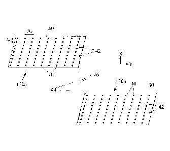
Figure 3 shows schematically, and to a much enlarged scale, the relative
positioning of two
laser emitting element arrays 130a and 130b of VCSEL chips 30 that are
adjacent one another in
the Y-direction but are located in different rows. Each of the chips has a
regular array of M by N
laser emitting elements 40, as previously described, that are represented by
circular dots. In the
example illustrated, M and N are equal, there being nine rows and nine
columns. The spacing
between the elements in a row, designated Ar, and the spacing between the
elements in a column,
designate ac, are shown as being different from one another but they may be
the same. The array
is shown as being slightly skewed so that the columns and rows are not
perpendicular to one
another. Instead, the rows lie parallel to the Y-direction while the columns
are at a slight angle to
the X-direction. This enables lines, such as the lines 44, traced by the
elements 40 on the imaging
surface, if energized continuously, to be sufficiently close together to allow
high resolution images
to be printed. Figure 3 shows that the element at the end of each row traces a
line that is a distance
Ar/M away from the line traced by the corresponding element of each adjacent
row, the separation
between these lines being the image resolution I,. Thus A, and M are selected
in dependence upon
.. the desired image resolution, based on the equation A, = M x Jr.
It should be mentioned that it is possible for the elements to lie in a square
array where the
columns are perpendicular to the rows. In this case, the chips would need to
be mounted askew on
their support and compensation would need to be applied to the timing of the
control signals used
to energize the individual elements.
As is clear from Figure 3, and also Figure 5B which shows the traced lines to
a larger
scale, the positioning of the array 130b is such that the line traced by its
bottom left element 40
should ideally also be spaced from the line traced by the top right element of
the array
17
CA 2986370 2021-05-26
CA 02986370 2017-11-17
WO 2016/189510 PCT/IB2016/053137
18
130a by a distance equal to AT/M. Therefore when all the elements 40 of both
arrays 130a and
130b are energized, they will trace 2=M=N lines that will all be evenly spaced
apart by a
distance Ar/M between adjacent lines, without any gaps.
If one wishes to provide compensation for defective elements, the array could
include
additional rows of laser emitting elements 40, but it is alternatively
possible to compensate for
a defective element by increasing the intensity of the laser beams generated
by the laser
emitting elements that trace the two adjacent parallel lines.
In addition to the M by N array of elements 40, each chip has two additional
columns
that are arranged one each side of the main array, each containing a
respective further element
42. These further elements 42 are represented in Figure 3 by stars, to
distinguish them from
the main array elements 40. The additional laser elements on each side of each
array, can be
positioned at a distance of 1/3 the spacing between traced lines that are
imaged by the lenses
onto the imaging surface. Furthermore additional elements could be placed in
the gap between
two arrays that nominally spans a distance of Ar/M so that higher sensitivity
is achieved in
correcting the spacing errors between adjacent arrays.
As can be seen from Figure 3 and Figure 5B, when activated, these elements 42
trace
two additional lines 46 between the two sets of evenly spaces parallel lines
44a and 44b
traced by the elements 40 of the two arrays 130a and 130b, respectively.
One of the additional lines 46 is spaced by a distance Ar/3M from the last
adjacent line
44a traced, for example, by the array 130a in Figure 3 and the other is spaced
by a distance
Ar/3M from the first adjacent line 44b traced, for example, by the array 130b.
In the event of
a misalignment between the two arrays 130a and 130b these elements 42 can be
energized in
addition to, or instead of some of, the elements 40 of the main arrays to
compensate for any
misalignment between the arrays 130a and 130b that tends to create a stripe in
the printed
image, be it a gap or a dark line resulting from an overlap. Figure 5A, which
is similar to
Figure 5B, shows the alternative approach proposed in the prior art to
compensate for chip
misalignment. In the prior art, each chip has an additional row of elements
that produces
traced lines that are interlaced with the traced lines of the adjacent chip,
resulting in a very
high degree of redundancy.
While the two additional elements 42 in the present proposal are shown in
Figure 3 and
Figure 5B as tracing two separate lines 46, the energies of these two elements
can be
combined on the imaging surface, as earlier described, to form a single line
of which the
position is controllable by appropriate setting of the energies emitted by
each of the additional
elements 42. This is shown in Figures 6 in which the energy profiles of the
lines 44a and 44b are
designated 94a and 94b, respectively and the energy profiles of the additional
lines 46 are
designated 96a and 96b. In Figure 6, neither of the profiles 96a and 96b
(shown in dotted lines)
has sufficient energy to render the coating particles tacky but at the
centerline between the two
arrays the cumulative energy, shown as a solid dark line 96, is sufficient to
soften the particles
coating and to create a trace line filling the gap between the trace lines 44a
and 44b of the two
main arrays.
While in Figure 6 the energy profiles of the two additional elements are
matched, it is
possible by varying the relative intensity of the two beams emitted by the
additional laser sources
to position the centerline of the combined energy at a different distance from
the traces of the main
arrays.
Figure 7A shows how the ability to create dots that do not fall on the
centerlines of the
energy profiles of the laser elements can be used to advantage to achieve anti-
aliasing. Figure 7A
shows the energy profiles of four adjacent elements of the main array. The
first two profiles a and
b are set at a desired level, say 8 (out of sixteen), corresponding to mid-
grey. The energy profiles
c and d, on the other hand are set to say 12 and 4, respectively. The
resulting dot pattern produced
on the imaging surface is shown in Figure 7B. This can be seen to comprise two
regular sized
dots A and B aligned with the line of symmetry of the profiles a and b in
Figure 7A, a larger sized
dot C aligned with the centerline of energy profile c, and a smaller dot D
that lies somewhere
between the centerlines of the profiles c and d.
The result of repeating such a dot pattern diagonally is shown in Figure 8A.
When this image
is compared with Figure 8B, where no anti-aliasing steps have been taken, it
will be seen that the
small dots in between regular raster line yield oblique edges that have
reduced jaggedness and
produce an image that is comparable with one achievable by a printing system
having a greater
image resolution.
The interaction of energies from nearby laser elements can also be used to
compensate for
missing elements in that the elements producing the two adjacent raster lines
can be used to
combined in the same manner as previously explained to fill in a gap between
them.
For the arrays 130a and 130b in Figure 3 to function correctly as described
above, their relative
position in the Y-direction is critical. In order to simplify the construction
of the lens system
serving to focus the emitted laser beams on the imaging surface it is
advantageous to
19
CA 2986370 2021-05-26
CA 02986370 2017-11-17
WO 2016/189510 PCT/IB2016/053137
adopt a configuration shown in Figure 4 which enables the two rows of lenses
corresponding
to a pair of chip rows to be self-aligning.
Figure 4 shows seven adjacent arrays 130 each shown lined up with a respective
lens
18. Though arrays 130 can as afore-mentioned include additional laser elements
42, such are
5 not shown on the present figure. Each lens 18 is constructed as a GRIN
(Gradient-Index) rod,
this being a known type of lens that is shaped as a cylinder having a radially
graduated
refractive index. In the case of the geometry shown in Figure 4, corresponding
elements of
any three bi-directionally adjacent arrays 130 lie on the apices of an
equilateral triangle, three
such triangles designated 50 being shown in the drawing. It will be noted that
all the triangles
10 50 are congruent. As a result, if the diameter of the GRIN rods is now
selected to be equal to
2-1\1=Ar, which is the length of the sides of the equilateral triangles 50, or
the distance between
corresponding laser emitting elements of adjacent VCSEL chips 30 in the same
row, then
when stacked in their most compact configurations, the lenses 18 will
automatically align
correctly with their respective chip.
15 Though the lens 18 has been schematically illustrated in Figure 1 (side
view) and
Figure 4 (cross section view) as being an individual GRIN rod, in an
alternative embodiment
shown in Figure 9 the laser beams of each chip can be transmitted by a series
of lenses. In the
case of Figure 9, the single GRIN rod 18 is replaced by two mutually inclined
GRIN rods 18a
and 18b and the light from one is directed to the other by a prism 87 of high
refractive index
20 .. glass, so that the light follows a folded path. Such a configuration
enables coating stations in
a colour printing system to be arranged closer to one another in a more
compact
configuration. Such a folded light path can adopt different configurations
while fulfilling all
the requirements of magnification and light transmission. To enable the light
path to be split
in this manner, the length of the GRIN rods is selected such that light is
collimated on leaving
the rods 18a and entering the rods 18b as shown by the light rays drawn in
Figure 9.
The radiation guided by GRIN rod 18a, the proximal end of which is arranged at
a
distance WD,, from the chip, may be captured by the corresponding GRIN rod 18b
which can
collect the collimated light emerging from rod 18a on the same light path and
focus it at a
distance WDi from the distal end of the second GRIN rod 18b. When the two GRIN
rods are
made of the same material and the same radial gradient profile and WID,, = WD,
a
magnification of M=+1 can be obtained.
Laser elements that are away from the longitudinal axis of the GRIN rod 18a
will leave
the distal end of the GRIN lens collimated but at an angle to the axis. In
certain cases, it is
CA 02986370 2017-11-17
WO 2016/189510 PCT/IB2016/053137
21
necessary for the distance between the two rods 18a and 18b to be large,
causing the off axis
collimated beams exiting the first rod segment to miss partially or entirely
the second
segment. It is possible to take advantage of Snell's law and cause the beam
exiting the first
rod to travel through a glass with a high refractive index, thus causing the
angle the collimated
beam makes with the optical axis to decrease and enabling a larger separation
between the
rods before the collimated beams leaving the first rod miss the entrance to
the second rod.
In the description and claims of the present disclosure, each of the verbs,
"comprise"
"include" and "have", and conjugates thereof, are used to indicate that the
object or objects of
the verb are not necessarily a complete listing of members, components,
elements, steps or
parts of the subject or subjects of the verb. These terms encompass the terms
"consisting of'
and "consisting essentially of'.
As used herein, the singular form "a", "an" and "the" include plural
references and
mean "at least one" or "one or more" unless the context clearly dictates
otherwise.
Positional or motional terms such as "upper", "lower", "right", "left",
"bottom",
"below", "lowered", "low", "top", "above", "elevated", "high", "vertical",
"horizontal",
"backward", "forward", "upstream" and "downstream", as well as grammatical
variations
thereof, may be used herein for exemplary purposes only, to illustrate the
relative positioning,
placement or displacement of certain components, to indicate a first and a
second component
in present illustrations or to do both. Such terms do not necessarily indicate
that, for example,
a "bottom" component is below a "top" component, as such directions,
components or both
may be flipped, rotated, moved in space, placed in a diagonal orientation or
position, placed
horizontally or vertically, or similarly modified.
Unless otherwise stated, the use of the expression "and/or" between the last
two
members of a list of options for selection indicates that a selection of one
or more of the listed
options is appropriate and may be made.
In the disclosure, unless otherwise stated, adjectives such as "substantially"
and "about"
that modify a condition or relationship characteristic of a feature or
features of an
embodiment of the present technology, are to be understood to mean that the
condition or
characteristic is defined to within tolerances that are acceptable for
operation of the
embodiment for an application for which it is intended.
While this disclosure has been described in terms of certain embodiments and
generally
associated methods, alterations and permutations of the embodiments and
methods will be
CA 02986370 2017-11-17
WO 2016/189510 PCT/IB2016/053137
22
apparent to those skilled in the art. The present disclosure is to be
understood as not limited
by the specific embodiments described herein.