Note: Descriptions are shown in the official language in which they were submitted.
16-CWD-983 CA
CURRENT SHARING ARCHITECTURE FOR COMBINATION CHARGER
BACKGROUND
Field
The disclosed concept pertains generally to chargers for charging
electrical devices, and, more particularly, to a combination charger that
includes a current
sharing architecture for multiple types of output ports, such as USB Type-A
and USB
Type-C ports.
Background Information
USB-C is the emerging industry-standard connector for transmitting both
data and power, and will likely be the next generation of cross-platform
connectors. As a
result, it is likely that next generation electrical devices coming to the
market will have
both USB Type-C ports/connectors and traditional USB Type-A ports/connectors.
There will thus be need for a combination charger that is able to charge
devices having either a USB Type-C port/connector or a traditional USB Type-A
port/connector as needed.
SUMMARY
In one embodiment, a charger apparatus is provided that includes a
housing, a first port supported by the housing, a second port supported by the
housing
that is different than the first port, a first circuit coupled to the first
port and structured to
advertise a first current at the first port, and a second circuit coupled to
the second port
and structured to advertise a second current at the second port. The charger
also includes
a controller, wherein the first circuit and the second circuit each receive a
DC power
signal generated from an AC input signal provided to the charger apparatus,
and wherein
the controller is structured and configured to determine whether a load
current on the
second circuit is above a threshold level and responsive to determining that
the load
current on the second circuit is above the threshold level, (i) cause the
first circuit to
advertise the first current at a level that is less than a maximum current
level that may be
advertised at the first port, and (ii) cause the second circuit to advertise
the second current
at a level that is equal to a maximum current level that may be advertised at
the second
port.
1
CA 2986548 2017-11-23
16-CWD-983 CA
In another embodiment, a method of controlling a charger apparatus that
includes a first port and a second port of a different type than the first
port is provided.
The method includes receiving a DC power signal generated from an AC input
signal
provided to the charger apparatus, determining whether a load current being
provided to
the second port is above a threshold level, and responsive to determining that
the load
current being provided to the second port is above the threshold level, (i)
causing the first
port to advertise a first current at a level that is less than a maximum
current level that
may be advertised at the first port, and (ii) causing the second port to
advertise a second
current at a level that is equal to a maximum current level that may be
advertised at the
second port.
BRIEF DESCRIPTION OF THE DRAWINGS
A full understanding of the disclosed concept can be gained from the
following description of the preferred embodiments when read in conjunction
with the
accompanying drawings in which:
FIG. 1 is a schematic diagram of a combination charger apparatus
according to an exemplary embodiment of the disclosed concept;
FIG. 2 is a schematic diagram showing a first portion of the combination
charger apparatus of FIG. 1; and
FIG. 3 is a schematic diagram showing a second portion of the
combination charger apparatus of FIG. 1.
DESCRIPTION OF THE PREFERRED EMBODIMENTS
Directional phrases used herein, such as, for example, left, right, front,
back, top, bottom and derivatives thereof, relate to the orientation of the
elements shown
in the drawings and are not limiting upon the claims unless expressly recited
therein.
As used herein, the term "number" shall mean one or an integer greater
than one (i.e., a plurality).
As used herein, the statement that two or more parts are "coupled"
together shall mean that the parts are joined together either directly or
joined through one
or more intermediate parts.
2
CA 2986548 2017-11-23
16-CWD-983 CA
As used herein, the term "controller" means a programmable analog
and/or digital device (including an associated memory part or portion) that
can store,
retrieve, execute and process data (e.g., software routines and/or information
used by
such routines), including, without limitation, a programmable system on a chip
(PSOC), a
field programmable gate array (FPGA), a microprocessor, a microcontroller, a
programmable logic controller, or any other suitable processing device or
apparatus. The
memory portion can be any one or more of a variety of types of internal and/or
external
storage media such as, without limitation, RAM, ROM, EPROM(s), EEPROM(s),
FLASH, and the like that provide a storage register, i.e., a non-transitory
machine
readable medium, for data and program code storage such as in the fashion of
an internal
storage area of a computer, and can be volatile memory or nonvolatile memory.
As USB-C emerges as the next generation platform, combination charger
devices that are capable of charging through both USB-C and USB-A connections
(separately or at the same time) will become advantageous. Such chargers,
however, will
likely have design constraints (based on, for example, the charger form
factor) that limit
the total current that is available for charging at any one time (e.g., to a
total of 4.5A
being available). As will be appreciated, that total current will have to be
shared between
the Type-A and Type-C ports/connections of the charger. This means that only
of the
connected devices can get the "maximum" current (e.g., 3A) at any one time,
while the
other device has to settle for less current (e.g., 1.5A).
Most existing electrical devices, however, utilize a USB Type-A port for
charging. Thus, in the near future, it will be more likely that a Type-A
device will be
plugged in to such a combination charger for charging than a Type-C device.
The
disclosed concept thus provides an innovative charging architecture that
automatically
assigns the current priority to Type-A devices over Type-C devices by sensing
the load
current. As Type-C devices become more prevalent, the same architecture may be
used
with minor modifications to assign the current priority to Type-C devices over
Type-A
devices by sensing load current.
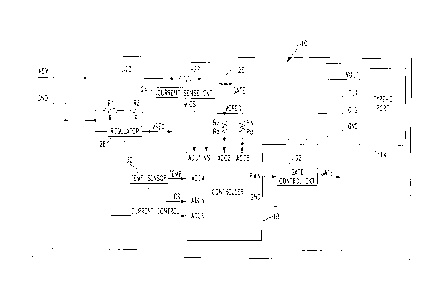
FIG. 1 is a schematic diagram of a combination charger apparatus 2
according to an exemplary embodiment of the disclosed concept. Combination
charger
apparatus 2 implements the priority charging architecture described above and
thus has
3
CA 2986548 2017-11-23
16-CWD-983 CA
the ability to charge through both USB-C and USB-A connections. Combination
charger
apparatus 2 includes a housing 4 for housing the components thereof.
Combination
charger apparatus 2 further includes an AC power plug 6 for connecting
combination
charger apparatus 2 to an AC source, such as a wall outlet, in order to
provide AC input
power to combination charger apparatus 2.
Combination charger apparatus 2 further includes a rectifier and signal
conditioning circuit 8 that is provided within housing 4. Rectifier and signal
conditioning
circuit 8 receives the AC input power from AC power plug 6 and converts it
into DC
power of an appropriate level. In the illustrated embodiment, rectifier and
signal
conditioning circuit 8 converts the AC input power in to +5V and ground.
Alternatively,
rectifier and signal conditioning circuit may be replaced by, for example,
without
limitation, a low dropout (LDO) regulator, a switch mode power supply (SMPS),
or any
other power supply. As seen in FIG. 1, combination charger apparatus 2 further
includes
a Type-C circuit 10 and a Type-A circuit 12, each of which is described in
greater detail
herein. Type-C circuit 10 and Type-A circuit 12 each receive the DC output of
rectifier
and signal conditioning circuit 8. Combination charger apparatus 2 further
includes a
USB Type-C port 14 and a USB Type-A port 16 to enable both Type-C and Type-A
devices to be selectively connected to combination charger. apparatus 2 for
charging
purposes.
As described in greater detail herein, in the exemplary embodiment, Type-
C circuit 10 and Type-A circuit 12 together implement a current priority
scheme wherein
Type-A is given current priority over Type-C. More specifically, in the scheme
of the
exemplary embodiment, combination charger apparatus 2 monitors Type-A port 16
to
determine whether and when a device is connected thereto or when a device is
connected
and requesting more charge. If combination charger apparatus 2 detects that a
device is
not connected to Type-A port 16 or the device is drawing more current than a
set
threshold (by sensing load current as described herein), combination charger
apparatus 2
is configured such that Type-C port 14 will advertise a maximum current level
(e.g., 3A)
and Type-A port 16 will advertise a lower set current level (e.g., 1.5A).
Conversely, if
combination charger apparatus 2 detects that a device is connected to Type-A
port 16
(again by sensing load current as described herein), combination charger
apparatus 2 is
4
CA 2986548 2017-11-23
16-CWD-983 CA
configured such that Type-A port 16 will automatically advertise a maximum
current
level (e.g., 3A) and Type-C port 14 will automatically advertise a lower set
current level
(e.g., 1.5A).
FIG. 2 is a schematic diagram showing Type-C circuit 10 according to the
exemplary embodiment. Referring to FIG. 2, Type-C circuit 10 includes a
controller 18
that is structured and configured to control the operation of combination
charger
apparatus 2 as described in detail herein (e.g., controller 18 is provided
with one or more
routines for this purpose). Type-C circuit 10 further includes a power rail 20
that
receives the positive DC voltage from rectifier and signal conditioning
circuit 8. A sense
resistor 22 is provided in power rail 20. A current sense circuit 24 is
coupled to power rail
in order to sense the current that is flowing through power rail 20 at any
particular
time by sensing the voltage drop across sense resistor 22. The output of
current sense
circuit 24 is provided to controller 18.
Power rail 20 further includes an electronic switch 26 (e.g., a MOSFET)
15 that is provided between sense resistor 22 and Type-C port 14. In
addition, a regulator
circuit 28 is coupled to power rail 20 and provides a regulated input voltage
(Vreg) that is
used to power controller 18. A temperature sensor 30 is also provided in Type-
C circuit
10. Temperature sensor 30 is powered by Vreg and senses the board temperature
of
Type-C circuit 10. The measured board temperature is provided to controller
18.
20 Controller 18 is structured to shut Type-C circuit 10 down in the case
of an over-
temperature condition. The measured board temperature may also be used for
thermal
cycling of the operation of controller 18 if needed. In particular, a high
temperature input
can be used to scale down the charge current value, until the temperature
reaches a safe
limit.
A gate control circuit 32 is connected to controller 18. The output of gate
control circuit 32 is provided to electronic switch 26. Controller 18 is
structured to
generate pulse width modulation (PWM) pulses which are provided to gate
control circuit
32. Based upon the received PWM pulses, gate control circuit 32 will control
electronic
switch 26 and therefore control the current that is provided to Type-C port
14. As shown
in FIG. 2, controller 18 is also operatively coupled to Type-C 14 for data
transmission
purposes.
5
CA 2986548 2017-11-23
16-CWD-983 CA
FIG. 3 is a schematic diagram showing Type-A circuit 12 according to the
exemplary embodiment. Referring to FIG. 3, Type-A circuit 12 includes a power
rail 34
that also receives the positive DC voltage from rectifier and signal
conditioning circuit 8.
As seen in FIG. 3, Vreg from regulator 28 is used to generate a reference
voltage using a
voltage divider circuit 36. The reference voltage is provided to a comparator
38 that is
provided as part of Type-A circuit 12. The output of comparator 38 forms a
current
control signal that is provided as an input to controller 18 (FIG. 2).
In operation, the load current irt Type-A circuit 12 is monitored using
comparator 38, and the output thereof is used to determine how combination
charger
apparatus 2 is configured at any given time. In particular, if the load
current in Type-A
circuit 12 exceeds a predetermined threshold value (indicating that a device
is connected
to Type-A port 16 or requesting more current than a set current threshold
value), the
output of comparator 38, i.e., the current control signal, will go low. When
controller 18
senses that the current control signal has gone low, controller 18 adjusts the
PWM pulses
provided to gate control circuit 32 in a manner that causes type-C-port 14 to
change from
advertising the maximum current level (e.g., 3A) (the default state) to
advertising the
lower set current level (e.g., 1.5A). In addition, under these conditions,
Type-A port 16
will be caused to advertise the maximum current level (e.g., 3A). If the load
current in
Type-A circuit 12 drops below the predetermined threshold (indicating that a
device is
not connected to Type-A port 16 or is requesting less current than the set
current
threshold value), the output of comparator 38, i.e., the current control
signal, goes high.
In response, if the Type-C circuit 10 current is determined to be above a
threshold level
based upon the output of current sense circuit 24, controller 18 will adjust
the PWM
pulses provided to gate control circuit 32 to cause Type-C port 14 to be
configured to
again advertise the maximum current level (e.g., 3A), and Type-A port 16 will
be caused
to advertise the lower set current level (e.g., 1.5A).
In an alternative embodiment, the current threshold levels described herein
may be configurable by a user, such as by using a potentiometer or by any
other suitable
means, to give the user an option to select their own current threshold
levels.
While specific embodiments of the disclosed concept have been described
in detail, it will be appreciated by those skilled in the art that various
modifications and
6
CA 2986548 2017-11-23
16-CWD-983 CA
alternatives to those details could be developed in light of the overall
teachings of the
disclosure. Accordingly, the particular arrangements disclosed are meant to be
illustrative only and not limiting as to the scope of the disclosed concept
which is to be
given the full breadth of the claims appended and any and all equivalents
thereof.
7
CA 2986548 2017-11-23