Note: Descriptions are shown in the official language in which they were submitted.
CA 02990283 2017-12-20
WO 2017/004704
PCT/CA2016/050769
SELF-ALIGNING METAL PATTERNING BASED ON PHOTONIC
SINTERING OF METAL NANOPARTICLES
TECHNICAL FIELD
[0001] The present disclosure relates generally to fabrication techniques
for
printable electronic devices and, in particular, to a technique for aligning
layers in
fabricating a multilayer printable electronic device.
BACKGROUND
[0002] Printing functional inks on flexible and low-cost substrates is an
increasingly popular method of fabricating electronic devices. A multilayer
printing
process, which is frequently utilized in fabricating electronic devices,
remains
challenging because it is difficult to achieve the required alignment or
registration
precision when an upper layer is printed over an under layer. To address the
issues
in layer-to-layer alignment accuracy, a self-alignment process was proposed
(Pa!finger et al., Adv. Mater. 2010, 22, 5115-5119) for printing organic
transistors. In
this method, the first metal layer is patterned by nano-imprint lithography or
a micro-
contact printing process followed by a wet etching step. This patterned metal
layer
later acts as a mask to pattern the next metal layer via a traditional or a
roll-to-roll
(R2R) photo-lithography process and a lift-off step. However, in this proposed
self-
alignment process, metal layers are vacuum evaporated, and several photo-
lithography, wet-etching, and lift-off steps are required. To make the self-
alignment
process truly compatible with R2R printing process, it is desirable to have
metal
layers, which are printable and patternable using minimum wet steps.
[0003] UV-curable metal inks, which are UV-curable resins filled with metal
particles, are potential candidates for use in a self-alignment process to
replace the
vacuum deposited metal layers. However, there are serious drawbacks in using
UV-
curable metal inks in the self-alignment process. Firstly, UV-curable metal
inks
contain photo initiators and cross-linkers, which remain in the film and
reduce the
conductivity of the resulting metal film. Secondly, printed metal films are
opaque,
the UV penetration depth is very limited in this kind of film, and the
thickness that
- 1 -
CA 02990283 2017-12-20
WO 2017/004704
PCT/CA2016/050769
can be cross-linked is also very limited. Thirdly, the achievable patterning
resolution
of the inks is fundamentally limited to the size of its metal particles.
[0004] Accordingly, a new or improved self-aligning technique would be
highly
desirable in order to facilitate fabrication of multilayer printable
electronic devices.
SUMMARY
[0005] The present disclosure provides a new self-aligning technique for
fabricating multi-layer printable electronic devices. This method enables high-
precision alignment of the metal pattern printed on the upper layer with the
ink
pattern on the lower or under layer. A metal nano particle ink or any other
equivalent ink acts as a negative photoresist so that the first metal layer
printed or
deposited on a transparent substrate can act as a mask. Intense light pulses
are
then applied from the backside of the substrate to partially sinter the metal
nano
particles that are exposed. The metal nano-particles in the shaded area are
not
sintered and thus can be washed away. Partially sintered particles are then
fully
sintered in a post sintering step. Partially sintering involves exposing the
particles
to the minimum required optical power with the shortest pulses to minimally
sinter
the exposed particles so they are just barely connected to the functional
layer to
resist washing off the functional layer during subsequent washing.
[0006] Accordingly, one inventive aspect of the present disclosure is a
method
for aligning metal layers in fabricating a multilayer printable electronic
device. The
method entails providing a transparent substrate upon which a first metal
layer is
deposited, providing a transparent functional layer over the first metal
layer,
depositing metal nano particles over the functional layer to form a second
metal
layer, exposing the metal nano particles to intense pulsed light via an
underside of
the substrate to partially sinter exposed particles to the functional layer
whereby the
first metal layer acts as a photo mask, and washing away unexposed particles
using
a solvent to leave partially sintered metal nano particles on the substrate.
The
functional material may be a conductor, semiconductor, dielectric,
electroluminescent, photovoltaic, or any other electronic function.
[0007] This summary is provided to highlight certain significant inventive
aspects
but is not intended to be an exhaustive or limiting definition of all
inventive aspects
- 2 -
CA 02990283 2017-12-20
WO 2017/004704
PCT/CA2016/050769
of the disclosure. Other inventive aspects may be disclosed in the detailed
description and drawings.
BRIEF DESCRIPTION OF THE DRAWINGS
[0008] Further features and advantages of the present technology will
become
apparent from the following detailed description, taken in combination with
the
appended drawings, in which:
[0009] Figure 1 illustrates an example of how metal nano particles are used
as a
negative photoresist,
[0010] Figure 2 illustrates, by way of example, a method of self-aligning
metal
patterning based on the photo sintering of metal nano particles;
[0011] Figure 3A illustrates a dried coating of silver nano particle ink
produced
on PET film;
[0012] Figure 3B illustrates the coating of silver nano particles on PET
after the
sample was exposed to intense pulsed light under another PET film bonded with
dark tape strips on its upper surface;
[0013] Figure 30 illustrates the coating of silver nano particles on PET
when the
exposed sample is immersed into dehydronapthalene for development;
[0014] Figure 3D illustrates the coating that remains after the unexposed
sample
was washed with dehydronapthalene,
[0015] Figure 4A illustrates the pre-existing silver pattern of silver nano
particles
coating on PET;
[0016] Figure 4B illustrates the coating formed of silver nano particles on
the
opposite side of the above PET after the sample was exposed to light from the
side
with the pre-existing silver pattern and washed with a solvent;
[0017] Figure 5A illustrates a pre-existing silver pattern formed of silver
nano
particles on one side of PET;
- 3 -
CA 02990283 2017-12-20
WO 2017/004704
PCT/CA2016/050769
[0018] Figure 5B illustrates the pattern of silver nano particles on the
opposite
side after the sample was exposed to light from the patterned side and washed
with
a solvent;
[0019] Figures 6A-6D depict the processed coating of silver nano particle
ink on
PET film wherein the coating, before being developed in water, was exposed to
intense pulsed light from the back side of the PET which was previously
printed with
a silver pattern;
[0020] Figures 7A and 7B depict a coating of silver nano particles on PET
film
wherein the coating was exposed to intense pulsed light from a back side of
its
substrate;
[0021] Figures 8A and 8B depict a coating of silver nano particle ink on a
PMMA-
covered PET film wherein 300nm PMMA was coated on the PET with the printed
silver pattern and the sample was exposed to intense pulsed light from the
back side
of the PET with subsequent development carried out in water;
[0022] Figures 9A and 9B depict a coating of silver nano particle ink on
PMMA-
covered PET film wherein 300nm PMMA was coated on a PET surface with the
printed silver pattern and the sample was exposed to intense pulsed light from
the
back side of the PET and the subsequent development was carried out in
ethanol;
and
[0023] Figures 10A and 10B depict a line of silver nano particle ink on a
PMMA-
covered PET film wherein the line of ink was printed on 300nm-PMMA on PET film
using an inkjet printer and the light exposure was from the back side of the
PET film
and the development was carried out in water.
[0024] It will be noted that throughout the appended drawings, like
features are
identified by like reference numerals.
DETAILED DESCRIPTION
[0025] Disclosed herein is a method (or process) of using a photonic
sintering
process and metal nano particle inks for self-alignment metal patterning. This
method obviates the need for multiple photolithography steps or for metal
vacuum
- 4 -
CA 02990283 2017-12-20
WO 2017/004704
PCT/CA2016/050769
deposition. High-precision alignment between the metal pattern in the upper
layer
and the lower and under layer is achieved by using the metal nano particle ink
as a
negative photoresist. The first metal layer printed on a transparent substrate
acts as
a mask to block light applied from the back side of the substrate. The intense
light
pulses applied from the backside of the substrate partially sinter the nano
particles
that are exposed, i.e. not covered by the mask. The metal nano-particles that
are
masked are unaffected by the sintering and thus can be washed away.
[0026] The method is primarily intended for use in fabricating electronic
devices
having a multilayer structure by printing or an equivalent low-cost deposition
process. Many electronic devices require a multilayer structure, in which the
pattern
of one of the upper layers has to be precisely aligned with the pattern in the
layer
underneath in order to function correctly or optimally. For instance, a
transistor
requires that the metal electrodes in the upper layer be precisely aligned
with the
ones in the layer underneath. The method disclosed herein uses photonic
sintering
of metal nano particles to precisely align the metal pattern in the upper
layer with the
metal pattern in the layer beneath. In other words, this method facilitates
fabrication
of multilayer printable electronic device which require precise alignment of
the upper
and lower layers.
[0027] Metal nano particles exhibit strong plasmonic absorption in the
wavelength range from UV to near IR, and thus can be heated by light. Metal
nano
particles also have very low melting temperature because of their nano size
and
thus can be sintered at a very low temperature such as, for example, 120 C. As
such, it is possible to use the heat generated by the plasmonic absorption to
sinter
the particles onto the substrate. Both laser and intense pulsed light may be
used to
directly irradiate and thus sinter metal nano-particle particles to produce
coatings
and patterns on the substrate.
[0028] The photonic sintering of metal nano particles can cause the
individual
particles to form a dense metal film. This process is somewhat similar to the
UV-
caused crosslinking of a polymer, which makes the polymer insoluble. However,
there are a few fundamental differences between the two: 1) the UV-
crosslinking
reaction is directly caused by the photons in the UV light, and therefore the
cross-
linking depth is limited by the depth of light penetration. In the case of
printed metal
- 5 -
CA 02990283 2017-12-20
WO 2017/004704
PCT/CA2016/050769
films, the cross-linking depth is limited to the surface area; while the
sintering of the
metal nano particles are caused by the local heat generated by the intense,
short
light pulses. Although the light pulse is also limited in depth of
penetration, the heat
generated by the light pulses can transfer over a reasonable range (100's nm).
This
transfer range is sufficiently large to sinter metal films used in typical
printable
electronics (having a typical thickness of -100's nm). Moreover, photonic
sintering
yields very good lateral patterning resolution (100's nm vs 10's p.m).
Furthermore,
the heat transfer range can be controlled by varying the pulse intensity,
frequency
and duration; 2) the UV-crosslinking process requires photo initiators and
cross-
linkers, which will remain in the films and affect their properties. In
contrast, the
sintering of the metal nano particles is basically a particle melting process,
such that
the resulting films have properties very similar to the bulk material; 3) the
UV-
crosslinking process uses the inks that are based on the UV curable polymer
filled
with metal particles, normally several micrometers in diameter or length. The
achievable patterning resolution cannot be smaller than the particle size.
[0029] Figure 1 illustrates a method of using metal nano particles to
function as a
negative photoresist. The metal nano particles are first deposited on the
substrate
by a suitable deposition method, such as coating or printing, using metal nano
particle-suspended liquid, or so-called nano ink. After the particles have
dried, the
particles are exposed to intense pulsed light, through a photo mask, whose
wavelength substantially covers or matches that of the plasmonic absorption of
the
particles. The exposed particles are partially sintered by the absorbed energy
to
thereby adhere to the substrate when a solvent is used to wash away the
unexposed particles in the development process. Finally, a post sintering
process is
performed to fully sinter the particles onto the substrate to become a dense
metal
film with desired performance characteristics.
[0030] Figure 2 illustrates the self-alignment method for metal patterning.
The
method employs photonic sintering of metal nano particles. The nano particle
ink is
deposited on the substrate surface with the first metal pattern underneath,
either
separated by a transparent layer of material for special functions or by the
substrate
itself. The light is shined from the back side of the substrate. The metal
pattern on
the under layer acts as a photo mask. Exposed particles adhere to the
substrate due
- 6 -
CA 02990283 2017-12-20
WO 2017/004704
PCT/CA2016/050769
to photonic-induced partial sintering. These partially sintered particles
remain on the
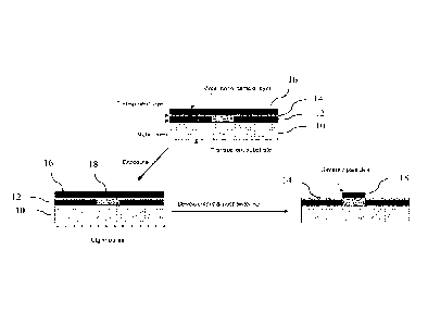
surface through the development process. After being thermally annealed, the
remaining material, which is precisely aligned to the pre-existed metal
pattern, is
fully sintered in a post sintering process to obtain the desired performance
characteristics, such as conductivity. Figure 2
shows the structure of a stack
composed of a transparent substrate 10 upon which a first metal layer 12 is
deposited, a transparent functional layer 14 over the first metal layer, and a
second
metal layer 16 that is formed by depositing metal nano particles on the
transparent
functional layer 14. The metal nano particles are then partially photonically
sintered
to leave partially sintered particles 18 that form a pattern or line that
remain after the
second metal layer is washed with an appropriate solvent. The sintered
particles 18
that remain after sintering are aligned with the first metal layer. The
functional layer
is made of a functional material which may be a conductor, semiconductor,
dielectric, electroluminescent, photovoltaic, or any other electronic
function.
[0031] Photonic
sintering of metal nano particles is fundamentally different from
the conventional UV-induced photo crosslinking of polymer widely used in
photolithography-based fabrication techniques. The conventional UV-induced
photo
crosslinking process relies on light penetration in the film to be cured. The
UV light
does not penetrate well in a printed metal film. In the present method, the
photonic
sintering patterning process is fundamentally still a sintering process, in
which
particles are fused together at their surfaces through the heat generated by
the
plasmonic absorption of the metal nano particles. The heat may be quickly
transferred from the exposed particles to adjacent unexposed particles, due to
the
high thermal conductivity of metal, causing sintering in the unexposed area,
both in
the thickness direction and side direction of the nano particle coating. This
effect is
critical in sintering particles through the whole coating thickness, but may
also cause
the sintering in the masked edge area and thus reduce the patterning
resolution. In
order to minimize this negative effect, the present method employs partial
sintering.
It uses the minimum required optical power with the shortest pulses to
minimally
sinter the exposed particles so they are just barely connected or fused to the
level
that they become resistant to the solvent used to disperse or suspend the nano
particles and have a sufficient adhesion on the substrate. With this, the
unexposed
- 7 -
CA 02990283 2017-12-20
WO 2017/004704
PCT/CA2016/050769
nano particles can be easily and cleanly washed away with the solvent used to
disperse the particles in their original liquid sample or ink, and the exposed
ones will
stay on the substrate. The desired performance characteristic, such as
electrical
conductivity, of the obtained film formed by the partially connected nano
particles
might be poor at this stage, but can be dramatically improved to the
application-
required level after the particles are fully sintered in a post sintering
process.
[0032] The method was demonstrated by coating a thin layer of silver nano
particles on a piece of DuPont PET film (Melinex ST 505) and exposing the
coating
to intense pulsed light under another piece of PET film with dark polymer tape
strips
bonded on its upper surface. In this first example (Example 1) the coating of
silver
nano particles on PET film was prepared using XF-1 silver nano ink produced by
Xerox research center in Canada (XRCC) and the blade coating equipment
(509MC) of Erichsen, and dried at room temperature (as shown by Figure 3A).
Another piece of PET film with bonded dark tape strips on its upper surface
was
used as a photo mask and placed on top of the coated PET film as illustrated
by
way of example in Figure 1. After the nano-particle coating was exposed to the
programmed intense pulsed light (2.4kV, double exposure at 200 microseconds
for
each one, with a plate displacement of 5 mm in each cycle) in the photonic
curing
R&D system (Sinteron 2000 from Xenon Corporation) through the above mask, the
lit part turned a gold color, while the blocked and thus unexposed parts kept
their
original color (as shown in Figure 3B). When the sample was immersed into
dehydronapthalene, the unexposed parts turned a black color instantly (as
shown in
Figure 3C) and gradually diffused into the solvent. The transparent PET was
recovered in the unexposed area to show the corresponding patterns of the dark
tape strips, after the unexposed silver particles were completely washed away
with
sharp edges left in the remaining coating (as shown in Figure 3D). The
resistance of
the remaining coating (which was 660 nm thick) was measured to be in the range
of
30 to 60 ka between two adjacent corners. The resistance value dropped to 0.9
to
1.3 Q after the sample was thermally annealed at 130 C for 30 minutes.
[0033] To apply the method above in self-aligning silver patterning as
illustrated
by way of example in Figure 2, the effect of the substrate should be
considered. As
light travels through the coating substrate before reaching the nano particle
coating,
- 8 -
CA 02990283 2017-12-20
WO 2017/004704
PCT/CA2016/050769
its energy may be partially absorbed by the substrate and converted to heat.
This
heat can combine with the particle-to-particle transfer discussed earlier and
affect
the lithographic process. The light exposure at slightly reduced dosage was
tested
to be effective in substantially avoiding, or at least minimizing, this
condition and
thus implementing the present method of self-aligned metal deposition. In
another
example (Example 2), a PET film (e.g. Melinex ST 505 from DuPont) with a
stable
printed silver pattern on one side was coated with XF-1 silver nano ink
produced by
the Xerox Research Center in Canada (XRCC) on another side using the blade
coating equipment, e.g. the 509MC from Erichsen). The room temperature-dried
coating was placed in the photonic curing R&D system (e.g. Sinteron 2000 from
Xenon Corporation) with the pre-printed silver facing up and the new coating
facing
down for light exposure (which was carried out, for example, at 2.4kV, with
double
exposure at 180 microseconds for each one, and with a plate displacement of 5
mm
in each cycle). Subsequently, the sample was immersed into a baker containing
dehydronapthalene (as one example of a suitable solvent) to wash the unexposed
area. To facilitate the removal of nano particles from the PET surface,
ultrasonic
waves were applied to the solution by placing the dehydronapthalene-containing
baker in an ultrasonic water bath. After washing the coating, which had, in
this
example, a thickness of 1010 nm, was seen to have the reversed pattern of the
printed silver pattern, as shown in the comparison of a printed silver grid
(Figure 4A)
with the patterned coating (Figure 4B). In the silver nano particle coating,
the area
blocked by the pre-existing (pre-printed) silver pattern was removed and the
two
separate patterns were precisely aligned with each other. For the sample in
Figure
4A, the lowest resistance of the remaining coating between two adjacent
corners
was measured to be 130 ka, which dropped to 1.2 Q after the sample was
thermally
annealed at 130 C for 30 minutes.
[0034] Each pattern of the remaining silver particle coating was observed
to
precisely mirror the corresponding pre-existing silver pattern that was used
to block
the light. As shown by way of example in Figures 5A and 5B, it can be observed
under an optical microscope that, after the process is complete, the area
covered by
the pre-existing silver pattern on the other side of the PET film (Figure 5A)
is free of
silver on the silver nano particle-coated side of the film (Figure 5B). Even
the edge
defects in the pre-existing silver pattern are transferred to the newly
generated
- 9 -
CA 02990283 2017-12-20
WO 2017/004704
PCT/CA2016/050769
pattern, which further demonstrates the high precision of the alignment
between the
two layers.
[0035] In a further example (Example 3), a PET film (ST 505 from Dupont)
with a
silver pattern printed on one side was spread-coated with silver nano ink
(EMD5603
from Sunjet) on its other side using a glass tube. After being dried at 65 C,
the coating
was exposed in the photonic curing R&D system (Sinteron 2000 from Xenon
Corporation) with the printed silver pattern facing up and the new coating
facing
down. The light exposure was carried out in the condition of 2.6kV, continuous
exposure at 120 microseconds, and a plate displacement of 1 mm/s.
Subsequently,
the sample was immersed into water in a baker, which was placed in the water
bath
of an ultrasonic cleaner for 1 minute, and then rinsed with clean water. The
dried
coating was seen to have the nano particles completely removed in the area
blocked
by the printed silver on the opposite side of the PET film, and the edges of
the
remaining coating precisely mirrored the ones of the printed silver (as shown
by way of
example in Figure 6). After post thermal annealing, the remaining coating was
measured to be highly conductive.
[0036] In a further example (Example 4), a silver nano particle paste (ANP-
NRC-
140812 from Advanced Nano Product Co.) was diluted with a-terpinol and spread-
coated on the PET film (ST 505 of Dupont) with a silver pattern printed on its
other
side using a glass tube. After being dried at 65 C, the coating was exposed in
the
photonic curing R&D system (Sinteron 2000 from Xenon Corporation) with the
printed silver pattern facing up and the coating facing down. The light
exposure was
carried out in the condition of 2.8kV, continuous exposure at 300
microseconds, and
a plate displacement of 1 mm/s. Subsequently, the sample was immersed into
methanol in a baker, which was placed in the water bath of an ultrasonic
cleaner for
minutes, and then rinsed with clean methanol. The dried coating was seen to
have the nano particles completely removed from the area blocked by the
printed
silver on the opposite side of its substrate, and the edges of the remaining
coating
precisely mirrored the ones of the printed silver (as shown by way of example
in Figure
7.
[0037] Further testing revealed that the above process works even better
when
the pre-existing metal pattern layer is disposed on the same side of the
substrate as
- 10 -
CA 02990283 2017-12-20
WO 2017/004704
PCT/CA2016/050769
the metal nano particles. In Example 5, 300 nm-thick PMMA was spin-coated
directly on the PET (ST 505 of Dupont) surface with a printed silver pattern
using a
PMMA solution (Mw= 120000, in butyl acetate solution), and dried at an
elevated
temperature. On the PMMA layer, silver nano ink (EMD5603 from Sunjet) was
spread-coated using a glass tube. The dried coating was exposed in the
photonic
curing R&D system (Sinteron 2000 of Xenon Corporation) with bare PET facing up
and the new coating facing down. The light exposure was carried out in a
condition
of 2.6kV, continuous exposure at 200 microseconds, and a plate displacement at
1
mm/s. After being developed in water with the assistance of ultrasonic waves,
the
nano particles over the pre-existing silver pattern were completely removed
and the
exposed particles remained, having been partially sintered by the light. The
edges
of the two layers precisely match with each other as shown by way of example
in
Figure 8. The nano particles were even deposited within the narrow gaps of the
pre-
existing silver lines (as depicted in Figure 8A). The obtained pattern of the
nano-
particle coating in this case has better edge quality than that of the one
when the
pre-existing silver pattern was on the other side of the PET film (Figure 6).
[0038] The results described above were also validated by another nano
particle
sample. In Example 6, a layer of 300 nm-thick PMMA was first deposited on the
PET surface with a printed silver pattern in a process as described above, and
the
silver of Advanced Nano Product Co. (ANP-NRC-140812) was spread coated on the
PMMA using a glass tube in the process as described earlier. The dried coating
was
exposed in the photonic curing R&D system (Sinteron 2000 from Xenon
Corporation) with bare PET facing up and the new coating facing down, and in
the
condition of 2.8kV, continuous exposure at 300 micro seconds, and plate
displacement at 1 mm/s. Subsequently, the sample was developed in ethanol with
the assistance of ultrasonic waves. Figure 9 shows the obtained pattern of the
silver
nano particle coating with sharper edges than that when the pre-existed silver
pattern was on the other side of the PET film as in Example 4.
[0039] The improved resolution described above is mostly due to the reduced
light diffraction. As the PET film was 170 pm thick and the light source used
for
exposure was not collimated in the setup, the light masked from the pre-
existing
silver pattern may diffract into the other area of the nano particle coating
on the
- 11 -
CA 02990283 2017-12-20
WO 2017/004704
PCT/CA2016/050769
another side of the PET film. When the coating is sitting on the pattern layer
with an
interlayer only 300 nm thick, such diffraction is substantially decreased.
Given that
many electronic devices are based on a structure having a thin interlayer to
separate two conductive layers and require high-resolution alignment between
the
layers, the present method would work very well.
[0040] For printable electronics, it is desirable to be able to precisely
print the
material only in a desired area. In Example 7, the present method was
demonstrated in self-aligned silver line printing. Silver nano ink (EMD5603)
from
Sunjet was printed on the PMMA covered surface as described in Example 5 using
an inkjet printer (DMP5005) from Damatix as parallel lines. The dried lines
(200 nm
thick) were exposed in the photonic curing R&D system (Sinteron 2000 from
Xenon
Corporation) with bare PET facing up and the printed lines facing down in the
condition of 2.6kV, continuous exposure for 200 microseconds, and plate
displacement of 1 mm/s. After being developed in water, the nano particles
over the
pre-existing silver pattern were completely removed and the rest of the
partially
sintered particles remained. Figure 10A shows the area where a printed line
crosses
over two pre-existing silver lines. The material in the line was removed in
the area
where there were pre-existing silver lines underneath, resulting in the
structure
similar to a top-gated transistor or a bottom-gated transistor. Figure 10B
shows that
the etched edges of the printed line precisely match the line edges of the pre-
existing silver line, thus demonstrating that the self-aligning technique
disclosed
herein can be used to fabricate high-precision aligned layers for a printable
electronic device.
[0041] Self-alignment of metal deposition has traditionally been a
challenge for
printing electronic devices. Though several prior-art methods have been
reported,
these either require complicated a pre-patterning process or lack reliability,
making
them unsuitable to be scaled up for manufacturing or production. The present
method, in contrast, is simple, reliable and robust, and is suitable for both
small-
scale fabrication and mass production of printable electronic devices.
[0042] From the foregoing description, it is apparent that the present
method
provides for self-alignment of a first layer with a second layer. This method
for
aligning layers is useful, as noted above, in fabricating a multilayer
printable
- 12 -
CA 02990283 2017-12-20
WO 2017/004704
PCT/CA2016/050769
electronic device. The first and second layers may be printed with conductive
metal
nano particle ink to form part of a bottom-gated or top-gated transistor.
[0043] In
general, the method may be summarized as including the following
steps, acts or operations: providing a transparent substrate upon which a
first metal
layer is deposited, providing a transparent functional layer (such as, for
example, a
dielectric layer or a semiconducting layer) over the first metal layer,
depositing metal
nano particles over the functional layer to form a second metal layer,
exposing the
metal nano particles to intense pulsed light via an underside of the substrate
to
partially sinter exposed particles to the functional layer whereby the first
metal layer
acts as a photo mask, and washing away unexposed particles using a solvent to
leave partially sintered metal nano particles on the substrate. Partially
sintered
particles may then be post sintered in order to fully sinter the particles to
the
substrate. Post
sintering may be accomplished by photonic sintering or thermal
treatment (annealing). Washing
may be enhanced by exposing the partially
sintered particles to ultrasonic waves. In one embodiment of the method, a
particle-
carrying solvent is first evaporated before exposing the particles to the
intense
pulsed light.
[0044] In one
embodiment, the substrate is a polyethylene terephthalate (PET)
film and the metal nano particles are silver nano particles. Based on the test
results
and examples described above, it stands to reason that other metal nano inks
and
other substrates may be employed to achieve substantially similar self-
alignment
results. The substrate may alternatively be a polyethylene-naphthalate (PEN)
film, a
polyimide film, a polycarbonate film, or glass. The particles may
alternatively be
gold, copper or aluminum. Partial sintering may be achieved with pulsed light
having a wavelength of 300 to 900 nm, a voltage level of 1kV-3kV, and an
exposure
time of 100-1000 microseconds.
[0045] It is to
be understood that the singular forms "a", "an" and "the" include
plural referents unless the context clearly dictates otherwise. Thus, for
example,
reference to "a device" includes reference to one or more of such devices,
i.e. that
there is at least one device. The terms "comprising", "having", "including"
and
"containing" are to be construed as open-ended terms (i.e., meaning
"including, but
not limited to,") unless otherwise noted. All methods described herein can be
- 13 -
CA 02990283 2017-12-20
WO 2017/004704
PCT/CA2016/050769
performed in any suitable order unless otherwise indicated herein or otherwise
clearly contradicted by context. The use of examples or exemplary language
(e.g.
"such as") is intended merely to better illustrate or describe embodiments of
the
invention and is not intended to limit the scope of the invention unless
otherwise
claimed.
[0046] The embodiments of the invention described above are intended to be
exemplary only. As will be appreciated by those of ordinary skill in the art,
to whom
this specification is addressed, many obvious variations, modifications, and
refinements can be made to the embodiments presented herein without departing
from the inventive concept(s) disclosed herein. The scope of the exclusive
right
sought by the applicant(s) is therefore intended to be limited solely by the
appended
claims.
- 14 -