Note: Descriptions are shown in the official language in which they were submitted.
CA 02990873 2017-12-22
WO 2016/210415
PCT/US2016/039566
TRANSC2UTANEOUS READER FOR USE
WITH IMPLANTABLE ANALYTE SENSORS
CROSS-REFERENCE TO RELATED APPLICATION
[OH This application claims the benefit of provisional U.S, Patent Application
No,
62/184,785, filed June 25, 2015, entitled "Sensor Interrogation System" and
provisional U.S.
Patent Application No. 62/239,536, filed October 9, 2015, entitled
"Transcutaneous Reader
for Use with Implantable Analyte Sensors," the contents of each of which are
incorporated.
herein by reference in its entirety.
BACKGROUND
[021 Some embodiments described herein relate to implantable analyte sensors.
More
particularly, the some embodiments described herein relate to readers used in
conjunction
with such sensors to determine analyte levels transcutancously. As used
herein, a sensor is
any device, chemical, or structure configured to emit a signal that can be
correlated to a
concentration or quantity of an analyte or parameter of interest.
1031 Implantable sensors to determine the level of various substances within
the human
body are known in the art. For example, LS. Patent 6,304,766, which is
incorporated herein
by reference in its entirety, discloses a pill-shaped or bean-shaped sensing
device that
includes a light-emitter, a photodetector, and a transmitter that are embedded
within a
housing, with the housing being made from material such as an acrylic polymer
that allows it
to function as a waveguide. The housing is configured to be implanted under
the skin, e.g.,
between the skin and subcutaneous tissue layers.
1041 The housing of the device described in U.S. Patent No. 6,304,766 has an
external
coating of material ("fluorescent indicator molecules") that fluoresces when
struck by
radiation generated by the internal light-emitter, and fluorescent light
emitted by the indicator
molecules enters and is internally reflected within the housing. The
photodetector is
sensitive to the fluorescent light and generates a signal that corresponds to
the amount of
fluorescent light it detects. Furthermore, the extent to which the indicator
molecules emit
fluorescent light, and hence the extent to which the housing will be
internally illuminated by
the internally reflected fluorescent light, varies with concentration levels
within the human
body of a particular analyte of interest, e.g. glucose, oxygen, toxins,
pharmaceuticals, etc.
Therefore, the signal the photodetector generates will be indicative of the
level of the analyte,
at least within the tissues andlor bodily fluids in the vicinity of the
device.
- -
CA 02990873 2017-12-22
WO 2016/210415
PCT/US2016/039566
[05] An external power supply and an external reader are used in conjunction
with the
sensing device disclosed in U.S. Patent 6,304,766. The power supply powers the
sensing
device transcutaneously via an inductor, which induces a current within the
sensing devices'
circuitry to power the light-emitter, the photodetector, and the transmitter.
The transmitter,
in turn, transmits a signal that is indicative of the strength of the signal
the photodetector
generates and that is therefore indicative of the level of analyte being
sensed. The transmitter
signal can be, for example, further inductance, RFID-type signals, etc., and
the reader is
configured to sense the transmitted signal and enables the level of anahrte to
be determined.
[061 Another implantable sensor is disclosed in U.S. Patent Publication
2012/0265034
to Wisniewski, the contents of which are incorporated by reference in its
entirety. The
sensors disclosed in this reference (referred to herein as "Wisniewski-type
sensors") do not
include any internal electronics. Rather, the sensors disclosed in -U.S.
Patent Publication
2012/0265034 include various biocompatible scaffold structures, to foster the
integration of
tissue into the sensors, and various "sensing moieties" or indicator molecules
that are
supported by and distributed throughout the scaffold structures. The indicator
molecules
produce a detectable photonic signal in response to excitation radiation
(e.g., light), and the
amplitude (in some cases) or decay properties (in other cases) of the response
signal when
excitation radiation is applied and/or removed varies as a function of analyte
concentration to
which the sensor is exposed.
[071 With sensors according to U.S. Patent Publication 2012/0265034, an
external
"reader" is positioned over the area where the sensor is implanted, and a
discrete light-source
on the reader emits light of a specific wavelength that penetrates through the
skin to the
sensor. Upon excitation by the specific wavelength of light, each excited
indicator molecule
will, in turn, radiate (emit) light of a longer, lower-energy wavelength, some
of which will
pass out of the skin. A photodetector within the reader, which is offset from
the reader light-
source as well as the implantable sensor, responds to the light passing out of
the skin and
generates a signal, the amplitude of which corresponds to the amount of light
emanating from
the implanted sensor and making its way out of the skin. By observing the
amplitude of the
light emitted by the indicator molecules, the concentration of the particular
analyte of interest
can be determined.
VA Importantly, each emission point (indicator element) can radiate light in
all
directions, i.e., as a point. source of emission light. Therefore, upon
excitation of the implant
(or a portion thereof), the luminescence of theimplant radiates in all
directions. However,
tissue through which the luminescence passes tends to scatter the luminescent
light.
- 2 -
CA 02990873 2017-12-22
WO 2016/210415
PCT/US2016/039566
Furthermore, only the emission light which can be captured by the detector and
converted to
current or voltage is productive in generating useful signal information; any
portion of the
overall emission light which radiates out and is not captured by the
photodetector is
"unproductive" and effectively wasted in terms of providing a strong, clear
(i.e., accurate)
indication as to the concentration of the analyte of interest. As a result,
signal-to-noise ratio
is sub-optimal,
SUMMARY
[09] Some embodiments described herein relate to a reader having a distributed
source
of radiation and a photodetector. The photodetector can be operable to sense
radiation (e.g.,
light) emitted by an implanted sensor, The distributed source of radiation can
at least
partially surrounds the photodetector. The distributed source of radiation can
generate a
photon cloud of excitation radiation within the skin, which can substantially
envelopes a
sensor that is implanted within the skin at a depth that is on the order of a
centimeter or less.
As a result, substantially the entire sensor is utilized in indicating
ana.13.7te concentration. For
example, the photon cloud can excite the entire length of the sensor, and the
duration of
sensor excitation can be shortened which can prolonging the useful life of the
sensor (e.g., by
red 13 C ng the rate of photobleaching of individual indicator molecules), as
well as improving
signal-to-noise ratio of the light signal that is generated by the sensor. It
also allows the
reader to work well using lower power levels of emitted stimulating radiation,
-thereby
extending the useful life of the reader's batteries or a battery-recharge
interval.
[10] in specific embodiments, the reader may have an optical filter disposed
Over the
photodetector, e.g., to allow light from the sensor to reach the photodetector
while excluding
light from the distributed source of radiation. For example, some embodiments
described
herein can include one or more features of embodiments described M U.S. Patent
Application
Pub. No. 2(114/0275869, the disclosure of which is hereby incorporated by
reference in its
entirety. The distributed source of radiation may be provided by way of a
plurality of
individual sources of light or emitters, e.g., LEDs, which can be
substantially evenly spaced
(in terms of angular position) relative to the photodetector. As described in
further detail
herein, inter-source spacing can be sufficient for the orbs of light created
within the body by
each source to merge or overlap, i.e., to foim a sensor-enveloping photon
cloud, as addressed
below.) Outside of the body (e.g., in the absence of scattering) the orbs of
light may not
overlap and/or may not overlap completely. Suitably, the reader includes a
temperature
sensor to determine skin temperature, and it is preferably configured to
transmit data
.wirelessly.
- 3 -
CA 02990873 2017-12-22
WO 2016/210415
PCT/US2016/039566
111] In some embodiments, the photodetector can be coupled to a central
portion of a
reader substrate, such as a housing, backing plate, printed circuit board, or
so forth. Two or
more emitters can be coupled to a peripheral portion of the reader substrate.
The substrate,
the photodetector, and the emitters can be collectively referred to as a
"reader." Each emitter
can produce a signal (e.g., light) that radiates from the emitter in a
predefined pattern. For
example, the emitter can produce a sphere, lobe, or cone of light such that
each emitter
illuminates increasing cross-sectional areas as the distance from the emitter
increases, The
emitters' illumination patterns and spacing on the substrate can be selected,
tuned, or
configured to interact with the sensor when the sensor is disposed at a
particular implantation
depth. For example, in some embodiments, the emitters can be collectively
configured such
that, in the absence of tissue-induced scattering, the illumination fields
from the emitters do
not overlap at the implantation depth. Similarly stated, the far-field
illumination pattern of
the group of emitters at the implantation depth may form a toroidal shape
having a central
dark zone when the light is not scattered or reflected by tissue, When the
reader is used in
conjunction with an implanted sensor, the tissue can cause the light
transmitted by the
emitters to scatter to produce a photon cloud that can illuminate an entire
length of the
sensor.
2] In some embodiments described herein one or more optical. isolation members
can
be coupled to the reader substrate. For example, a perimeter optical isolation
member can be
operable to reflect at least a portion of light emitted from one or emitters
back towards a
central region of the reader. For example, as described in further detail
herein, the reader can
be configured such that the photodetector is placed directly over the
implanted sensor and the
emitters, which can result in the emitters being spaced some lateral distance
away. Thus, the
emitters may transmit a portion of their light to a region of the tissue that
does not contain the
sensor, effectively wasting that portion of the light. A perimeter optical
isolation member
can be operable to reflect at least a portion of light that would otherwise be
wasted towards
the sensor. In other instances, a lens, waveguide, or any other suitable
optical element can be
operable to focus light from the emitters towards the sensor.
[131 Some embodiments described herein relate to a method of interrogating an
analyte
sensor (also referred to as simply "a sensor") that is implanted within tissue
of an organism's
body. The method can involve substantially enveloping the sensor with a photon
cloud of
excitation radiation within the organism's body sufficient to cause indicator
molecules on the
sensor to exhibit a photo-reaction. Similarly stated, an entire length andfor
an entire surface
area or a substantial portion thereof can be exposed to radiation emitted by a
reader. For
- 4 -
CA 02990873 2017-12-22
WO 2016/210415
PCT/US2016/039566
example, the reader can have two or more emitters. Each emitter can emit a
light. Each
emitter can be configured to emit light having a far-field illumination
pattern that has a pre-
defined cross sectional area at an implantation depth (e.g., the depth at
which the implant is
implanted within the tissue.) The cross-sectional area and/or diameter of the
illumination
pattern from each emitter, in the absence of scattering and/or reflection can
be less than a
surface area and/or length (or other characteristic dimension) of the sensor.
In addition or
alternatively the illumination pattern from each emitter, in the absence of
scattering and/or
reflection may not overlap the illumination pattern for any other emitter, at
least in a central
region. When the reader is applied to the skin, the light emitted from the
emitters can be
scattered. by the tissue within which the sensor is implanted. In this way,
light that would not
otherwise overlap and/or would not otherwise have a sufficient surface area to
illuminate the
sensor, can diffuse into a photon cloud that illuminates the entirety of the
sensor. In response
to being illuminated by light originating from the emitters, the sensor can
generate an
emission signal, which can he analyte dependent. A photodetector of the
reader, which can
be centrally located between the emitters and placed over the implant (e.g.,
such that the
emitters are spaced a lateral distance from the implantation site), can detect
the emission
signal. The emission signal can have an intensity associated with the entire
surface area
and/or length being illuminated by light scattered from the emitters. The
reader and/or a
computing device, such as a smart phone, can process the signal detected by
the
photodetector and determine the concentration of the analyte of interest.
BRIEF DESCRIPTION OF THE DRAWINGS
[14] Fig. I is a schematic diagram illustrating a reader being used with an
implanted
sensor, according to an embodiment;
[151 Fig. 2 is a plan view of the radiation-emitting (e.g., light-emitting)
and radiation-
detecting portion of a transcutaneous reader, according to an embodiment, and
Fig. 3 is a
section view thereof, taken along line 3-3 in Fig. 2, showing additional
electrical components
of the reader, too;
[16] Fig. 4 is a schematic section view of the radiation-emitting (i.e., light-
emitting)
and radiation-detecting portion of the transcutaneous reader illustrated in
Figs. 2 and 3,
illustrating how radiation emitted thereby is aimed at or concentrated toward
an implanted
analyte sensor;
[17] Fig. 5 is a diagram illustrating the arrangement and interconnection of
electrical
components of the transcutaneous reader shown in Figs. 1-4; and
- 5 -
CA 02990873 2017-12-22
WO 2016/210415
PCT/US2016/039566
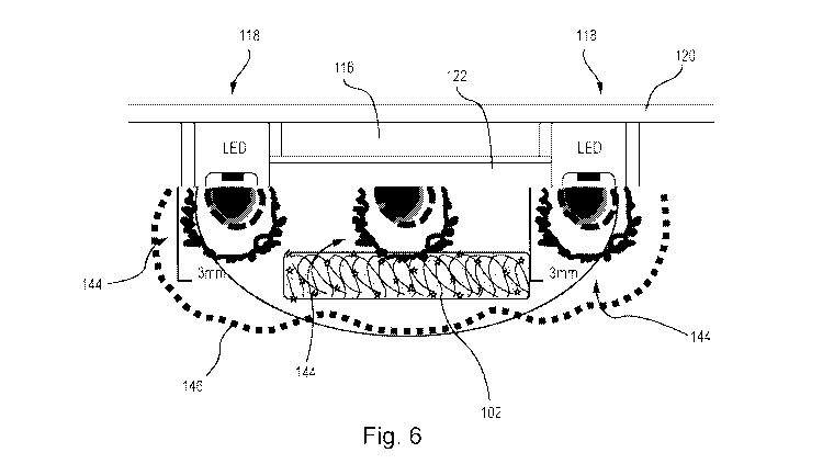
[18] Fig. 6 is a schematic diagram illustrating an advantageous manner in
which a
transcutaneous reader interacts with an implanted analyte sensor.
DETAILED DESCRIPTION
[191 As illustrated in Fig. 1, a reader 100 can be used to query an analyte
sensor 102
that is implanted within about a centimeter (e.g., a few millimeters, 2-5 rum.
1-10mm, or any
other suitable depth) beneath the surface of the skin on a user's forearm 104
(shown),
abdomen, upper arm, leg, thigh, neck, foot, etc. depending on the particular
analyte and/or
tissue site of interest. As illustrated, the reader 100 could be configured as
a patch, a wand, a
bandage, or any of a number of other form factors, which can be brought into
intimate
contact with the surface of the user's skin. -Regardless of its configuration,
the reader 100
emits into the skin excitation radiation (e.g., light) 106 of a suitable
wavelength to induce a
photo- reaction by the indicator molecules of the sensor 102, and a portion of
the light 108
emitted by the sensor 102 in response will exit from the skin. A
.photodetector within the
reader 100 (not illustrated in Fig. 1) senses and responds to the emitted
light 108 and sends a
signal 110, such as a wireless signal, to a compute device such as a tablet
computer or
smartphone 112 running an app, or a desktop computer 114 running a full
program. The
compute device can be operable to queiy the reader 100, receive signals from
the reader
indicating a concentration of the analyte, and/or receive signals indicative
of radiation
detected by the photodetector. The compute device can calculate a
concentration of an
analyte based on a signal received by the photodetector and/or track the
particular analyte.
The amount, intensity, and/or decay properties of the emitted light 108 sensed
by the
photodetector corresponds to and can be used to determine the concentration of
the analyte of
interest, as explained in more detail below. Processing of the response signal
can be
performed onboard the reader 100 or by the external device 112 or 114.
[201 As illustrated in Figs. 2-5, a reader 100 includes a photodetector 116
and a
distributed source of excitation radiation (e.g., light) 118, which are can he
mounted on a
printed circuit board 120 or any other suitable substrate. The distributed
source of excitation
radiation 118 at least partially surrounds the photodetector 116. The
photodetector 116 is
essentially centered within the distributed source of excitation radiation
118. The distributed
source of radiation 118 can include two or more LEDs, which can emit light at
a wavelength
that enables the light to penetrate through skin to the depth at which the
sensor 102 is
implanted. When the sensor 102 is illuminated, it can cause a photoreaction or
excitationlemission condition by the indicator molecules on or within the
sensor 102. For
- 6 -
CA 02990873 2017-12-22
WO 2016/210415
PCT/US2016/039566
example, as best illustrated in Fig. 2, the distributed source of radiation
118 may be
implemented with four "Super Red" LEDs, which are available from Vishay
Intertechnology
and emit light at 630 nun and which are evenly spaced from each other and
distributed evenly
around the photodetector 116, i.e., 900 apart from each other as centered on
the photodetector
116. As for the photodetector 116, it suitably may be a silicon
photomultiplier (SiPM) of the
sort available from SensL, with an active area of 3 square millimeters. Any
other suitable
source of radiation and/or detector could also be used.
[21] Suitably, the reader 100 further includes an optical band-pass filter 122
disposed
over the active, light-receiving surface of the photodetector 116, which band-
pass filter 122
allows light emitted by the sensor 102 to pass through to the photodetector
116 while
screening out "stray" light emitted by the distributed source of radiation
1.18. The band-pass
filter 122 may be constructed as a laminate using Schott RG715 colloidally
colored glass
(pass-through wavelength of approximately 715 nun and above) and Lee HT090
color filter
film (pass-through wavelengths between approximately 450 nm and 575 urn)
joined together
with Epotek 301-2 optical epoxy.
[22] The photodetector 116, distributed sources of radiation 118, and optical
band-pass
filter 122 suitably are surrounded by a substantially reflective optical
isolation ring 124,
which serves to contain light emitted by the distributed source of radiation
118 and better
concentrate it toward the sensor implant 102, as illustrated in Fig. 4.
(Figure 4 does not
depict any scattering of light as it passes into/through the skin, which is
addressed below.)
The optical isolation ring 124 is suitably formed from dark gray or black PVC
(or other
material) and may have its inner surface smoothed or coated with reflective
material to
enhance the reflection/light-concentrating benefit of the isolation ring 124.
After being
mounted to the printed circuit board 120 and having the optical isolation ring
124 installed
around them, the photodetector 116 and distributed source of radiation 118 may
be partially
encapsulated with black potting compound or, e.g., as available from MC
Electronics, but
with encapsulation leaving the light-emission points of the distributed source
of radiation 118
and the light-receiving, active surface of the photodetector 116 exposed so as
to emit and
receive radiation (light), respectively. The potting compound (or other
suitable material) can
be operable to optically isolate the distributed source of radiation 118 from
the photodetector
116, for example, preventing light from leaking from the distributed source of
radiation 118
to the photodetector 116 without the light first passing through the tissue.
[23] In some instances, each of the distributed source of radiation 11.8 can
be
configured to produce light with a particular far-field emission pattern. For
example, each of
- 7 -
CA 02990873 2017-12-22
WO 2016/210415
PCT/US2016/039566
the distributed sources of radiation 118 can produce an orb, lobe, or cone of
light such that
each distributed source of radiation 118 is configured to illuminate a
paxticular cross-
sectional area at a particular depth, in the absence of scattering and/or
reflection, in some
embodiments, each distributed source of radiation 118 may have a far-field
emission pattern
at a depth at which the implant is implanted (e.g., implantation depth, which
can be
approximately 2-5 mm) that is smaller than the implant. Similarly stated., in
some
embodiments, in the absence of scattering or reflection, no single emission
source may have
a cross sectional area and/or characteristic length at the implantation depth
sufficient to
illuminate an entirety of the implant. Moreover, as described herein, in some
embodiments
the distributed sources of radiation 118 may not be disposed directly over the
sensor. Thus,
in some embodiments, in the absence of scattering or reflection, the far-field
emission pattern
from each emission source need not be centered on the implant. In the presence
of scatter,
for example, induced by the tissue and/or reflectance e.g., from the optical
isolation ring 124,
the far-field emission patterns from the distributed sources of radiation 118
may merge into a
photon cloud that substantially envelops the implant, for example as shown and
described
with reference to FIG. 6. The use of emitters that, in the absence of
scattering and/or
reflection produce far-field emission patterns at the implantation depth that
are not large
enough to illuminate an entirety of the sensor, that do not overlap each other
and/or do not
overlap at least in a central region, can reduce the power consumption of the
reader and/or
reduce photo-bleaching effects. Similarly stated, the distributed sources of
radiation 118, in
the absence of scattering, may produce a toroidal illumination pattern at the
implantation
depth with a darkened center (e.g., the center of the illumination patter, in
the absence of
scattering, may be at least 10%, 25%, 75% and/or any other suitable percentage
darker than a
peak brightness of the illumination pattern), Such embodiments can rely on
scattering
induced by tissue to fully illuminate the implant, which presents a contrast
to known readers,
which have typically viewed scattering as a impediment that has been
compensated for by
increasing illumination power.
[24] The reader 100 suitably includes a temperature sensor 126, to measure
skin
temperature in the vicinity of the sensor 102. Skin temperature is used to
correct calculations
for quantum yield from the luminescent sensor 102. Suitably, the temperature
sensor is
provided as a TNIP006, non-contact infrared digital temperature sensor
available from Texas
Instruments,
[25] Operation of the various electronic components is controlled by a
microprocessor
128, which is also mounted to the printed circuit board 120. Ideally, the
microprocessor 128
- 8 -
CA 02990873 2017-12-22
WO 2016/210415
PCT/US2016/039566
includes built-in or integrated wireless capability to enable wireless
transmission and receipt
of data/operating commands between the reader 100 and the monitoring device,
i.e.,
smartphone or tablet computer 112 or desktop computer 114. 'Thus, a
Simbleem4RED77101,
Bluetooth Low Energy-enabled module with built-in ARM Cortex MO
microcontroller is -the
presently preferred device for use as the microprocessor 128.
[261 'The overall arrangement and interconnection of the various elechicai
components
is illustrated schematically in Fig. 5. in addition to the components
identified above, the
reader circuity includes drivers 130, which control output of the distributed
source of
radiation 118. For example, the output may be regulated in steps, from 1
milliwatt to 1.5
milliwatt to 2 milliwatt to 2.5 milliwatt total output from the four LEDs
comprising the
distributed source of radiation 118. A bias-voltage control circuit .132
boosts power-supply
voltage from the device power-supply circuit 134 to 27 volts for the
photodetector 116
(which, as noted above, is suitably a photomultiplier) to use in generating
photon-indicating
signals. The power-supply circuit 134 is configured to operate with a source
of DC voltage,
e.g., a 3-volt coin-cell (or other) battery. Analog-to-digital converter 136
digitizes the output
signal from the photodetector 116 for processing by the microprocessor 128,
and real-time
clock 138 provides date- and time-tracking functionality. EEPROM 140 provides
storage for
code, tracking of data, etc., and status indicator 142, which may be a simple
LED, is
configured to inform a user of the operational status of the device.
[271 In some instances, a reader can interact with an implanted analyte sensor
as shown
schematically in Fig. 6. in general, it is known that light entering the skin
will be scattered
quickly (i.e., within a short distance from the surface) and be diffused
within the skin. As a
result, some known readers use a discrete source of excitation radiation to
generate a small,
highly localized "orb" of radiation within the skin, and that "orb" of
radiation will only
stimulate a small portion of the embedded sensor. Therefore, because only a
percentage of
the indicator molecules on the sensor will be stimulated by radiation at any
given moment in
time, it becomes necessary with such known readers to emit radiation for a
longer period of
time or to subject the sensor to more pulse-read cycles in order to obtain a
sufficiently
accurate read through large multi-sample-averaging of readings to obtain a
meaningful
measurement of analyst concentration. However, the indicator molecule
population will
gradually and eventually lose their ability to respond to stimulating
radiation. with continued
exposure to radiation (photo-bleaching); when enough indicator molecules have
lost -their
ability to respond that the sensor is no longer able to emit a photo-signal of
sufficient signal-
to-noise ratio that is strong enough to be discernible by the photodetector
within the reader,
- 9 -
CA 02990873 2017-12-22
WO 2016/210415
PCT/US2016/039566
the analyte sensor will have lost its useful life. Therefore, the need to emit
stimulating
radiation for longer periods of time thus causing longer periods of light
exposure for the
indicator molecules ¨ associated with some known. readers is detrimental to
the longevity of
the analyte sensors they are configured to "read."
[281 Further still, with some known readers, only a portion of the analyte
sensor is able
to be read because the discrete source of radiation and the photodetector are
located side-by-
side on their supporting circuit hoard or within the overall optical assembly.
As a result of
this configuration, these two components cannot simultaneously be brought into
their
respective optimal positions with respect to an implanted analyte sensor, and
only a portion
of the sensor will be stimulated by the excitation radiation and only a
portion of the emitted
response radiation will be detected. Therefore, to overcome this situation
(which leads to
sub-optimal signal-to-noise ratios in the light being sensed/detected by the
reader), the
radiation SOW-CC in known readers tends to be significantly overpowered, e.g.,
to put out as
much as 200 milliwatts of illumination power. And that, in turn, can
substantially reduce the
useful life of the reader's batteries andlor charge intervals (in addition to
reducing the
longevity of the sensor, as noted above).
[291 In contrast, a reader 100 has a distributed source of radiation 118,
which at least
partially surrounds the photodetector 116 and which is centered with respect
to the
photodetector 116. As a result, even in an embodiment such as the disclosed
embodiment in
µvhich the distributed source of radiation 118 is formed from multiple
individual sources of
radiation (e.g., LEDs), the "orbs" of light 144 generated within the skin in
the vicinity of
each individual source will, due to scattering of light within the skin, merge
into a photon
"cloud" 146 that substantially envelopes the sensor 102, as illustrated in
Fig. 6. And this, in
turn, is advantageous for a number of reasons.
1301 First, because the sensor 102 is substantially enveloped by the photon
cloud 146,
the indicator molecules over the entirety of the sensor 102 will participate
in the analyte-
concentration-indicating process. This significantly improves signal-to-noise
ratio of the
detected photo signal. Furthermore, because more indicator molecules
participate in the
process at any given moment in time, the sensor does not need to be stimulated
for as long a
period of time as is the case with known readers; as a result, the indicator
molecules will not
be photobleached nearly as quickly as is the case with respect to the known.
readers. Further
still, because more indicator molecules participate in the process, and
because the source of
radiation is distributed relative to the sensor 102, the individual sources
(i.e., the LEDs) do
-10 -
CA 02990873 2017-12-22
WO 2016/210415
PCT/US2016/039566
not need to be driven to put out light at as high a power level as is the case
with respect to
known readers.
pi] Moreover, providing the source of radiation M distributed fashion
facilitates
centering the photodetector immediately over the sensor, where the
photodetector can sense
emitted response light as maximally as possible. Hence, in this way, too, the
configuration of
readers described herein can optimize sensitivity of the reader and accuracy
of the readings
taken with it,
[32] The foregoing disclosure is intended to be by way of example only.
Various
modifications to and departures from the disclosed embodiment may occur to
those having
skill in the art without departing from the inventive concepts disclosed
herein.
[331 In one example, a reader in accordance can be configured to read tissue
oxygen
from a Wisniewski-type implant, µyhich has been fabricated with an oxygen-
sensitive
indicator element where luminescent lifetime of the indicator is modulated by
ambient tissue
oxygen levels. In operation, synchronously pulsing the excitation array (i.e.,
the distributed
source of radiation) results in a corresponding luminescent emission return
pulse from the
implant, with a signal-amplitude decay on the trailing edge of the pulse that
is influenced
quantitatively by the luminescent lifetime of the indicator. One method of
signal processing
suited for this application is commonly known as Time Domain, the definition
of which is
the time it takes for a step response such as a pulse to decrease in value to
lie (-36.8%) of its
initial value (lo). Ratiometric signal-processing may also be used, where two
channels are
taken as a ratio with one being analyte-sensitive and the other not being
analyte-sensitive for
intensity-type (i.e., very-short-decay-time) indicator molecules.
[34] Moreover, in some embodiments, the reader can be configured in various
ways for
different applications consistent with tissue-integrating implants or non-
tissue-integrating
photo-luminescent implants. For example, the device can be configured to
operate at
multiple excitation and/or emission wavelengths. More LEDs can be included in
the
surrounding array, and each wavelength can be selected individually or in
combinations from
the system electronics controller. LEDs may be single- or multi-color type
constructs; SMT
type; die; multi-die; or combinations. LEDs may be discrete within the array,
or they may be
configured through use of a transmissive waveguide into a ring type structure
surrounding
the detector for seamless distribution. Similarly, the detector can be a
single-channel device
or it may be divided into a multi-channel detector pair or quad (or smaller)
with individual
pass filters installed onto each detector segment. The photodetector can be a
silicon
photomultiplier chip (preferred) or a photodiode, a PIN diode, an avalanche
photodiode, or
-11-
CA 02990873 2017-12-22
WO 2016/210415
PCT/US2016/039566
any optical chip-based configuration. Optical filters may be high-pass, band-
pass, thick- or
thin-film, inorganic, organic constructs, or combinations thereof, and may be
fabricated and
installed by use of adhesives, sputtering, vacuum deposition, or combinations
of these. It is
also envisioned that the readers described herein can further be configured
into pairs or more
to create additional channels for even more analytes to be read
simultaneously.
- 12 -