Note: Descriptions are shown in the official language in which they were submitted.
CA 02991339 2018-01-04
WO 2017/005289
PCT/EP2015/065356
1
A METHOD OF BUILDING AN INSULATION SYSTEM AROUND A
NAKED CONDUCTOR SECTION OF A POWER CABLE
TECHNICAL FIELD
The present disclosure generally relates to power cables. In particular, it
relates to a method of building an insulation system around a naked
conductor section of a power cable.
BACKGROUND
Today high voltage (HV) cables are typically made of cross-linked
to polyethylene (XLPE). Cross-linking can be achieved by the addition of
low
amounts of dicumyl peroxide (DCP) in a low density polyethylene (LDPE)
base material.
Factory, sea or flexible HV power cable joints are normally manufactured
using cross-linkable tapes wound around the conductor in several layers.
These layers may consist of an innermost layer that may be made of a
semiconducting material, an insulating layer arranged around the
semiconducting layer, and an outermost layer also made of a semiconducting
material. The insulating layer may for example be made of XLPE and the
semiconducting layers may be made of carbon-black filled XLPE. The tapes
are manually lapped between the two cable ends of the tapered insulation of
the two cables that are to be jointed. Each of these three layers is then
cured
under heat and pressure in a separate step so that the tapes melt together
forming a homogeneous material without any voids.
The tapes used for the insulation system of the factory joints and the factory
joints as such are manufactured in the cable factory under strict cleanness
conditions. The same applies also in case the insulation system of a defected
power cable is to be restored. The manual jointing or restoration procedure is
lengthy and vulnerable to contamination. It may require up to four days, or
more, of manufacturing time, including the required crosslinking process, in
three shift work schedule. Moreover, a person performing the
CA 02991339 2018-01-04
WO 2017/005289
PCT/EP2015/065356
2
jointing/restoration procedure must be trained for several years before being
authorised to perform the jointing. Furthermore, additional time is essential
for heat treatment in order to degas polar by-products of the crosslinking
reaction, known to impair the insulation's performance. The latter process
can last from few days up to weeks.
SUMMARY
In view of the above, an object of the present disclosure is to solve, or at
least
mitigate, the problems of the prior art.
Hence, according to a first aspect of the present disclosure there is provided
a
method of building an insulation system around a naked conductor section of
a power cable, which power cable has a conductor which includes the naked
conductor section and which power cable comprises an insulation system
already provided around a majority of the conductor, which insulation system
comprises an inner semiconducting layer arranged around the conductor, an
insulation layer arranged around the inner semiconducting layer, and an
outer semiconducting layer arranged around the insulation layer, and
wherein the method comprises: a) placing the naked conductor section in a
mould, and b) moulding an insulation system around the naked conductor
section, wherein the moulding of the insulation system involves injecting a
first semiconducting compound into a first mould cavity to form an inner
semiconducting layer around the naked conductor section, injecting an
insulation compound into a second mould cavity to form an insulation layer
around the inner semiconducting layer, and injecting a second
semiconducting compound into a third mould cavity to form an outer
semiconducting layer around the insulation layer.
An effect obtainable thereby is that of reduced manufacturing and heat
treatment time/costs. By utilising injection moulding it is anticipated that
the
manufacturing time of the insulation system may be reduced with up to 40%,
mainly resulting from the absence of long vulcanization steps, and in addition
eliminate fully any time spent for heat treatment in a degassing free cable
system.
CA 02991339 2018-01-04
WO 2017/005289
PCT/EP2015/065356
3
Additional advantages include no costs for the production of semiconducting
layer tapes and insulating layer tapes, as no tapes are needed. Furthermore,
the production quality can be kept more constant e.g. due to less operator
dependent process. This results in improved performance and reliability
because of fewer voids and defects, better interfaces and a cleaner
manufacturing process.
According to one embodiment step a) comprises placing the naked conductor
section in a first mould insert in the mould, the first mould insert forming
the
first mould cavity and having a first inner diameter.
According to one embodiment step a) further comprises placing a first sealing
ring around the insulation system to seal the first mould insert at one end
thereof and placing a second sealing ring around the insulation system to seal
the first mould insert at the other end thereof.
According to one embodiment step b) comprises bi) injecting the first
semiconducting compound into the first mould insert, thereby providing the
inner semiconducting layer around the naked conductor section, and thus
forming a section provided with an inner semiconducting layer, b2) removing
the first mould insert from the mould and placing a second mould insert with
a second inner diameter that is larger than the first inner diameter into the
mould, the second mould insert forming the second mould cavity, b3) placing
the joint section provided with the inner semiconducting layer in the second
mould insert, b4) injecting the insulation compound into the second mould
insert, thereby providing the insulation layer around the inner
semiconducting layer of the section provided with the inner semiconducting
layer, and thus forming a section provided with an insulation layer, b5)
removing the second mould insert from the mould and placing a third mould
insert with a third inner diameter that is larger than the second inner
diameter into the mould, the third mould insert forming the third mould
cavity, b6) placing the section provided with the insulation layer in the
third
mould insert, and b7) injecting the second semiconducting compound into
CA 02991339 2018-01-04
WO 2017/005289
PCT/EP2015/065356
4
the third mould insert, thereby providing the outer semiconducting layer
around the insulation layer of the section provided with the insulation layer.
By utilising several mould inserts, one for each layer to be moulded the costs
may be lowered because one mould may be used for all the layers. Moreover,
the utilisation of a single mould with mould inserts reduces manufacturing
time as there is no need to replace the entire mould for each layer.
According to one embodiment step b3) further comprises placing a third
sealing ring around the insulation system to seal the second mould insert at
one end thereof and placing a fourth sealing ring around the insulation
system to seal the second mould insert at the other end thereof.
According to one embodiment step b6) further comprises placing a fifth
sealing ring around the insulation system to seal the third mould insert at
one
end thereof and placing a sixth sealing ring around the insulation system to
seal the third mould insert at the other end thereof.
By selecting suitable dimensions of the sealing rings any plastic deformation
of the cable may be avoided. Any plastic deformation of the insulation layer
and semiconducting layers would negatively affect electrical performance
inducing local field enhancements.
According to one embodiment each of the first sealing ring, second sealing
ring, third sealing ring, fourth sealing ring, fifth sealing ring, and sixth
sealing ring are made of metal.
According to one embodiment the mould comprises a ring-shaped runner
system having a ring-shaped runner which in the beginning of each mould
cycle only has a single gate opening, which single gate opening is located
opposite to a sprue.
According to one embodiment the mould comprises a movable sleeve
arranged in a first position at the beginning of each mould cycle thereby
forming the single gate opening, wherein the method comprises moving the
sleeve axially from the first position to a second position to obtain a gate
CA 02991339 2018-01-04
WO 2017/005289
PCT/EP2015/065356
along the entire circumference of the ring-shaped runner, wherein the sleeve
is moved from the first position to the second position when any of the first
semiconducting compound, the insulation compound and the second
semiconducting compound has reached the single gate opening.
5 Thereby uniform filling of the cavity may be obtained. Conventional
runner
systems would lead to a non-balanced filling of the cavity which potentially
can cause issues of eccentricity of the conductor, which in turn leads to
detrimental electrical performance. The ring-shaped runner system
furthermore reduces the risk of obtaining pronounced weld-line(s), which
to potentially can affect negatively electrical and mechanical performance
of the
jointed power cable. Furthermore, due to the semi-open gate structure of the
ring-shaped runner system, any air may be pressed into the mould cavity
during moulding, resulting from the ring-shaped runner being filled with an
injected compound. Thereby any air trap/diesel effect problems in the ring-
shaped runner may be avoided.
This ring-shaped runner system may be utilised when moulding all three
layers, i.e. the inner semiconducting layer, the insulation layer and the
outer
semiconducting layer. Each mould insert may for example be provided with a
respective ring-shaped runner system for this purpose.
According to one embodiment the mould comprises a sensor arranged to
sense one of pressure and temperature to determine whether one of the first
semiconducting compound, the insulation compound and the second
semiconducting compound has reached the single gate opening after having
been injected into the ring-shaped runner.
According to one embodiment the power cable is a high voltage power cable.
According to one embodiment each of the first semiconducting compound
and the second semiconducting compound comprises a thermoplastic
material filled with semiconducting or conductive inclusions and the
insulation compound is a thermoplastic material.
CA 02991339 2018-01-04
WO 2017/005289
PCT/EP2015/065356
6
According to one embodiment the power cable is a first power cable wherein
the conductor is a first conductor having a first naked conductor section,
wherein the method comprises, prior to step a), jointing the first naked
conductor section with a second naked conductor section of a second power
cable to obtain the naked conductor section, which second power cable has a
second conductor and inner semiconducting layer arranged around the
second conductor, an insulation layer arranged around the inner
semiconducting layer, and an outer semiconducting layer arranged around
the insulation layer.
to According to a second aspect of the present disclosure there is provided
a
power cable obtainable by the method according to the first aspect presented
herein.
Generally, all terms used in the claims are to be interpreted according to
their
ordinary meaning in the technical field, unless explicitly defined otherwise
herein. All references to "a/an/the element, apparatus, component, means",
etc. are to be interpreted openly as referring to at least one instance of the
element, apparatus, component, means, etc., unless explicitly stated
otherwise.
BRIEF DESCRIPTION OF THE DRAWINGS
The specific embodiments of the inventive concept will now be described, by
way of example, with reference to the accompanying drawings, in which:
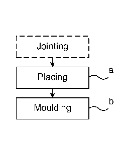
Fig. 1 is a flowchart of a method of building an insulation system around a
naked conductor section of a power cable;
Fig. 2 is a flowchart of a variation of the method depicted in Fig. 1;
Fig. 3 is a schematic view of an example of an arrangement utilised for
manufacturing an insulation system by means of moulding in accordance
with the methods of Figs 1 and 2;
Fig. 4 shows a top view of two halves of an example of a sealing ring; and
CA 02991339 2018-01-04
WO 2017/005289
PCT/EP2015/065356
7
Fig. 5a shows a sectional view of an example of a ring-shaped runner system;
Figs 5b and 5c show perspective views of the ring-shaped runner system in
Fig. 5a; and
Figs 6a-6d shows schematic perspective views of a second example of a ring-
shaped runner system during a mould cycle.
DETAILED DESCRIPTION
The inventive concept will now be described more fully hereinafter with
reference to the accompanying drawings, in which exemplifying
embodiments are shown. The inventive concept may, however, be embodied
to in many different forms and should not be construed as limited to the
embodiments set forth herein; rather, these embodiments are provided by
way of example so that this disclosure will be thorough and complete, and
will fully convey the scope of the inventive concept to those skilled in the
art.
Like numbers refer to like elements throughout the description.
The present disclosure relates to a method of building, or completing, an
insulation system around a naked conductor section of a power cable, which
power cable already has an existing insulation system arranged around the
majority of the conductor of the power cable. The insulation system that is
built around the naked conductor section is built by means of moulding an
inner semiconducting layer around the naked conductor section of the power
cable, by moulding an insulation layer around the inner semiconducting
layer, and by moulding an outer semiconducting layer around the insulation
layer. The building may involve the restoration of the insulation system of a
power cable which has an insulation system with manufacturing defects, or it
may involve the jointing of a first power cable and a second power cable thus
forming a power cable, in which case an insulation system is built around the
naked conductor section, which includes the joint between the two jointed
conductors of the first power cable and the second power cable. This type of
insulation system building is normally performed in the factory as the
CA 02991339 2018-01-04
WO 2017/005289
PCT/EP2015/065356
8
restoration requires high degrees of cleanness in order not to introduce
impurities into the insulation system.
The power cable may be a high voltage power cable. The power cable may be
an alternating current (AC) power cable having a plurality of cores, namely
one for each electrical phase, in which case each core may be jointed
according to the methods described herein, or a direct current (DC) power
cable.
A first example of building an insulation system around a naked conductor
section of a power cable will now be described. In this example, the building
involves building or manufacturing an insulation system of a jointed first
power cable and second power cable.
As shown in Fig. 3, the first power cable Ci comprises a first conductor 4a,
and a first insulation system comprising an inner semiconducting layer 4h
arranged around the first conductor 4a, an insulation layer 4c arranged
around the inner semiconducting layer 4h and an outer semiconducting layer
4d arranged around the insulation layer 4c.
Similarly to the first power cable Ci, the second power cable comprises a
second conductor, and a second insulation system comprising an inner
semiconducting layer arranged around the second conductor, an insulation
layer arranged around the inner semiconducting layer and an outer
semiconducting layer arranged around the insulation layer.
In order to prepare for the jointing disclosed herein, the first insulation
system normally has a tapering section, which tapers towards a naked end
section of the first conductor. Similarly, the second insulation system
normally has a tapering section, which tapers towards a naked end section of
the first conductor.
By means of the methods presented herein, each of the first insulation system
and the second insulation system may be restored so that when the naked
end section of the first conductor and the naked end section of the second
CA 02991339 2018-01-04
WO 2017/005289
PCT/EP2015/065356
9
conductor have been jointed, a single integrated insulation system may be
obtained. The jointing disclosed herein replaces current jointing solutions
utilising several layers of tapes wound around the jointed conductors of the
first power cable and the second power cable to restore the insulation system
thereof.
In order to joint the first power cable with the second power cable, it is
assured that the first conductor has a naked end section, without the first
insulation system. This may be obtained either by not providing any first
insulation system to this part of the first conductor in the first place, or
the
first insulation system may be removed from this section of the first power
cable for the purpose of jointing. The first insulation system may taper
towards the naked end section of the first conductor.
Furthermore, the second conductor has a naked end section, without the
second insulation system. This may be obtained either by not providing any
second insulation system to this part of the second conductor in the first
place, or the second insulation system may be removed from this section of
the second power cable for the purpose of jointing. The second insulation
system may taper towards the naked end section of the second conductor.
With reference to Fig. 1, a general method of jointing a first power cable
with
a second power cable will now be described.
The naked end section of the first conductor and the naked end section of the
second conductor are jointed thus forming a naked conductor section. This
jointing is normally performed by thermal joining, for example by means of
welding.
In a step a) the naked conductor section is placed in a mould.
In a step b) an insulation system is moulded around the naked conductor
section. The moulding of the insulation system involves injecting a first
semiconducting compound into a first mould cavity to form an inner
semiconducting layer around the naked conductor section, injecting an
CA 02991339 2018-01-04
WO 2017/005289
PCT/EP2015/065356
insulation compound into a second mould cavity to form an insulation layer
around the inner semiconducting layer, and injecting a second
semiconducting compound into a third mould cavity to form an outer
semiconducting layer around the insulation layer.
5 Step b) of moulding may involve utilising several moulds, one for each
layer.
Alternatively several mould inserts may be used; one for each layer. For each
layer that is being moulded, a mould insert may be placed in the mould, thus
forming a mould cavity in which a particular layer may be moulded. By
utilising mould inserts instead of several moulds, costs may be reduced both
10 due to the costs savings of having to invest only in a single mould, and
due
the reduced time for only having to replace the interior of the mould by
means of mould inserts instead of having to replace the entire mould during
the moulding process.
Fig. 2 describes the alternative of the method utilising several mould inserts
in more detail. In the method an injection mould is used to handle over-
moulding of different types and different diameters of polymer layers. Such a
mould may include a common frame with an integrated runner system used
for all polymer layers. The common frame may also include cooling circuits
and an ejection system.
Thus, when several mould inserts are used to restore the insulation system,
one mould insert for each layer, step a) further comprises placing the naked
conductor section in a first mould insert in the mould. The first mould insert
forms a first mould cavity and has a first inner diameter. This first inner
diameter corresponds to the outer diameter of the inner semiconducting
layer.
Fig. 3 shows an arrangement 1 which includes a first power cable Ci having a
first conductor 4a and a second power cable C2 having a second conductor
6a, which are being jointed utilising mould inserts for the different layers
of
the insulation system of the jointed power cable. In particular, the
arrangement 1 includes a mould insert, for example a first mould insert 3,
CA 02991339 2018-01-04
WO 2017/005289
PCT/EP2015/065356
11
and sealing rings, for example a first sealing ring Ri, and a second sealing
ring R2. The exemplified mould insert forms a mould cavity and is similar for
all mould inserts described herein, i.e. the first mould insert, a second
mould
insert and a third mould insert, except that their inner dimensions differ
such
that different diameter layers may be moulded around each other. The
sealing rings are arranged to retain the polymer compound, e.g. a first
semiconducting compound, an insulation compound, and a second
semiconducting compound in the mould insert during moulding and to fix
the first power cable and the second power cable against the mould.
Step a) may thus further comprise placing a first sealing ring Ri around the
first insulation system to seal the first mould insert 3 at one end thereof.
Step
a) may also comprise placing a second sealing ring R2 around the second
insulation system to seal the first mould insert 3 at the other end thereof.
As
will be understood in the following, each mould insert may be associated with
respective sealing rings.
An example of a sealing ring R is shown in Fig. 4. In particular, two halves 5
and 7 are shown. The sealing ring R has a tubular portion 9 arranged to
provide a tight fit around the corresponding layer that is to be moulded. The
tubular portion 9 may thus have an inner diameter d that provides the
required tightness and may essentially correspond to the inner diameter of
the corresponding mould insert. This inner diameter d may be slightly
smaller, equal to, or slightly larger, than the inner diameter of the
corresponding mould insert. The sealing ring R furthermore has a tubular
portion ii which when the sealing ring R is in use is arranged around the
outermost semiconducting layer. The tubular portion 11 may thus have an
inner diameter D essentially corresponding to the outer diameter of the first
power cable and the outer diameter of the second power cable.. The outer
diameter of the first power cable and the second power cable is generally the
same. Here, with the outer diameter of the first power cable/second power
cable is generally meant the outer diameter of the outer semiconducting layer
of the first insulation system and the second insulation system, respectively,
of the already existing first insulation system and second insulation system.
CA 02991339 2018-01-04
WO 2017/005289
PCT/EP2015/065356
12
Typically, no outer sheath has been arranged around the first power cable
and the second power cable at this point in the manufacturing process. The
structure of the sealing ring R is identical for all sealing rings that will
be
described herein, i.e. the first sealing ring and the second sealing ring, as
well
as a third, a fourth, a fifth and a sixth sealing ring that will be described
in the
following. All of these sealing rings may for example be made of metal, or a
plastic material.
Returning to Fig. 2, step b may comprise the following steps.
In a step bi) the first semiconducting compound is injected into the first
to mould insert. The inner semiconducting layer is thereby provided around
the
naked conductor section. In this manner a joint section provided with an
inner semiconducting layer is formed.
In a step b2) the first mould insert is removed from the mould.
The sprue and runner segment formed by the first semiconducting compound
is removed using proper tools such as a knife. The surface of the inner
semiconducting layer is then smoothened e.g. by glassing and/or grinding.
Furthermore in step b2) a second mould insert with a second inner diameter
that is larger than the first inner diameter is placed into the mould. The
second mould insert forms a second mould cavity.
In a step b3) the joint section provided with the inner semiconducting layer
is
placed in the second mould insert.
Step b3) may further comprise placing the third sealing ring around the first
insulation system to seal the second mould insert at one end thereof and to
place a fourth sealing ring around the second insulation system to seal the
second mould insert at the other end thereof.
In a step b4) the insulation compound is injected into the second mould
insert. The insulation layer is thereby provided around the inner
semiconducting layer of the joint section provided with the inner
CA 02991339 2018-01-04
WO 2017/005289
PCT/EP2015/065356
13
semiconducting layer. Hence a joint section provided with an insulation layer
is formed.
In a step b5) the second mould insert is removed from the mould.
The sprue and runner segment formed by the insulation compound is
removed using proper tools such as a knife. The surface of the insulation
layer is then smoothened e.g. by glassing and/or grinding.
Furthermore in step b5) a third mould insert with a third inner diameter that
is larger than the second inner diameter is placed into the mould. The third
mould insert forms a third mould cavity.
In a step b6) the joint section provided with the insulation layer is placed
in
the third mould insert.
Step b6) may further comprise placing a fifth sealing ring around the first
insulation system to seal the third mould insert at one end thereof and to
place a sixth sealing ring around the second insulation system to seal the
third mould insert at the other end thereof.
In a step b7) the second semiconducting compound is injected into the third
mould insert. The outer semiconducting layer is thereby provided around the
insulation layer of the joint section provided with the insulation layer.
The sprue and runner segment formed by the second semiconducting
compound is removed using proper tools such as a knife. The surface of the
outer semiconducting layer is then smoothened e.g. by glassing and/or
grinding. The jointed power cable is now ready for the manufacturing of
outer layers such as shielding and moisture barrier.
Typically, the first semiconducting compound and the second
semiconducting compound are the same thermoplastic material comprising
semiconducting or conductive inclusions such as carbon black, carbon
nanotubes, graphene, or metal particles. An example of a thermoplastic
material is a polyethylene-based thermoplastic blend. The insulation
CA 02991339 2018-01-04
WO 2017/005289
PCT/EP2015/065356
14
compound is also a thermoplastic material, for example a polyethylene-based
thermoplastic blend. Another example of a material, which is not a
thermoplastic material, but which may be used for the semiconducting layers
and for the insulation layer is XLPE, which for the semiconducting layers
may include e.g. carbon black.
A second application for building an insulation system of a power cable will
now shortly be described. According to this example, the insulation system of
a power cable that has a damaged or defect insulation system is restored. The
power cable comprises a conductor, an inner semiconducting layer, an
insulation layer arranged around the inner semiconducting layer and an
outer semiconducting layer arranged around the insulation layer. The power
cable also has a naked conductor section, i.e. a section of the conductor
which
is not provided with the insulation system. The insulation system has been
removed at this section of the power cable to expose the naked conductor
section. In particular, it is this section of the power cable that originally
had
an insulation system with defects, and which is to be restored.
According to the method, this naked conductor section is provided with an
insulation system by means of layer-wise moulding of all three layers in the
same manner as has previously been described for the restoration of the
insulation system of the joint.
In order to prepare for the manufacturing of the insulation system, the
insulation system normally has a tapering section, which tapers towards a
naked conductor section. Similarly, at the other end of the naked conductor
section the insulation system normally has a tapering section, also tapering
towards the naked conductor section. Steps a) and b) are carried out in the
same manner as has been disclosed above. Moreover, steps bi)-b7) may also
optionally be performed. In this case the sealing rings are arranged around
the ends of the insulation system and over the tapering insulation system
portions so as to seal the naked conductor section, and subsequently the
layers moulded thereon.
CA 02991339 2018-01-04
WO 2017/005289
PCT/EP2015/065356
Fig. 5a shows in more detail a portion of a mould insert in section along the
central axis A of a power cable, including the ring-shaped runner system 17.
The ring-shaped runner system 17 includes a ring-shaped runner 18 that
extends circumferentially 360 degrees around a mould cavity 25 and a sprue
5 19 connected to the ring-shaped runner 18. The ring-shaped runner system
17
includes an inner wall 24 which defines a circumferential gate 22 through
which the injected compound may enter the mould cavity 25. The axial
distance between inner wall 24 and a mould insert wall 20 gradually
increases in the circumferential direction from the sprue 19 to the distal end
10 of the ring-shaped runner 18 relative to the sprue 19, i.e. 180 degrees
from
the sprue 19. The gate 22 hence increases gradually along the circumference
of the ring-shaped runner 18, in a direction away from the sprue 19.
The inner wall 24, or generally the ring-shaped runner 18, may be provided
with a cut-out 26 at half a turn from the sprue 19, i.e. at 180 degrees from
15 sprue 19, to provide an opening into the mould cavity 25. The gradual
increase of the gate 22 provides uniform distribution of the polymer into the
mould cavity 25 and design of the gate 22 and the cut-out 26 increases the
packing time.
Fig. 5b shows a perspective view of a half of a mould insert thus exposing the
ring-shaped runner system 17. Fig. 5c shows a perspective view of the other
half of a mould insert exposing the ring-shaped runner system 17.
According to one variation the ring-shaped runner system 17 may further
comprises a sleeve 27 arranged around the mould cavity 25, as schematically
illustrated in Figs 6a-6d, in which a mould cycle is shown during which a
polymer P is being injected into the ring-shaped runner 18. The sleeve 27 may
for example be arranged in the mould insert. The sleeve 27 is movable along
the central axis A between a first position and a second position. At the
beginning of each mould cycle, i.e. before each of the inner semiconducting
layer, the insulation layer and the outer semiconducting layer is being
moulded, the sleeve 27 is arranged in the first position along the central
axis
A, as shown in Fig. 6a. In the first position, the sleeve 27 and the inner
wall of
CA 02991339 2018-01-04
WO 2017/005289
PCT/EP2015/065356
16
the ring-shaped runner 18 abut each other, whereby entry into the mould
cavity 25 is blocked along the entire contact surface of the ring-shaped
runner
18 and the sleeve 27. The ring-shaped runner 18 comprises a cut-out defining
a single gate opening 29 located opposite to the sprue 19, i.e. at about 180
degrees angle from the sprue 19. When the sleeve 27 is in the first position,
a
single entry point, i.e. the single gate opening 29, is provided into the
mould
cavity 25
The ring-shaped runner system 17 may further include a sensor 31 arranged
to sense at least one of a pressure and temperature in the ring-shaped runner
18. When the ring-shaped runner 18 has been filled with the injected
compound, i.e. the polymer P, and the injected compound reaches the single
gate opening 29, the sensor 31 provides a signal which triggers the sleeve 27
to move from the first position to the second position along the central axis
A,
as shown in Figs 6b-c. In the second position, the sleeve 27 has moved away
from the inner wall. In this way, a gate is created around the entire
circumference of the mould cavity 25, and the compound injected into the
ring-shaped runner 18 may enter the mould cavity 25 along the entire
circumference of the mould cavity 25. Fig. 6d shows the mould cavity 25
being filled with the polymer P.
It should be noted that other types of runner systems could be used as an
alternative to a ring-shaped runner system, for example a runner system that
provides direct injection moulding with a sprue.
The inventive concept has mainly been described above with reference to a
few examples. However, as is readily appreciated by a person skilled in the
art, other embodiments than the ones disclosed above are equally possible
within the scope of the inventive concept, as defined by the appended claims.