Note: Descriptions are shown in the official language in which they were submitted.
CA 02991933 2018-01-11
84140058
1
INTEGRATED DEVICE PACKAGE COMPRISING BRIDGE IN LITHO-
ETCHABLE LAYER
CROSS-REFERENCE TO RELATED APPLICATION
[0001] This application claims priority to and the benefit of Non-
Provisional Application
No. 14/832,363 filed in the U.S. Patent and Trademark Office on August 21,
2015.
BACKGROUND
Field
[0002] Various features relate to an integrated device package that
includes a bridge in a
litho-etchable layer.
Background
[0003] FIG. 1 illustrates an integrated device package 100 that includes
a first die 102, a
second die 104, and a package substrate 106. The package substrate 106
includes a dielectric
layer and a plurality of interconnects 110. The package substrate 106 is a
laminated substrate.
The plurality of interconnects 110 includes traces, pads and/or vias. The
first die 102 is
coupled to the package substrate 106 through the first set of solder balls
112. The second die
104 is coupled to the package substrate 106 through the second set of solder
balls 114. The
package substrate 106 is coupled to a printed circuit board (PCB) 108 through
the third set of
solder balls 116. FIG. 1 illustrates that the first die 102 is coupled to the
second die 104
through the first set of solder balls 112, interconnects from the plurality of
interconnects 110,
and the second set of solder balls 114.
[0004] One drawback of the integrated device package 100 shown in FIG. 1
is that it
creates an integrated device package with a form factor that may be too large
for the needs of
mobile computing devices and/or wearable computing devices. This may result in
a package
that is either too large and/or too thick. That is, the integrated device
package configuration
shown in FIG. 1 may be too thick and/or have a surface area that is too large
to meet the needs
and/or requirements of mobile computing devices and/or wearable computing
devices.
84140058
2
[0005] Another drawback of the integrated device package 100 is that the
configuration of
the plurality of interconnects 110 does not provide high density interconnects
between the first
die 102 and the second die 104. This greatly limits the number of
interconnects that can exist
between the first die 102 and the second die 104, therefore limiting the
communication
bandwidth between the first die 102 and the second die 104.
[0006] Therefore, there is a need for an integrated device package that
includes high density
interconnects between dies. Ideally, such an integrated device package will
have a better form
factor, provide an improved power distribution network (e.g., improved power
routing to and
from dies), while at the same time meeting the needs and/or requirements of
mobile computing
devices and/or wearable computing devices.
SUMMARY
[0007] Various features relate to an integrated device package that
includes a bridge in a
litho-etchable layer.
[0008] A first example provides an integrated device package base
comprising: an
encapsulation portion comprising: an encapsulation layer; a bridge, at least
partially embedded
in the encapsulation layer, configured to provide a first electrical path for
a first signal between
a first die and a second die; and a first via, in the encapsulation layer,
coupled to the bridge,
wherein the first via and the bridge are configured to provide a second
electrical path for a
second signal to the first die; and a redistribution portion coupled to the
encapsulation portion,
the redistribution portion comprising: at least one dielectric layer; and at
least one interconnect,
in the at least one dielectric layer, coupled to the first via, wherein the
bridge comprises: a
substrate; a dielectric layer; a first set of interconnects configured to
provide the first electrical
path for the first signal between the first die and the second die; and a
through substrate via
(TSV) traversing at least the substrate, the TSV coupled to the first via, the
TSV configured to
provide the second electrical path for the second signal to the first die.
[0009] A second example provides an integrated device package base
comprising: an
encapsulation portion comprising: an encapsulation layer; means, at least
partially embedded in
the encapsulation layer, for providing a first electrical path for a first
signal between a first die
and a second die; and a first via, in the encapsulation layer, coupled to the
means for providing
the first electrical path for the first signal between the first die and the
second die, wherein the
Date Recue/Date Received 2022-09-14
84140058
3
first via and the means for providing the first electrical path for the first
signal between the first
die and the second die, are configured to provide a second electrical path for
a second signal to
the first die; and a redistribution portion coupled to the encapsulation
portion, the redistribution
portion comprising: at least one dielectric layer; and at least one
interconnect, in the at least one
dielectric layer, coupled to the first via, wherein the means for providing
the first electrical path
for the first signal between the first die and the second die comprises: a
substrate; a dielectric
layer; a first set of interconnects configured to provide the first electrical
path for the first signal
between the first die and the second die; and a through substrate via (TSV)
traversing at least
the substrate, the TSV coupled to the first via, the TSV configured to provide
the second
electrical path for the second signal to the first die.
[00101 A third example provides an integrated device package comprising: a
first die; a
second die; and a base coupled to the first die and the second die,
comprising: an encapsulation
portion coupled to the first die and the second die, comprising: an
encapsulation layer; a bridge,
at least partially embedded in the encapsulation layer, configured to provide
a first electrical
path for a first signal between the first die and the second die; and a first
via, in the encapsulation
layer, coupled to the bridge, wherein the first via and the bridge are
configured to provide a
second electrical path for a second signal to the first die; and a
redistribution portion coupled to
the encapsulation portion, the redistribution portion comprising: at least one
dielectric layer;
and at least one interconnect, in the at least one dielectric layer, coupled
to the first via; wherein
the bridge comprises: a substrate; a dielectric layer; a first set of
interconnects configured to
provide the first electrical path for the first signal between the first die
and the second die; and
a through substrate via (TSV) traversing at least the substrate, the TSV
coupled to the first via,
the TSV configured to provide the second electrical path for the second signal
to the first die.
[00111 A fourth example provides an integrated device package comprising: a
first die; a
second die; and a base coupled to the first die and the second die,
comprising: an encapsulation
portion coupled to the first die and the second die, comprising: an
encapsulation layer; means,
at least partially embedded in the encapsulation layer, for providing a first
electrical path for a
first signal between the first die and the second die; and a first via, in the
encapsulation layer,
coupled to the means for providing the first electrical path for the first
signal between the first
die and the second die, wherein the first via and the means for providing the
first electrical path
Date Recue/Date Received 2022-09-14
84140058
3a
for the first signal between the first die and the second die, are configured
to provide a second
electrical path for a second signal to the first die; and a redistribution
portion coupled to the
encapsulation portion, the redistribution portion comprising: at least one
dielectric layer; and at
least one interconnect, in the at least one dielectric layer, coupled to the
first via, wherein the
means for providing the first electrical path for the first signal between the
first die and the
second die comprises: a substrate; a dielectric layer; a first set of
interconnects configured to
provide the first electrical path for the first signal between the first die
and the second die; and
a through substrate via (TSV) traversing at least the substrate, the TSV
coupled to the first via,
the TSV configured to provide the second electrical path for the second signal
to the first die.
DRAWINGS
[0012] Various features, nature and advantages may become apparent from the
detailed
description set forth below when taken in conjunction with the drawings in
which like reference
characters identify correspondingly throughout.
[0013] FIG. 1 illustrates an integrated device package comprising two dies.
[0014] FIG. 2 illustrates an example of an integrated device package
comprising a high
density interconnect bridge, with through substrate vias, in an encapsulation
layer.
Date Recue/Date Received 2022-09-14
CA 02991933 2018-01-09
WO 2017/034641
PCT/US2016/035895
4
[0015] FIG. 3 illustrates an example of an integrated device package
comprising a
high density interconnect bridge, with through substrate vias, in an
encapsulation layer.
[0016] FIG. 4 illustrates an example of a profile view of a high density
interconnect
bridge with through substrate vias (TSVs).
[0017] FIG. 5 illustrates an example of a plan view of a high density
interconnect
bridge with through substrate vias (TSVs).
[0018] FIG. 6 illustrates an example of a profile view of an integrated
device
package base comprising a high density interconnect bridge, with through
substrate
vias, in an encapsulation layer.
[0019] FIG. 7 illustrates another example of a profile view of an
integrated device
package base comprising a high density interconnect bridge, with through
substrate
vias, in an encapsulation layer.
[0020] FIG. 8 illustrates an example of a profile view of an integrated
device
package base comprising a high density interconnect bridge, with through
substrate
vias, in an encapsulation layer.
[0021] FIG. 9 illustrates another example of a profile view of an
integrated device
package base comprising a high density interconnect bridge, with through
substrate
vias, in an encapsulation layer.
[0022] FIG. 10 illustrates an example of a profile view of an integrated
device
package comprising a high density interconnect bridge, with through substrate
vias, in
an encapsulation layer.
[0023] FIG. 11 illustrates an exemplary sequence for providing /
fabricating a high
density interconnect bridge with through substrate vias (TSVs).
[0024] FIG. 12 illustrates an exemplary flow diagram of a method for
providing
fabricating a high density interconnect bridge with through substrate vias
(TSVs).
[0025] FIG. 13 (comprising FIGS. 13A-13C) illustrates an exemplary
sequence for
providing / fabricating an integrated device package comprising a high density
bridge,
with through substrate vias (TSVs), in an encapsulation layer.
[0026] FIG. 14 illustrates an exemplary flow diagram of a method for
providing /
fabricating an integrated device package comprising a high density bridge,
with through
substrate vias (TSVs), in an encapsulation layer.
[0027] FIG. 15 illustrates an example of a semi-additive patterning (SAP)
process.
[0028] FIG. 16 illustrates an example of flow diagram of a semi-additive
patterning
(SAP) process.
CA 02991933 2018-01-09
WO 2017/034641
PCT/US2016/035895
[0029] FIG. 17 illustrates an example of a damascene process.
[0030] FIG. 18 illustrates an example of a flow diagram of a damascene
process.
[0031] FIG. 19 illustrates various electronic devices that may integrate
an integrated
device package, a semiconductor device, a die, an integrated circuit and/or
PCB
described herein.
DETAILED DESCRIPTION
[0032] In the following description, specific details are given to provide
a thorough
understanding of the various aspects of the disclosure. However, it will be
understood
by one of ordinary skill in the art that the aspects may be practiced without
these
specific details. For example, circuits may be shown in block diagrams in
order to avoid
obscuring the aspects in unnecessary detail. In other instances, well-known
circuits,
structures and techniques may not be shown in detail in order not to obscure
the aspects
of the disclosure.
Overview
100331 Some features pertain an integrated device package that includes a
first die, a
second die, and a base (e.g., integrated device package base) coupled to the
first die and
the second die. The base includes an encapsulation portion and a
redistribution portion
coupled to the encapsulation portion. The encapsulation portion is coupled to
the first
die and the second die. The encapsulation portion includes an encapsulation
layer, a
bridge, and a first via. The encapsulation layer may be a litho-etchable
material (e.g.,
material etchable by photolithography process). The bridge is at least
partially
embedded in the encapsulation layer. The bridge is configured to provide a
first
electrical path for a first signal (e.g., input/output signal) between the
first die and the
second die. The first via is in the encapsulation layer. The first via is
coupled to the
bridge. The first via and the bridge are configured to provide a second
electrical path for
a second signal (e.g., power signal, ground reference signal) to the first
die. In some
implementations, the first via has a profile cross section comprising a V
shape or a U
shape. The redistribution portion includes at least one dielectric layer, and
at least one
interconnect in the at least one dielectric layer. The at least one
interconnect is coupled
to the first via. In some implementations, the bridge includes a substrate, a
dielectric
layer, a first set of interconnects configured to provide the first electrical
path for the
first signal between the first die and the second die. The bridge also
includes a through
CA 02991933 2018-01-09
WO 2017/034641
PCT/US2016/035895
6
substrate via (TSV) traversing at least the substrate. The TSV is coupled to
the first via.
The TSV is configured to provide the second electrical path for the second
signal to the
first die. In some implementations, the TSV traverses the substrate and the
dielectric
layer of the bridge.
[0034] An
interconnect is an element or component of a device (e.g., integrated
device, integrated device package, die) and/or a base (e.g., integrated device
package
base, package substrate, printed circuit board, interposer) that allows or
facilitates an
electrical connection between two points, elements and/or components. In some
implementations, an interconnect may include a trace, a via, a pad, a pillar,
a
redistribution metal layer, and/or an under bump metallization (UBM) layer. In
some
implementations, an interconnect is an electrically conductive material that
provides an
electrical path for a signal (e.g., data signal, ground signal, power signal).
An
interconnect may include more than one element / component. A set of
interconnects
may include one or more interconnects.
[0035] A
redistribution layer or a redistribution metal layer is a metal layer of a
redistribution portion of an integrated device, an integrated device package,
and/or
integrated device package base. A redistribution layer may include one or more
redistribution interconnects, which are formed on the same metal layer of the
redistribution portion. A redistribution portion of an integrated device or
integrated
device package may include several redistribution layers, each redistribution
layer may
include one or more redistribution interconnects. Thus, for example, a
redistribution
portion may include a first redistribution interconnect on a first
redistribution layer, and
a second redistribution interconnect on a second redistribution layer that is
different
than the first redistribution layer.
[0036] A litho-
pattemable layer / material (e.g., litho-etchable layer) is a material
that is photo pattemable and developable (e.g., photo etchable). That is, the
litho-
pattemable layer / material is made of a material that can be patterned,
developed,
etched and/or removed (e.g., through a lithography process) through the
exposure of the
material to a light source (e.g., ultraviolet (UV) light) through a mask
(e.g., photomask).
Exemplary Integrated Device Package Comprising Bridge in Litho-Etchable Layer
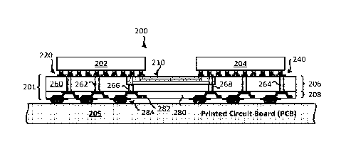
[0037] FIG. 2
illustrates an example of an integrated device package that includes
high density die-to-die interconnects. Specifically, FIG. 2 illustrates an
example of an
integrated device package 200 that includes a base 201, a first die 202, a
second die 204,
CA 02991933 2018-01-09
WO 2017/034641
PCT/US2016/035895
and a bridge 210. The bridge 210 may be configured to provide high density die-
to-die
interconnects. The integrated device package 200 may be coupled to a printed
circuit
board (PCB) 205.
[0038] The base 201
may be an integrated device package base. For example, the
base 201 may be a package substrate. The base 201 includes an encapsulation
portion
206 and a redistribution portion 208. The encapsulation portion 206 is coupled
to the
redistribution portion 208. The encapsulation portion 206 includes an
encapsulation
layer 260, the bridge 210, and at least one via (e.g., via 266) that is
coupled to the bridge
210. The bridge 210 is at least partially embedded in the encapsulation layer
260. The
bridge 210 is configured to provide a first electrical path for a first signal
(e.g., input
output signal) between the first die 202 and the second die 204. The at least
one via and
the bridge 210 are configured to provide a second electrical path for a second
signal
(e.g., power signal) to the first die 202.
[0039] As shown in
FIG. 2, the first die 202 is coupled to the base 201 through a
first set of interconnects 220. The first set of interconnects 220 may include
posts,
pillars and/or solder. The second die 204 is coupled to the base 201 through a
second set
of interconnects 240. The second set of interconnects 240 may include posts,
pillars
and/or solder.
High Density Interconnect Bridge Comprising Through Substrate Vias
[0040] FIG. 2
illustrates that the bridge 210 is located at least partially in the base
201. Specifically, the bridge 210 is at least partially embedded in the
encapsulation
portion 206. As shown in FIG. 2, the bridge 210 is at least partially embedded
in the
encapsulation layer 260. The bridge 210 may comprise a silicon bridge, a glass
bridge,
and/or a ceramic bridge. As mentioned above, the bridge 210 is configured to
provide
high density die-to-die interconnects in the integrated device package 200.
For example
the bridge 210 is configured to provide high density interconnects between the
first die
202 and the second die 204 (e.g., high density electrical paths for signals
(e.g.,
input/output signals) between the first die 202 and the second die 204). Thus,
in one
example, the bridge 210 may be configured to provide at least one first
electrical path
for at least one first signal between the first die 202 and the second die
204. The at least
one first electrical path for at least one first signal may include and/or may
be defined
by several interconnects (e.g., traces, vias) in the bridge 210. Such
interconnects that
CA 02991933 2018-01-09
WO 2017/034641
PCT/US2016/035895
8
define the at least one first electrical path are further described in detail
below in at least
FIGS. 4-5.
[0041] High density
interconnects and/or high density electrical paths may refer to
any density of wiring or connections per unit area than conventional printed
circuit
boards and may comprise finer lines and pitch, smaller vias and capture pads,
as well as
higher connection pad density. High density interconnects may thus be useful
to reduce
the size, thickness, weight, etc. of the package and/or device as well as
enhancing
electrical and thermal performance. High density interconnects may be defined
by
interconnects that include a width of about 2 microns (m) or less, a pitch of
about 4
microns (m) or less, and/or a spacing of about 2 microns (pm) or less. The
pitch of
interconnects may be a center to center distance between two adjacent
interconnects.
The spacing of interconnects may be an edge to edge distance between two
adjacent
interconnects. Examples of width, pitch and spacing for high density
interconnects are
further described below in at least FIGS. 4-5.
[0042] The bridge
210 may include a substrate, a dielectric layer, a set of high
density interconnects (e.g., traces, vias), and at least one through substrate
via (TSV).
The substrate may comprise silicon, glass and/or ceramic. The substrate, the
dielectric
layer, the set of high density interconnects (e.g., traces, vias), and the
through substrate
via (TSV) of the bridge 210 are not numbered or labeled in FIG. 2. However, a
detailed
exemplary bridge is illustrated and described below in at least FIGS. 4-5.
[0043] As shown in
FIG. 2, the first die 202 is coupled to (e.g., in communication
with) the second die 204 through at least the bridge 210. Specifically, FIG. 2
illustrates
that the first die 202 is coupled to the second die 204 through the first set
of
interconnects 220, interconnects (e.g., vias, traces) in the bridge 210, and
the second set
of interconnects 240. In some implementations, the first set of interconnects
220,
interconnects (e.g., vias, traces) in the bridge 210, and the second set of
interconnects
240 provide several high density electrical paths for signals (e.g.,
input/output signals)
between the first die 202 and the second die 204.
[0044] In some
implementations, at least one through substrate via (TSV) is
configured to provide at least one electrical path for a power signal and/or a
ground
reference signal to and/from a die coupled to the bridge 210. FIG. 2
illustrates that at
least one power signal and/or a ground reference signal can traverse through
the bridge
210 to the first die 202 and/or the second die 204. For example, the bridge
210 is
CA 02991933 2018-01-09
WO 2017/034641
PCT/US2016/035895
9
configured to provide a second electrical path for a second signal (e.g.,
power signal) to
the first die 202.
[0045] There are
several advantages to providing a bridge that includes at least one
TSV configured to provide an electrical path for a power signal and/or ground
reference
signal to and from one or more dies. First, an electrical path through the
bridge 210 is a
more direct path to and from a die, which means a shorter path to and from the
die.
Second, an electrical path through the bridge 210 means that the electrical
path does not
need to be routed around the bridge, saving space and real estate in the base
201, which
can result in an overall smaller form factor for the integrated device package
200. Third,
a more direct path for the power signal and/or ground reference signal means
that less
material is used, thereby reducing the cost of fabricating the integrated
device package.
[0046] Fourth, high
frequency die-to-die communication through a bridge may
require a die-to-die (D2D) buffer (which is not shown). In some
implementations, the
D2D buffer is located in a die coupled to a bridge (e.g., in the die portion
that is
vertically over the bridge) that is adapted and/or configured to provide die-
to-die
communication. Each die that is coupled to a bridge may include its own
respective
D2D buffer. The D2D buffer may include at least one transistor. The D2D buffer
may
need a power supply (e.g., power signal), and it may be important to have the
smallest
possible power voltage drop in the signal (e.g., in the power signal) to the
D2D buffer
(e.g., to a transistor of the D2D buffer). This can be achieved by routing the
power
signal to the D2D buffer (e.g., D2D of the die) through the bridge. A die may
have an
interconnect to the D2D buffer, that has a metal thickness (e.g., copper
thickness) of
about 2 microns (gm) or less and a lateral length that is greater than 1000
microns (p.m),
which produces a high IR drop in the power signal, where IR is a current
resistance. In
contrast, an interconnect through a bridge to the D2D buffer may have a length
of about
100 microns (pm) and a metal thickness (e.g., copper thickness) of about 10
microns
(pm), which provides less voltage drop to the D2D buffer, and thus provides
improved
die-to-die communication performance.
[0047] FIG. 2 shows
a high level illustration of a high density interconnect bridge
(e.g., bridge 210) that includes at least one TSV configured to provide at
least one
electrical path for a power signal and/or ground reference signal to and from
at least one
die. As mentioned above, a more detailed description of high density bridges
that
include at least one TSV configured to provide an electrical path for power
signals
CA 02991933 2018-01-09
WO 2017/034641
PCT/US2016/035895
to
and/or ground reference signals are further illustrated and described below in
at least
FIGS. 4-10.
Integrated Device Package Base Comprising High Density Interconnect Bridge
That Includes TSVs
[0048] As mentioned
above, the base 201 includes the encapsulation portion 206
and the redistribution portion 208. The base 201 may be an integrated device
package
base and/or a package substrate of the integrated device package 200.
[0049] The
encapsulation portion 206 includes an encapsulation layer 260, a first set
of vias 262, a second set of vias 264, a third set of vias 266, and a fourth
set of vias 268.
A set of vias may include one or more vias. The encapsulation layer 260 may
include
one of at least a mold and/or an epoxy fill. In some implementations, the
encapsulation
layer 260 may be a litho-pattemable layer (e.g., litho-etchable layer). The
litho-
pattemable layer is a material that is photo pattemable and developable (e.g.,
photo
etchable). That is, the encapsulation layer 260 is made of a material that can
be
patterned, developed, etched and/or removed through the exposure of the
material to a
light source (e.g., ultraviolet (UV) light). The bridge 210 is at least
partially embedded
in the encapsulation portion 206 and/or the encapsulation layer 260. Thus, the
encapsulation portion 206 and/or the encapsulation layer 260 at least
partially
encapsulates the bridge 210. The encapsulation layer 260 may be a mold and/or
an
epoxy fill. In some implementations, the encapsulation laver 260 is a layer
that includes
filler. In some implementations, the encapsulation layer 260 may have higher
concentration of filler material than a Polyimide (PI) layer and/or a
Polybenzoxazole
(PBO) layer.
[0050] The first
set of vias 262 vertically traverses at least part of the encapsulation
layer 260. Thus, the first set of vias 262 is located and/or embedded in the
encapsulation
layer 260. The first set of vias 262 is coupled to the redistribution portion
208. The first
set of vias 262 is also coupled to the first die 202 through the first set of
interconnects
220. In some implementations, the encapsulation portion 206 includes a set of
pads. The
set of pads may be coupled to the first set of vias 262 and the first set of
interconnects
220. Examples of pads in an encapsulation portion are further described below
in at
least FIGS. 6-10.
[0051] The second
set of vias 264 vertically traverses at least part of the
encapsulation layer 260. Thus, the second set of vias 264 is located and/or
embedded in
CA 02991933 2018-01-09
WO 2017/034641
PCT/US2016/035895
the encapsulation layer 260. The second set of vias 264 is coupled to the
redistribution
portion 208. The second set of vias 264 is also coupled to the second die 204
through
the second set of interconnects 240. In some implementations, the
encapsulation portion
206 includes a set of pads. The set of pads may be coupled to the second set
of vias 264
and the second set of interconnects 240.
[0052] The third
set of vias 266 vertically traverses at least part of the encapsulation
layer 260. Thus, the third set of vias 266 is located and/or embedded in the
encapsulation layer 260. The third set of vias 266 is coupled to the
redistribution portion
208. The third set of vias 266 is also coupled to the first die 202 through
the bridge 210
and the first set of interconnects 220. The third set of vias 266 is coupled
to the through
substrate vias (TSVs) of the bridge 210. In some implementations, the
encapsulation
portion 206 includes a set of pads. The set of pads may be coupled to the
bridge 210 and
the first set of interconnects 220.
[0053] In some
implementations, the third set of vias 266 is configured to provide at
least one electrical path for at least one power signal and/or at least one
ground
reference signal to and from a die (e.g., first die 202), through the bridge
210. For
example, in some implementations, a via (e.g., from the vias 266) and the
bridge 210
may be configured to provide a second electrical path for a second signal
(e.g., power
signal) to the first die 202.
[0054] The fourth
set of vias 268 vertically traverses at least part of the
encapsulation layer 260. The fourth set of vias 268 is coupled to the
redistribution
portion 208. The fourth set of vias 268 is also coupled to the second die 204
through the
bridge 210 and the second set of interconnects 240. The fourth set of vias 268
is coupled
to the through substrate vias (TSVs) of the bridge 210. In some
implementations, the
encapsulation portion 206 includes a set of pads. The set of pads may be
coupled to the
bridge 210 and the second set of interconnects 240,
[0055] In some
implementations, the fourth set of vias 268 is configured to provide
at least one electrical path for at least one power signal and/or at least one
ground
reference signal to and from a die (e.g., second die 204), through the bridge
210.
[0056] In some
implementations, the vias in the encapsulation portion 206 are vias
that have a width / diameter of about 10 microns (j.un) or less, and/or a
spacing of about
microns (rim) or less. Thus, in some implementations, the vias in the
encapsulation
portion 206 are interconnects that have lower density than the interconnects
in the
bridge 210. In some implementations, at least a majority of the vias in the
encapsulation
CA 02991933 2018-01-09
WO 2017/034641
PCT/US2016/035895
12
portion 206 have lower density (e.g., greater width, greater spacing) than the
interconnects (e.g., traces, vias) in the bridge 210.
100571 The vias
(e.g., first set of vias 262, second set of vias 264, third set of vias
266, fourth set of vias 268) may have different shapes and sizes. Various
examples of
shapes for the vias in the encapsulation layer are further illustrated and
described below
in at least FIGS. 6-10,
100581 The
redistribution portion 208 includes a set of dielectric layers 280, and a
set of interconnects 282. The set of dielectric layers 280 may include one or
more
dielectric layers. As shown in FIG. 2, the redistribution portion 208 is
coupled to a first
surface (e.g., bottom surface) of the encapsulation portion 206. The set of
interconnects
282 may include a trace, a via, a pad, a redistribution interconnect, and/or
an under
bump metallization (UBM) layer. As further shown in FIG. 2, the set of
interconnects
282 includes redistribution interconnects and UBM layers. The set of
interconnects 282
is coupled to the first set of vias 262, the second set of vias 264, the third
set of vias
266, and the fourth set of vias 268. Some of the set of interconnects 282 may
be
configured to provide at least one electrical path for at least one power
signal and/or at
least one ground reference signal. In some implementations, the set of
interconnects 282
in the redistribution portion 208 are interconnects that have a width of about
5 microns
(lam) or less, and/or a spacing of about 5 microns (l_tm) or less. More
detailed examples
of various redistribution portions are further described in at least FIGS. 6-
10. FIG. 2
illustrates a set of solder balls 284 that is coupled to the set of
interconnects 282. In
some implementations, the set of solder balls 284 is coupled to UBM layers of
the set of
interconnects 282. The set of solder balls 284 is coupled to the PCB 205.
[0059] Although not
shown, the integrated device package 200 may also include
another encapsulation layer that covers the first die 202 and the second die
204. The
encapsulation layer may include one of at least a mold and/or an epoxy fill.
Exemplary Integrated Device Package Comprising Bridge in Litho-Etchable Layer
[0060] FIG. 3
illustrates another example of an integrated device package that
includes high density die-to-die interconnects. Specifically, FIG. 3
illustrates an
example of an integrated device package 300 that includes a base 301, the
first die 202,
the second die 204, and the bridge 210. The base 301 may be an integrated
device
package base and/or a package substrate of the integrated device package 300.
The base
CA 02991933 2018-01-09
WO 2017/034641
PCT/US2016/035895
13
301 includes the encapsulation portion 206 and a redistribution portion 308.
The
integrated device package 300 is coupled to the printed circuit board (PCB)
205.
100611 The
integrated device package 300 is similar to the integrated device
package 200, except that in some implementations, the redistribution portion
308
includes a different configuration of interconnects.
[0062] As shown in
FIG. 3, the first die 202 is coupled to the base 201 through the
first set of interconnects 220. The first set of interconnects 220 may include
posts,
pillars and/or solder. The second die 204 is coupled to the base 201 through
the second
set of interconnects 240. The second set of interconnects 240 may include
posts, pillars
and/or solder.
[0063] As shown in
FIG. 3, the redistribution portion 308 is coupled to the
encapsulation portion 206. The redistribution portion 308 includes a set of
dielectric
layers 280, and a set of interconnects 382. The set of dielectric layers 280
may include
one or more dielectric layers. As shown in FIG. 3, the redistribution portion
308 is
coupled to a first surface (e.g., bottom surface) of the encapsulation portion
206. The set
of interconnects 382 may include a trace, a via, a pad, a redistribution
interconnect,
and/or an under bump metallization (UBM) layer. As further shown in FIG. 3,
the set of
interconnects 382 includes pads, vias, traces, and UBM layers. The set of
interconnects
382 is coupled to the first set of vias 262, the second set of vias 264, the
third set of vias
266, and the fourth set of vias 268. Some of the set of interconnects 382 may
be
configured to provide at least one electrical path for at least one power
signal and/or at
least one ground reference signal. In some implementations, the set of
interconnects 382
in the redistribution portion 308 are interconnects that have a width of about
5 microns
(pm) or less, and/or a spacing of about 5 microns (pm) or less. More detailed
examples
of various redistribution portions are further described in at least FIGS. 6-
10. FIG. 3
illustrates the set of solder balls 284 is coupled to the set of interconnects
382. In some
implementations, the set of solder balls 284 is coupled to UBM layers of the
set of
interconnects 382. The set of solder balls 284 is coupled to the PCB 205.
[0064] Although not
shown, the integrated device package 300 may also include
another encapsulation laver that covers the first die 202 and the second die
204. The
encapsulation layer may include one of at least a mold and/or an epoxy fill.
Exemplary Bridge Comprising Interconnects and Through Substrate Vias (TSVs)
CA 02991933 2018-01-09
WO 2017/034641
PCT/US2016/035895
14
[0065] As mentioned
above, an integrated device package may include a bridge
(e.g., silicon bridge, glass bridge, ceramic bridge) that is configured to
provide high
density die-to-die interconnects, and through substrate vias (TSVs) configured
to
provide at least one electrical path for at least one power signal and/or at
least one
ground reference signal to and from one or more dies. FIGS. 4 and 5 illustrate
conceptual examples of such bridges configured to provide high density
interconnects
and TSVs in an integrated device package.
[0066] FIG. 4
illustrates a profile view of an example of the bridge 210 (e.g., silicon
bridge). The bridge 210 includes a substrate 402, a dielectric layer 404, at
least one first
interconnect 406, at least one second interconnect 408, at least one third
interconnect
410, at least one fourth interconnect 418, and at least one fifth interconnect
420. In some
implementations, the bridge 210 may be implemented in any of the integrated
device
package illustrated and described in the present disclosure. For example, the
bridge 210
may be the bridge of FIGS. 2-3. In some implementations, the bridge 210 is a
means
(e.g., bridge means) for providing a die-to-die electrical path or die-to-die
electrical
connection between a first die and a second die. For example, the at least one
first
interconnect 406, the at least one second interconnect 408, and the at least
on third
interconnect 410 may define at least one first electrical path for at least
one first signal
between a first die and a second die. In some implementations, the at least
one first
interconnect 406, the at least one second interconnect 408, and the at least
on third
interconnect 410 may form at least one first set of interconnects that is
configured to
provide at least one first electrical path for at least one first signal
between a first die
and a second die.
[0067] In some
implementations, the bridge 210 is a means (e.g., bridge means) for
providing at least one second electrical path for at least a power signal
and/or at least a
ground reference signal to and from a first die. In some implementations, the
bridge 210
is a means (e.g., bridge means) for providing at least one third electrical
path for a least
a power signal and/or at least a ground reference signal to and from a second
die.
[0068] In some
implementations, the means (e.g., bridge means) provides an
interconnection density that is equal or higher than the interconnection
density of the
encapsulation portion (e.g., encapsulation portion 206) and/or the
redistribution portion
(e.g., redistribution portion 208) of an integrated device package base.
[0069] In some
implementations, the substrate 402 comprises a silicon substrate, a
glass substrate, and/or a ceramic substrate. The first interconnect 406 may be
at least
CA 02991933 2018-01-09
WO 2017/034641
PCT/US2016/035895
one trace located on the substrate 402. The dielectric layer 404 covers the
first
interconnect 406 and the substrate 402. In some implementations, the second
and third
interconnects 408 and 410 are vias that vertically traverses the dielectric
layer 404. The
second and third interconnects 408 and 410 are coupled to the first
interconnect 406.
[0070] In some
implementations, the first, second, and third interconnects 406, 408
and 410 are high density interconnects. In some implementations, high density
interconnects are interconnects that have a width of about 2 microns (gm) or
less, and/or
a spacing of about 2 microns (gm) or less. In some implementations, the width
of an
interconnect may be the width of the trace and/or line. In some
implementations, the
width of an interconnect may be the diameter of a via and/or a pad. A spacing
is an edge
to edge distance between two neighboring / adjacent interconnects.
[0071] The fourth
interconnect 418 may be a via that traverses the substrate 402 and
the dielectric layer 404. The fourth interconnect 418 may be a through
substrate via
(TSV) that traverses the substrate 402 and the dielectric layer 404. In some
implementations, the fourth interconnect 418 may be a combination of two or
more vias
(e.g., first via in the substrate 402 and a second via in the dielectric layer
404). In some
implementations, the fourth interconnect 418 is configured to provide at least
one
electrical path (e.g., second electrical path) for at least one second signal
(e.g., at least
one power signal and/or at least one ground reference signal) to and from a
die (e.g.,
first die).
[0072] The fifth
interconnect 420 may be a via that traverses the substrate 402 and
the dielectric layer 404. The fifth interconnect 420 may be a through
substrate via (TSV)
that traverses the substrate 402 and the dielectric layer 404. In some
implementations,
the fifth interconnect 420 may be a combination of two or more vias (e.g.,
first via in the
substrate 402 and a second via in the dielectric layer 404). In some
implementations, the
fifth interconnect 420 is configured to provide at least one electrical path
(e.g., third
electrical path) for at least one third signal (e.g., at least one power
signal and/or at least
one ground reference signal) to and from a die (e.g., second die). In some
implementations, the fourth and fifth interconnects 418 and 420 are high
density
interconnects.
[0073] It is noted
that the bridge 210 may include several first interconnects, second
interconnects, third interconnects, fourth interconnects, and fifth
interconnects.
[0074] FIG. 5
illustrates a plan view (e.g., top view) of an example of the bridge
210 (e.g., silicon bridge) that includes a substrate (not visible), the
dielectric layer 404,
CA 02991933 2018-01-09
WO 2017/034641
PCT/US2016/035895
16
the first interconnect 406, the second interconnect 408, the third
interconnect 410, the
fourth interconnect 418, and the fifth interconnect 420. FIG. 5 illustrates
the width and
spacing of interconnects. The width of an interconnect is illustrated by (W),
and the
spacing between two neighboring / adjacent interconnects is illustrated by
(S). In some
implementations, the first interconnect 406, the second interconnect 408, the
third
interconnect 410, the fourth interconnect 418, and/or the fifth interconnect
420 are high
density interconnects. In some implementations, high density interconnects are
interconnects that have a width of about 2 microns (um) or less, and/or a
spacing of
about 2 microns (p.m) or less.
[0075] As described
above, there are several advantages in providing a bridge that
includes at least one TSV configured to provide an electrical path for a power
signal
and/or ground reference signal to and from one or more dies. First, an
electrical path
through the bridge 210 is a more direct path to and from a die, which means a
shorter
path to and from the die. Second, an electrical path through the bridge 210
means that
the electrical path does not need to be routed around the bridge, saving space
and real
estate in the base 201, which can result in an overall smaller form factor for
the
integrated device package 200. Third, a more direct path for the power signal
and/or
ground reference signal means that less material is used, thereby reducing the
cost of
fabricating the integrated device package. Fourth, TSVs may help provide
improved
performance in die-to-die communication.
Exemplary Integrated Device Package Comprising Bridge Litho-Etchable Layer
[0076] Having
described an example of an integrated device package that includes
high density die-to-die interconnects in general detail, examples of
integrated device
packages that includes high density die-to-die interconnects and through
substrate vias
(TSVs) will now be described in more detail.
[0077] FIG. 6
illustrates an example of a portion of integrated device package base
600 of an integrated device package. In some implementations, the integrated
device
package base 600 may correspond to at least the encapsulation portion 206 and
the
redistribution portion 208 of FIG. 2. In some implementations, the integrated
device
package base 600 is a package substrate of an integrated device package.
[0078] The
integrated device package base 600 includes an encapsulation portion
602 and a redistribution portion 604. The encapsulation portion 602 includes
an
encapsulation layer 606, a first via 603, a second via 605, a first pad 611, a
second pad
CA 02991933 2018-01-09
WO 2017/034641
PCT/US2016/035895
17
613, a third pad 615, a solder resist layer 608, and the bridge 210. In some
implementations, the encapsulation layer 606 is a litho-patternable material
(e.g., litho-
etchable material) that is photo pattemable and developable (e.g., photo
etchable). That
is, the encapsulation layer 606 is made of a material that can be patterned,
develop,
etched and/or removed through the exposure of the material to a light source
(e.g.,
ultraviolet (UV) light). The encapsulation layer 606 may include one of at
least a mold
and/or an epoxy fill.
[0079] The first
via 603 vertically traverses the encapsulation layer 606. The first
pad 611 is coupled to the first via 601 The second via 605 vertically
traverses the
encapsulation layer 606. Thus, the second via 605 is located and/or embedded
in the
encapsulation layer 606. The second via 605 is coupled to the interconnect 418
of the
bridge 210. The interconnect 418 may be a through substrate via (TSVs) of the
bridge
210. The second pad 613 is coupled to the interconnect 418. In some
implementations,
the second via 605, the interconnect 418, and the second pad 613 are
configured to
provide an electrical path (e.g., second electrical path) for a second signal
(e.g., a power
signal and/or a ground reference signal) to and from a die (e.g., first die
202).
[0080] The solder
resist layer 608 covers a first surface (e.g., top surface) of the
encapsulation layer 606. A solder ball may be coupled to the pads 611, 613,
and/or 615.
The via 603 is part of a set of vias in the encapsulation layer 606, where the
set of vias
has a first density (e.g., first width and/or first spacing).
[0081] FIG. 6 also
illustrates that the bridge 210 is at least partially embedded in the
encapsulation layer 606 of the encapsulation portion 602. The bridge 210 is
configured
to provide high density electrical paths (e.g., high density die-to-die
interconnects) in
the encapsulation portion 602. The bridge 210 is also configured to provide an
electrical
path for a signal (e.g., power signal) to a die through the substrate 402 of
the bridge 210.
[0082] The
redistribution portion 604 is coupled to the encapsulation portion 602.
The redistribution portion 604 includes a first dielectric layer 642, a second
dielectric
layer 644, and a third dielectric layer 648, an interconnect 643, and an
interconnect 653.
In some implementations, the first, second, and/or third dielectric layers
642, 644,
and/or 648 may be collectively a single dielectric layer. The interconnects
643 and 653
may be redistribution interconnects comprising a diagonal portion and a
horizontal
portion. In some implementations, the interconnects 643 and 653 are U or V
shaped
redistribution interconnects. In some implementations, the interconnects 643
and 653
may be configured to couple to solder balls (e.g., printed circuit board side
solder balls).
CA 02991933 2018-01-09
WO 2017/034641
PCT/US2016/035895
18
[0083] The
interconnect 643 of the redistribution portion 604 is coupled to the via
603 of the encapsulation portion 602. The interconnect 653 of the
redistribution portion
604 is coupled to the second via 605 in the encapsulation portion 602. In some
implementations, the interconnect 653, the second via 605, the interconnect
418, and the
second pad 613 are configured to provide an electrical path for a power signal
and/or a
ground reference signal to and from a die (e.g., first die 202).
[0084] In some
implementations, a first die (e.g., die 202) may be electrically
coupled to a second die (e.g., second die 204) through the third pad 615, the
interconnect 410, and the interconnect 406. In some implementations, the third
pad 615,
the interconnect 410, and the interconnect 406 define an electrical path for
die-to-die
connection between the first and second dies (e.g., dies 202 and 204).
Exemplary Integrated Device Package Comprising Bridge Litho-Etchable Layer
[0085] FIG. 7
illustrates another example of a portion of integrated device package
base 700 of an integrated device package. In some implementations, the
integrated
device package base 700 may correspond to at least the encapsulation portion
206 and
the redistribution portion 308 of FIG. 3. In some implementations, the
integrated device
package base 700 is a package substrate of an integrated device package.
[0086] The
integrated device package base 700 includes an encapsulation portion
602 and a redistribution portion 704. The encapsulation portion 602 includes
an
encapsulation layer 606, a first via 603, a second via 605, a first pad 611, a
second pad
613, a third pad 615, a solder resist layer 608, and the bridge 210. In some
implementations, the encapsulation layer 606 is a litho-pattemable material
(e.g., litho-
etchable material) that is photo pattemable and developable (e.g., photo
etchable). That
is, the encapsulation layer 606 is made of a material that can be patterned,
develop,
etched and/or removed through the exposure of the material to a light source
(e.g.,
ultraviolet (UV) light). The encapsulation layer 606 may include one of at
least a mold
and/or an epoxy fill.
[0087] The first
via 603 vertically traverses the encapsulation layer 606. The first
pad 611 is coupled to the first via 603. The second via 605 vertically
traverses the
encapsulation layer 606. The second via 605 is coupled to the interconnect 418
of the
bridge 210. The interconnect 418 may be a through substrate via (TSVs) of the
bridge
210. The second pad 613 is coupled to the interconnect 418. In some
implementations,
the second via 605, the interconnect 418, and the second pad 613 are
configured to
CA 02991933 2018-01-09
WO 2017/034641
PCT/US2016/035895
19
provide an electrical path for a power signal and/or a ground reference signal
to and
from a die (e.g., first die 202).
[0088] The solder
resist layer 608 covers a first surface (e.g., top surface) of the
encapsulation layer 606. A solder ball may be coupled to the pads 611, 613,
and/or 615.
The via 603 is part of a set of vias in the encapsulation layer 606, where the
set of vias
has a first density (e.g., first width and/or first spacing).
[0089] FIG. 7 also
illustrates that the bridge 210 is at least partially embedded in the
encapsulation layer 606 of the encapsulation portion 602. The bridge 210 is
configured
to provide high density electrical paths (e.g., high density die-to-die
interconnects) in
the encapsulation portion 602. The bridge 210 is also configured to provide an
electrical
path for a signal (e.g., power signal) to a die through the substrate 402 of
the bridge 210.
[0090] The
redistribution portion 704 is coupled to the encapsulation portion 602.
The redistribution portion 704 includes a first dielectric layer 642, a second
dielectric
layer 644, and a third dielectric layer 648, an interconnect 743, an
interconnect 745, an
interconnect 753, and an interconnect 755. In some implementations, the first,
second,
and/or third dielectric layers 642, 644, and/or 648 may be collectively a
single dielectric
layer. The interconnects 743 and 753 may be vias. The interconnects 745 and
755 may
be traces and/or pads. In some implementations, the interconnects 745 and 755
may be
configured to couple to solder balls (e.g., printed circuit board side solder
balls).
[0091] The
interconnect 745 is coupled to the interconnect 743. The interconnect
743 of the redistribution portion 704 is coupled to the via 603 of the
encapsulation
portion 602. The interconnect 755 is coupled to the interconnect 753. The
interconnect
753 of the redistribution portion 704 is coupled to the second via 605 in the
encapsulation portion 602. In some implementations, the interconnect 755, the
interconnect 753, the second via 605, the interconnect 418, and the second pad
613 are
configured to provide an electrical path for a power signal and/or a ground
reference
signal to and from a die (e.g., first die 202).
[0092] In some
implementations, a first die (e.g., die 202) may be electrically
coupled to a second die (e.g., second die 204) through the third pad 615, the
interconnect 410, and the interconnect 406. In some implementations, the third
pad 615,
the interconnect 410, and the interconnect 406 define an electrical path for
die-to-die
connection between the first and second dies (e.g., dies 202 and 204).
Exemplary Integrated Device Package Comprising Bridge Litho-Etchable Layer
CA 02991933 2018-01-09
WO 2017/034641
PCT/US2016/035895
[0093] FIGS. 6-7
illustrate vias (e.g., via 603, via 605) in an encapsulation layer
comprising a certain shapes. As shown in FIGS. 6-7 the vias in the
encapsulation layer
606 are formed by filling cavities in the encapsulation layer 606. However, in
some
implementations, the vias in an encapsulation layer may have a different shape
and/or
configuration.
[0094] FIGS. 8-9
illustrate vias in an encapsulation layer comprising different
shapes. As shown in FIGS. 8-9 and further described below, the vias in the
encapsulation layer are formed by conform fill, where one or more metal layers
are
formed on the walls of the cavities leaving another cavity that is filled with
a dielectric
layer. In some implementations, the vias have a bowl or can-like shape.
[0095] FIG. 8
illustrates an example of a portion of integrated device package base
800 of an integrated device package. In some implementations, the integrated
device
package base 800 may correspond to at least the encapsulation portion 206 and
the
redistribution portion 208 of FIG. 2. In some implementations, the integrated
device
package base 800 is a package substrate of an integrated device package.
[0096] The
integrated device package base 800 includes an encapsulation portion
802 and a redistribution portion 804. The encapsulation portion 802 includes
an
encapsulation layer 606, a first via 803, a second via 805, a first pad 611, a
second pad
613, a third pad 615, a solder resist layer 608, and the bridge 210. In some
implementations, the encapsulation layer 606 is a litho-pattemable material
(e.g., litho-
etchable material) that is photo pattemable and developable (e.g., photo
etchable). That
is, the encapsulation layer 606 is made of a material that can be patterned,
develop,
etched and/or removed through the exposure of the material to a light source
(e.g.,
ultraviolet (UV) light). The encapsulation layer 606 may include one of at
least a mold
and/or an epoxy fill.
[0097] As shown in
FIG. 8, the first via 803 includes a V shape profile cross section
or a U shape profile cross section. The first via 803 may be a conform fill
via that forms
the shape of the cavity in which it is formed. In this example, the first via
803 is formed
along at least the walls of the cavity in which it is formed. The first via
803 also
includes a wing portion that is formed in the redistribution portion 804. The
wing
portion of the first via 803 traverses laterally in the redistribution portion
804. The wing
portion may be referred to as a wing interconnect of the via. The first via
803 vertically
traverses the encapsulation layer 606. The first pad 611 is coupled to the
first via 803.
The second via 805 also includes a V shape profile cross section or a U shape
profile
CA 02991933 2018-01-09
WO 2017/034641
PCT/US2016/035895
2
cross section. The second via 805 may be a conform fill via that forms the
shape of the
cavity in which it is formed. In this example, the second via 805 is formed
along at least
the walls of the cavity in which it is formed. The second via 805 also
includes a wing
portion that is formed in the redistribution portion 804. The wing portion of
the second
via 805 traverses laterally in the redistribution portion 804. A dielectric
layer 840 is
located within the cavity created by the vias (e.g., via 803, via 805) of the
encapsulation
layer 606. The second via 805 vertically traverses the encapsulation layer
606. Thus, the
second via 805 is at least partially located and/or at least partially
embedded in the
encapsulation layer 606. The second via 805 is coupled to the interconnect 418
of the
bridge 210. The interconnect 418 may be a through substrate via (TSVs) of the
bridge
210. The second pad 613 is coupled to the interconnect 418. In some
implementations,
the second via 805, the interconnect 418, and the second pad 613 are
configured to
provide an electrical path for a power signal and/or a ground reference signal
to and
from a die (e.g., first die 202).
[0098] The solder
resist layer 608 covers a first surface (e.g., top surface) of the
encapsulation layer 606. A solder ball may be coupled to the pads 611, 613,
and/or 615,
The via 803 is part of a set of vias in the encapsulation layer 606, where the
set of vias
has a first density (e.g., first width and/or first spacing).
[0099] FIG. 8 also
illustrates that the bridge 210 is at least partially embedded in the
encapsulation layer 606 of the encapsulation portion 802. The bridge 210 is
configured
to provide high density electrical paths (e.g., high density die-to-die
interconnects) in
the encapsulation portion 802. The bridge is also configured to provide an
electrical
path for a signal (e.g., power signal) to a die through the substrate 402 of
the bridge 210.
[00100] The redistribution portion 804 is coupled to the encapsulation portion
802.
The redistribution portion 804 includes dielectric layer 840, a dielectric
layer 844, and a
dielectric layer 848, an interconnect 843, and an interconnect 853, In some
implementations, the dielectric layers 840, 844, and/or 848 may be
collectively a single
dielectric layer. The interconnects 843 and 853 may be redistribution
interconnects
comprising a diagonal portion and a horizontal portion. In some
implementations, the
interconnects 843 and 853 include U or V shaped redistribution interconnects.
In some
implementations, the interconnects 843 and 853 may be configured to couple to
solder
balls (e.g., printed circuit board side solder balls).
[00101] The interconnect 843 of the redistribution portion 804 is coupled to
the via
803 of the encapsulation portion 802 (e.g., coupled to wing portion of the
first via 803).
CA 02991933 2018-01-09
WO 2017/034641
PCT/US2016/035895
22
The interconnect 853 of the redistribution portion 804 is coupled to the
second via 805
(e.g., coupled to wing portion of the second via 805) in the encapsulation
portion 802.
In some implementations, the interconnect 853, the second via 805, the
interconnect
418, and the second pad 613 are configured to provide an electrical path for a
power
signal and/or a ground reference signal to and from a die (e.g., first die
202).
[00102] FIG. 8
illustrates that the redistribution portion 804 may also include a first
under bump metallization (UBM) layer 845 and a second under bump metallization
(UBM) layer 855. The first UBM layer 845 is coupled to the interconnect 843.
The
second UBM layer 855 is coupled to the interconnect 853. In some
implementations, the
first UBM layer 845 and the second UBM layer 855 are configured to couple to
solder
balls.
[00103] In some
implementations, a first die (e.g., die 202) may be electrically
coupled to a second die (e.g., second die 204) through the third pad 615, the
interconnect 410, and the interconnect 406. In some implementations, the third
pad 615,
the interconnect 410, and the interconnect 406 define an elechical path for
die-to-die
connection between the first and second dies (e.g., dies 202 and 204).
Exemplary Integrated Device Package Comprising Bridge Litho-Etchable Layer
[00104] FIG. 9
illustrates another example of a portion of integrated device package
base 900 of an integrated device package. In some implementations, the
integrated
device package base 900 may correspond to at least the encapsulation portion
206 and
the redistribution portion 308 of FIG. 3. In some implementations, the
integrated device
package base 900 is a package substrate of an integrated device package.
[00105] The integrated device package base 900 includes an encapsulation
portion
802 and a redistribution portion 904. The encapsulation portion 802 includes
an
encapsulation layer 606, a first via 803, a second via 805, a first pad 611, a
second pad
613, a third pad 615, a solder resist layer 608, and the bridge 210. In some
implementations, the encapsulation layer 606 is a litho-pahernable material
(e.g., litho-
etchable material) that is photo pattemable and developable (e.g., photo
etchable). That
is, the encapsulation layer 606 is made of a material that can be patterned,
develop,
etched and/or removed through the exposure of the material to a light source
(e.g.,
ultraviolet (UV) light). The encapsulation layer 606 may include one of at
least a mold
and/or an epoxy fill.
CA 02991933 2018-01-09
WO 2017/034641
PCT/US2016/035895
23
[00106] As shown in
FIG. 9, the first via 803 includes a V shape profile cross section
or a U shape profile cross section. The first via 803 may be a conform fill
via that forms
the shape of the cavity in which it is formed, In this example, the first via
803 is formed
along at least the walls of the cavity in which it is formed. The first via
803 also
includes a wing portion that is formed in the redistribution portion 904. The
wing
portion of the first via 803 traverses laterally in the redistribution portion
904. The wing
portion may be referred to as a wing interconnect of the via. The first via
803 vertically
traverses the encapsulation layer 606. The first pad 611 is coupled to the
first via 803.
The second via 805 also includes a V shape profile cross section or a U shape
profile
cross section. The second via 805 may be a conform fill via that forms the
shape of the
cavity in which it is formed. In this example, the second via 805 is formed
along at least
the walls of the cavity in which it is formed. The second via 805 also
includes a wing
portion that is formed in the redistribution portion 904. The wing portion of
the second
via 805 traverses laterally in the redistribution portion 904. A dielectric
layer 840 is
located within the cavity created by the vias (e.g., via 803, via 805) of the
encapsulation
layer 606. The second via 805 vertically traverses the encapsulation layer
606. The
second via 805 is coupled to the interconnect 418 of the bridge 210. The
interconnect
418 may be a through substrate via (TSVs) of the bridge 210. The second pad
613 is
coupled to the interconnect 418. In some implementations, the second via 805,
the
interconnect 418, and the second pad 613 are configured to provide an
electrical path for
a power signal and/or a ground reference signal to and from a die (e.g., first
die 202).
1001071 The solder
resist layer 608 covers a first surface (e.g., top surface) of the
encapsulation layer 606. A solder ball may be coupled to the pads 611, 613,
and/or 615.
The via 803 is part of a set of vias in the encapsulation layer 606, where the
set of vias
has a first density (e.g., first width and/or first spacing).
[00108] FIG. 9 also
illustrates that the bridge 210 is at least partially embedded in the
encapsulation layer 606 of the encapsulation portion 802. The bridge 210 is
configured
to provide high density electrical paths (e.g., high density die-to-die
interconnects) in
the encapsulation portion 802. The bridge is also configured to provide an
electrical
path for a signal (e.g,, power signal) to a die through the substrate 402 of
the bridge 210.
[00109] The redistribution portion 904 is coupled to the encapsulation portion
802.
The redistribution portion 904 includes a dielectric layer 840, a dielectric
layer 844, and
a dielectric layer 848, an interconnect 943, an interconnect 945, an
interconnect 953,
and an interconnect 955. In some implementations, the dielectric layers 842,
844, and/or
CA 02991933 2018-01-09
WO 2017/034641
PCT/US2016/035895
24
848 may be collectively a single dielectric layer. The interconnects 943 and
953 may be
vias. The interconnects 945 and 955 may be traces and/or pads. In some
implementations, the interconnects 945 and 955 may be configured to couple to
solder
balls (e.g., printed circuit board side solder balls).
1001101 The interconnect 945 is coupled to the interconnect 943. The
interconnect
943 of the redistribution portion 904 is coupled to the via 803 of the
encapsulation
portion 802 (e.g., coupled to the wing portion of the first via 803). The
interconnect 955
is coupled to the interconnect 953. The interconnect 953 of the redistribution
portion
904 is coupled to the second via 805 in the encapsulation portion 802 (e.g.,
coupled to
the wing portion of the second via 805). In some implementations, the
interconnect 955,
the interconnect 953, the second via 805, the interconnect 418, and the second
pad 613
are configured to provide an electrical path for a power signal and/or a
ground reference
signal to and from a die (e.g., first die 202).
1001111 FIG. 9
illustrates that the redistribution portion 904 may also include a first
under bump metallization (UBM) layer 947 and a second under bump metallization
(UBM) layer 957. The first UBM layer 947 is coupled to the interconnect 945.
The
second UBM layer 957 is coupled to the interconnect 955. In some
implementations, the
first UBM layer 947 and the second UBM layer 957 are configured to couple to
solder
balls.
[00112] In some
implementations, a first die (e.g., die 202) may be electrically
coupled to a second die (e.g., second die 204) through the third pad 615, the
interconnect 410, and the interconnect 406. In some implementations, the third
pad 615,
the interconnect 410, and the interconnect 406 define an electrical path for
die-to-die
connection between the first and second dies (e.g., dies 202 and 204).
Exemplary Integrated Device Package Comprising Bridge Litho-Etchable Layer
[00113] FIG. 10 illustrates an example of an integrated device package 1000
that
includes two dies coupled to an integrated device package base. As shown in
FIG. 10,
the integrated device package 1000 includes a first die 1002 and a second die
1004, and
the base 600. The first die 1002 and the second die 1004 are coupled to the
base 600. It
should be noted that the first die 1002 and the second die 1004 may be coupled
to any of
the integrated device package bases (e.g., base 201, base 301, base 700, base
800, base
900) described in the present disclosure.
CA 02991933 2018-01-09
WO 2017/034641
PCT/US2016/035895
[00114] The first die 1002 includes an under bump metallization (UBM) layer
1020
(optional), a pillar 1022, and solder 1024. The first die 1002 is coupled to
the integrated
device package base 600 through the UBM layer 1020 (optional), the pillar
1022, the
solder 1024, and the pad 613 of the integrated device package base 600.
[00115] The second die 1004 includes an under bump metallization (UBM) layer
1040 (optional), a pillar 1042, and solder 1044. The second die 1004 is
coupled to the
integrated device package base 600 through the UBM layer 1040 (optional), the
pillar
1042, the solder 1044, and the pad 623 of the integrated device package base
600.
[00116] As further
shown, a fill 1050 is located between the first die 1002 and the
integrated device package base 600. The fill 1050 may include at least a non-
conducting
fill (NCF) and/or a non-conducting paste (NCP). The fill 1050 covers the
interconnects
(e.g., pillar 1022, solder 1024, pad 613) between the first die 1002 and the
integrated
device package base 600. The fill 1050 is also located between the second die
1004 and
the integrated device package base 600.
Exemplary Sequence for Providing / Fabricating a High Density Interconnect
Bridge That Includes Through Substrate Vias (TSVs)
[00117] In some implementations, providing / fabricating a high density
interconnect
bridge with through substrate vias, includes several processes. FIG. 11
illustrates an
exemplary sequence for providing / fabricating a high density interconnect
bridge that
includes TSVs. In some implementations, the sequence of FIG. 11 may be used to
provide / fabricate the bridge of FIGS. 2-10 and/or other bridges described in
the
present disclosure. However, for the purpose of simplification, FIG. 11 will
be
described in the context of providing / fabricating the bridge of FIG. 4.
[00118] It should be noted that the sequence of FIG. 11 may combine one or
more
stages in order to simplify and/or clarify the sequence for providing /
fabricating a
bridge. In some implementations, the order of the processes may be changed or
modified.
[00119] Stage 1 of
FIG. 11, illustrates a state after a substrate 1102 is provided. In
some implementations, the substrate 1102 is provided by a supplier. In some
implementations, the substrate 1102 is fabricated (e.g., formed). In some
implementations, the substrate 1102 comprises a silicon substrate, a glass
substrate, a
ceramic substrate, and/or wafer (e.g., silicon wafer).
CA 02991933 2018-01-09
WO 2017/034641
PCT/US2016/035895
26
[00120] Stage 2
illustrates a state after cavities 1103 (e.g., cavity 1103a, cavity
1103b) are formed in the substrate 1102. Different implementations may form
the
cavities 1103 differently, In some implementations, a laser and/or a
lithography process
is used to form the cavities 1103.
[00121] Stage 3
illustrates a state after vias 1104 (e.g., via 1104a, via 1104b) are
formed in the cavities of the substrate 1102. The vias 1104 may be through
substrate
vias (TSVs). Different implementations may form the vias 1104 differently. For
example, a plating process and/or a pasting process may be use to form the
vias 1104.
[00122] Stage 4
illustrates a state after a metal layer 1106 is formed on the substrate
1102. In some implementations, the metal layer 1106 may form and/or define one
or
more high density interconnects (e.g., as described in FIGS. 4-5). These high
density
interconnects may be high density electrical paths between dies. In some
implementations, providing the metal layer 1106 includes forming (e.g.,
plating) one or
more metal layers (e.g., seed layer and metal layer) and selectively etching
portions of
the one or more metal layers. FIGS. 15-18 illustrate examples of forming one
or more
metal layers using several plating processes.
[00123] Stage 5
illustrates a state after a dielectric layer 1108 is formed over the
substrate 1102 and the metal layer 1106. Different implementations may use
different
materials for the dielectric layer 1108.
[00124] Stage 6
illustrates a state after the cavities 1109 (e.g., cavity 1109a, cavity
1109b) and the cavities 1111 (e.g., cavity 1111a, cavity 1111b) are formed in
the
dielectric layer 1108. Different implementations may use different processes
for
forming cavities in the dielectric layer 1108. In some implementations, a
laser may be
used to form the cavities. In some implementations, a photo etching process is
used to
form the cavities.
[00125] Stage 7
illustrates a state after the vias 1112 (e.g., via 1112a, via 1112b) and
the vias 1114 (e.g., via 1114a, via 1114b) are formed in the dielectric layer
1108.
Specifically, the vias 1112 are formed in the cavities 1109 of the dielectric
layer 1108,
and the vias 1114 are formed in the cavities 1111 of the dielectric layer
1108. In some
implementations, the vias 1112 and the vias 1104 in combination form a through
substrate vias (TSVs) that vertically traverses the entire bridge 1130. The
combination
of the via 1104a and via 1112a may provide an electrical path for power signal
or
ground reference signal to a die. In some implementations, the vias 1112 are
metal
layer(s) that are formed using one or more plating processes. The vias 1114
are coupled
CA 02991933 2018-01-09
WO 2017/034641
PCT/US2016/035895
27
to the metal layer 1106. FIGS. 15-18 illustrate examples of forming one or
more metal
layers using several plating processes. In some implementations, stage 7
illustrates a
bridge 1130 (e.g., silicon bridge) that may be implemented in an encapsulation
layer of
any of the base described in the present disclosure. It is noted that in some
implementations, the vias 1104 and/or 1112 may be formed once the bridge is
positioned or embedded in an encapsulation layer of the base.
Exemplary Flow Diagram of a Method for Providing / Fabricating a High Density
Interconnect Bridge That Includes Through Substrate Vias (TSVs)
[00126] FIG. 12 illustrates an exemplary flow diagram of a method 1200 for
providing / fabricating a high density interconnect silicon bridge. In some
implementations, the method of FIG. 12 may be used to provide / fabricate the
high
density interconnect silicon bridge of FIGS. 2-10 and/or other high density
interconnect
silicon bridge in the present disclosure.
[00127] It should be noted that the flow diagram of FIG. 12 may combine one or
more processes in order to simplify and/or clarify the method for providing a
passive
device package. In some implementations, the order of the processes may be
changed or
modified.
[00128] The method provides (at 1205) a substrate. In some implementations,
providing the substrate may include receiving a substrate from a supplier or
fabricating
(e.g., forming) a substrate. In some implementations, the substrate comprises
a silicon
substrate, a glass substrate, a ceramic substrate and/or wafer (e.g., silicon
wafer).
[00129] The method forms (at 1210) a through substrate via (TSV) in the
substrate.
In some implementations, forming a TSV includes forming a cavity in the
substrate and
filling the cavity with an electrically conductive material to define the TSV.
In some
implementations, a laser may be used to form the cavities. In some
implementations, a
photo etching process is used to form the cavities. A plating process or
screen printing
process may be used to form the vias. In some implementations, the TSV is
configured
to provide an electrical path for a power signal or a ground reference signal.
[00130] The method forms (at 1215) a metal layer on the substrate to folin one
or
more high density interconnect (e.g., as described in FIGS. 4-5). In some
implementations, forming the metal layer includes forming (e.g., plating) one
or more
metal layers (e.g., seed layer and metal layer) and selectively etching
portions of the one
CA 02991933 2018-01-09
WO 2017/034641
PCT/US2016/035895
28
or more metal layers. FIGS. 15-18 illustrate examples of providing one or more
metal
layers using several plating processes.
[00131] The method forms (at 1220) a dielectric layer over the substrate and
the
metal layer. Different implementations may use different materials for the
dielectric
layer.
[00132] The method then forms (at 1225) at least one cavity in the dielectric
layer.
Different implementations may use different processes for forming cavities in
the
dielectric layer. In some implementations, a laser may be used to form the
cavities. In
some implementations, a photo etching process is used to form the cavities.
[00133] The method optionally forms (at 1230) a via in the dielectric layer.
Specifically, the method fills the cavity of the dielectric layer with one or
more
conducting material (e.g., metal layers) to form a via in the cavity. One or
more of the
vias may be formed over the TSVs in the substrate. In some implementations,
the vias
are high density vias (e.g., as described in FIGS. 4-5). In some
implementations, the
vias are metal layer(s) that are formed using one or more plating processes.
FIGS. 15-
18 illustrate examples of providing one or more metal layers using several
plating
processes. It should be noted that in some implementations, the vias may be
formed
once the bridge is positioned or embedded in a photo pattemable layer of the
base
portion.
Exemplary Sequence for Providing / Fabricating an Integrated Device Package
That Includes a High Density Interconnect Bridge That Includes Through
Substrate Vias (TSVs)
[00134] In some implementations, providing / fabricating an integrated device
package that includes a high density interconnect bridge that includes a
through
substrate via, in an encapsulation layer includes several processes. FIG. 13
(which
includes FIGS. 13A-13C) illustrates an exemplary sequence for providing /
fabricating
an integrated device package that includes a high density interconnect bridge
that
includes a through substrate via, in an encapsulation layer. In some
implementations,
the sequence of FIGS. 13A-13C may be used to provide / fabricate the
integrated device
package of FIGS. 2-3, 6-10 and/or other integrated device packages in the
present
disclosure. However, for the purpose of simplification, FIGS. 13A-13C will be
described in the context of fabricating the integrated device package of FIG.
3.
CA 02991933 2018-01-09
WO 2017/034641
PCT/US2016/035895
29
[00135] It should be noted that the sequence of FIGS. 13A-13C may combine one
or
more stages in order to simplify and/or clarify the sequence for providing an
integrated
device package. In some implementations, the order of the processes may be
changed or
modified.
[00136] Stage 1 of
FIG. 13A, illustrates a state after a bridge 1302 is provided (e.g.,
mounted) on a carrier 1300. In some implementations, the carrier 1300 is
provided by a
supplier. In some implementations, the carrier 1300 is fabricated (e.g.,
formed). In some
implementations, the carrier 1300 comprises a silicon substrate and/or wafer
(e.g.,
silicon wafer). The bridge 1302 may include a substrate, at least one metal
layer, at least
one via, at least one dielectric layer, and/or at least one through substrate
via (TSV), as
described in at least FIGS. 2-3. Examples of the bridge 1302 include the
bridge shown
and described in FIGS. 4-5. In some implementations, the bridge 1302 is a high
density
interconnect bridge configured to provide a connection and/or electrical path
for signals
between two dies, and to provide a connection and/or electrical path to and
from a die
for a power signal and/or a ground reference signal. As shown at stage 1, the
bridge
1302 is coupled to a surface of the carrier 1300. In some implementations, an
adhesive
is used to mechanically couple the bridge 1302 to the carrier 1300.
[00137] Stage 2
illustrates a state after an encapsulation layer 1304 is provided (e.g.,
formed) on the carrier 1300 and the bridge 1302. The encapsulation layer 1304
may be a
litho-etchable dielectric layer (e.g., etchable by using a photo etching
process). The
encapsulation layer 1304 at least partially encapsulates or at least partially
covers the
bridge 1302. The encapsulation layer 1304 may comprise a mold and/or an epoxy
fill.
[00138] Stage 3
illustrates a state after at least one cavity 1305 is formed in the
encapsulation layer 1304. The at least one cavity 1305 is removed by using a
photo
etching process that selectively removes portions of the encapsulation layer
1304 by
selectively exposing the encapsulation layer 130410 a light source (e.g., UV
light).
[00139] Stage 4
illustrates a state after at least one via 1306 (e.g., via 1306a, via
1306b) is formed in the encapsulation layer 1304. Specifically, the via 1306b
and the
via 1306b are formed in the cavities of the encapsulation layer 1304. The via
1306a
traverses the encapsulation layer 1304. The via 1306b is formed in the
encapsulation
layer 1304 to couple to the bridge 1302. In some implementations, the via 1306
is metal
layer(s) that are formed using one or more plating processes. FIGS. 15-18
illustrate
examples of forming one or more metal layers using several plating processes.
CA 02991933 2018-01-09
WO 2017/034641
PCT/US2016/035895
[00140] Stage 5
illustrates a state after a first metal layer 1308 is formed on a first
surface of the encapsulation layer 1304 and/or vias 1306. The first metal
layer 1308 may
be configured to define one or more pads (e.g., pad 1308a, pad 1308b) and/or
traces on
the encapsulation layer 1304. The pad 1308a is formed over the via 1306a. The
pad
1308b is formed over the via 1306b. In some implementations, providing the
first metal
layer 1308 includes forming (e.g., plating) one or more metal layers (e.g.,
seed layer and
metal layer) and selectively etching portions of the one or more metal layers.
FIGS. 15-
18 illustrate examples of providing one or more metal layers using several
plating
processes.
[00141] In some implementations, the via 1306 and the first metal layer 1308
may be
formed at the same time. Also, in some implementations, the via 1306 is a
conform via
that is formed along the walls of the cavity as described in FIGS, 8-9. The
via 1306
(e.g., via 1306a, via 1306b) may have a profile cross section that includes a
V shape or a
U shape.
[00142] Stage 6, as
shown in FIG. 13B, illustrates a state after a first dielectric layer
1310 is provided (e.g., formed) on the encapsulation layer 1304 and the first
metal layer
1308, and after a cavity 1312 is formed in the first dielectric layer 1310,
The cavity
1312 may be formed through a photo etching process.
[00143] Stage 7
illustrates a state after at least one via 1314 is formed in the first
dielectric layer 1310 and a metal layer 1316 is formed on the first dielectric
layer 1310.
In some implementations, the via 1314 and the metal layer 1316 are foimed by
forming
(e.g., plating) one or more metal layers (e.g., seed layer and metal layer)
and selectively
etching portions of the one or more metal layers. FIGS. 15-18 illustrate
examples of
providing one or more metal layers using several plating processes. The metal
layer
1316 may be an interconnect in a redistribution portion.
[00144] Stage 8
illustrates a state after a second dielectric layer 1318 is provided
(e.g., formed) on the first dielectric layer 1310 and the metal layer 1316.
[00145] Stage 9 illustrates a state after an under bump metallization (UBM)
layer
1320 is formed on the second dielectric layer 1318. The UBM layer 1320 is
formed
such that the UBM layer 1320 is coupled to the metal layer 1316. In some
implementations, providing the UBM layer 1320 includes forming (e.g., plating)
one or
more metal layers (e.g., seed layer and metal layer) and selectively etching
portions of
the one or more metal layers. FIGS. 15-18 illustrate examples of forming one
or more
metal layers using several plating processes.
CA 02991933 2018-01-09
WO 2017/034641
PCT/US2016/035895
31
1001461 Stage 10
illustrates a state after the carrier 1300 is decoupled from base
1330, which includes the bridge 1302, the encapsulation layer 1304, the via
1306, the
metal layer 1308, the dielectric layer 1310, the via 1314, the metal layer
1316, the
dielectric layer 1318, and the UBM layer 1320.
1001471 Stage 11, as
shown in FIG. 13C, illustrates a state after the base 1330 is
optionally flipped.
1001481 Stage 12
illustrates a state after a metal layer 1340 is formed on the
encapsulation layer 1304 and the bridge 1302. The metal layer 1340 may form
one or
more pads and/or traces. Some portions of the metal layer 1340 may be coupled
to vias
in the encapsulation layer 1304 and vias in the bridge 1302. In some
implementations,
providing the metal layer 1340 includes forming (e.g., plating) one or more
metal layers
(e.g., seed layer and metal layer) and selectively etching portions of the one
or more
metal layers. FIGS. 15-18 illustrate examples of providing one or more metal
layers
using several plating processes. Although not shown, a solder resist layer may
be
formed over some of the metal layer 1340.
1001491 Stage 13
illustrates a state after a first die 1350 and a second die 1352 are
provided (e.g., coupled, mounted) on the base 1330. Specifically, the first
die 1350 is
coupled to portions of the metal layer 1340 through a set of interconnects
that may
include at least a pillar and/or solder. The second die 1352 is coupled to
other portions
of metal layer 1340 through another set of interconnects that may include at
least a pillar
and/or solder. In some implementation, a fill (not shown) may be formed
between the
dies 1350-1352 and the base 1330. The fill may include a non-conducting fill
(NCF)
and/or a non-conducting paste (NCP).
1001501 Stage 14
illustrates a state after solder ball 1360 are provided on the UBM
layer 1320.
Exemplary Method for Providing / Fabricating an Integrated Device Package That
Includes a High Density Interconnect Bridge That Includes Through Substrate
Vias (TSVs)
1001511 FIG. 14 illustrates an exemplary flow diagram of a method 1400 for
providing / fabricating an integrated device package that includes a high
density
interconnect bridge with through substrate vias (TSVs), in an encapsulation
layer. In
some implementations, the method of FIG. 14 may be used to provide / fabricate
the
CA 02991933 2018-01-09
WO 2017/034641
PCT/US2016/035895
32
integrated device package of FIG. 2 and/or other integrated device packages in
the
present disclosure.
1001521 It should be noted that the flow diagram of FIG. 14 may combine one or
more processes in order to simplify and/or clarify the method for providing an
integrated device package. In some implementations, the order of the processes
may be
changed or modified.
1001531 The method provides (at 1405) a carrier. In some implementations, the
carrier is provided by a supplier. In some implementations, the carrier is
fabricated (e.g.,
formed). In some implementations, the carrier comprises a silicon substrate
and/or wafer
(e.g., silicon wafer).
[00154] The method then couples (at 1410) a bridge to the carrier. The bridge
may
include a substrate, at least one metal layer, at least one via, and/or at
least one dielectric
layer, as described in FIGS. 2-5. In some implementations, the bridge is a
high density
interconnect bridge configured to provide a connection and/or electrical path
between
two dies, and to provide a connection and/or electrical path to and from a die
for a
power signal and/or a ground reference signal. In some implementations, an
adhesive is
used to mechanically couple the bridge to the carrier.
[00155] The method forms (at 1415) an encapsulation layer on or over the
carrier and
the bridge. The encapsulation layer may be a litho-etchable dielectric layer.
The
encapsulation layer at least partially covers the bridge.
[001561 The method forms (at 1420) at least one via in the encapsulation
layer. In
some implementations, forming the via includes forming at least one cavity in
the
encapsulation layer by using a photo etching process that selectively removes
portions
of the encapsulation layer (e.g., by selectively exposing the encapsulation
layer to a
light source (e.g.. UV light)). The method then fills the cavity with one or
more metal
layers. In some implementations, the via is metal layer(s) that are formed
using one or
more plating processes and/or a screen printing process. FIGS. 15-18
illustrate
examples of forming one or more metal layers using several plating processes.
[00157] The method forms (at 1425) a redistribution portion on or over the
encapsulation portion / layer. In some implementations, forming the
redistribution
portion includes forming at least one dielectric layer, and at least one metal
layer. The
one metal layer may define one or more interconnects (e.g., pads, traces,
vias, posts,
pillars, redistribution interconnects). In some implementations, providing the
metal
layer includes forming (e.g., plating) one or more metal layers (e.g., seed
layer and
CA 02991933 2018-01-09
WO 2017/034641
PCT/US2016/035895
33
metal layer) and selectively etching portions of the one or more metal layers.
FIGS. 15-
18 illustrate examples of providing one or more metal layers using several
plating
processes.
[00158] The method then decouples (at 1430) the carrier, leaving the base
comprising
the encapsulation layer, the bridge, the via, the pads, and the redistribution
portion.
Different implementations may decouple (e.g., remove) the carrier differently.
In some
implementations, the carrier is detached from the bridge and encapsulation
layer. In
some implementations, the carrier is etched out.
[00159] The method forms (at 1435) pads, traces and a solder resist layer on
the
encapsulation layer and the bridge. In some implementations, providing the
pads
includes forming (e.g., plating) one or more metal layers (e.g., seed layer
and metal
layer) and selectively etching portions of the one or more metal layers to
define the
pads. FIGS. 15-18 illustrate examples of providing one or more metal layers
using
several plating processes. The method may also provide solder balls on the
pads.
[00160] The method then couples (at 1440) a first die and a second die to the
pads on
the encapsulation layer. In some implementations, a set of interconnects
(e.g., pillar,
solder) are used to couple the first and second dies to the pads on the
encapsulation
layer. The method may also provide a fill between the first and second dies
and the
encapsulation layer. The fill may include a non-conducting fill (NCF) and/or a
non-
conducting paste (NCP).
[00161] The method provides (at 1445) solder balls on the redistribution
portion. For
example, the method may provide solder balls on the UBM layers of the
redistribution
layer.
Exemplary Semi-Additive Patterning (SAP) Process
[00162] Various
interconnects (e.g., traces, vias, pads) are described in the present
disclosure. These interconnects may be formed in the base, the encapsulation
layer, the
encapsulation portion, the bridge, and/or the redistribution portion. In some
implementations, these interconnects may include one or more metal layers. For
example, in some implementations, these interconnects may include a first
metal seed
layer and a second metal layer. The metal layers may be provided (e.g.,
formed) using
different plating processes. Below are detailed examples of interconnects
(e.g., traces,
vias, pads) with seed layers and how these interconnects may be formed using
different
plating processes. These plating processes are described to form interconnects
in or on a
CA 02991933 2018-01-09
WO 2017/034641
PCT/US2016/035895
34
dielectric layer. In some implementations, these plating processes may be used
to form
interconnects in or on an encapsulation layer.
[00163] Different implementations may use different processes to form and/or
fabricate the metal layers (e.g., interconnects, redistribution layer, under
bump
metallization layer,). In some implementations, these processes include a semi-
additive
patterning (SAP) process and a damascene process. These various different
processes
are further described below.
[00164] FIG. 15 illustrates a sequence for forming an interconnect using a
semi-
additive patterning (SAP) process to provide and/or form an interconnect in
one or more
dielectric layer(s). As shown in FIG. 15, stage 1 illustrates a state of an
integrated
device (e.g., substrate) after a dielectric layer 1502 is provided (e.g.,
formed). In some
implementations, stage 1 illustrates that the dielectric layer 1502 includes a
first metal
layer 1504. The first metal layer 1504 is a seed layer in some
implementations. In some
implementations, the first metal layer 1504 may be provided (e.g., formed) on
the
dielectric layer 1502 after the dielectric layer 1502 is provided (e.g.,
received or
formed). Stage 1 illustrates that the first metal layer 1504 is provided
(e.g., formed) on a
first surface of the dielectric layer 1502. In some implementations, the first
metal layer
1504 is provided by using a deposition process (e.g., PVD, CVD, plating
process).
[00165] Stage 2
illustrates a state of the integrated device after a photo resist layer
1506 (e.g., photo develop resist layer) is selectively provided (e.g., formed)
on the first
metal layer 1504. In some implementations, selectively providing the photo
resist layer
1506 includes providing a photo resist layer 1506 on the first metal layer
1504 and
selectively removing portions of the photo resist layer 1506 by developing
(e.g., using a
development process). Stage 2 illustrates that the resist layer 1506 is
provided such that
a cavity 1508 is formed.
[00166] Stage 3
illustrates a state of the integrated device after a second metal layer
1510 is formed in the cavity 1508. In some implementations, the second metal
layer
1510 is formed over an exposed portion of the first metal layer 1504. In some
implementations, the second metal layer 1510 is provided by using a deposition
process
(e.g., plating process).
[00167] Stage 4
illustrates a state of the integrated device after the photo resist layer
1506 is removed. Different implementations may use different processes for
removing
the resist layer 1506.
CA 02991933 2018-01-09
WO 2017/034641
PCT/US2016/035895
[00168] Stage 5
illustrates a state of the integrated device after portions of the first
metal layer 1504 are selectively removed. In some implementations, one or more
portions of the first metal layer 1504 that is not covered by the second metal
layer 1510
is removed. As shown in stage 5, the remaining first metal layer 1504 and the
second
metal layer 1510 may form and/or define an interconnect 1512 (e.g., trace,
vias, pads) in
an integrated device and/or a substrate. In some implementations, the first
metal layer
1504 is removed such that a dimension (e.g., length, width) of the first metal
layer 1504
underneath the second metal layer 1510 is about the same or smaller than a
dimension
(e.g., length, width) of the second metal layer 1510, which can result in an
undercut, as
shown at stage 5 of FIG. 15. In some implementations, the above mentioned
processes
may be iterated several times to provide and/or form several interconnects in
one or
more dielectric layers of an integrated device and/or substrate,
[00169] FIG. 16 illustrates a flow diagram for a method for using a (SAP)
process to
provide and/or form an interconnect in one or more dielectric layer(s). The
method
provides (at 1605) a dielectric layer (e.g., dielectric layer 1502). In some
implementations, providing the dielectric layer includes forming the
dielectric layer. In
some implementations, providing the dielectric layer includes forming a first
metal layer
(e.g., first metal layer 1504). The first metal layer is a seed layer in some
implementations. In some implementations, the first metal layer may be
provided (e.g.,
formed) on the dielectric layer after the dielectric layer is provided (e.g.,
received or
formed). In some implementations, the first metal layer is provided by using a
deposition process (e.g., physical vapor deposition (PVD) or plating process).
[00170] The method
selectively provides (at 1610) a photo resist layer (e.g., a photo
develop resist layer 1506) on the first metal layer. In some implementations,
selectively
providing the photo resist layer includes providing a photo resist layer on
the first metal
layer and selectively removing portions of the photo resist layer (which
provides one or
more cavities).
[00171] The method then provides (at 1615) a second metal layer (e.g., second
metal
layer 1510) in the cavity of the photo resist layer. In some implementations,
the second
metal layer is formed over an exposed portion of the first metal layer. In
some
implementations, the second metal layer is provided by using a deposition
process (e.g.,
plating process).
[00172] The method further removes (at 1620) the photo resist layer. Different
implementations may use different processes for removing the photo resist
layer. The
CA 02991933 2018-01-09
WO 2017/034641
PCT/US2016/035895
36
method also selectively removes (at 1625) portions of the first metal layer.
In some
implementations, one or more portions of the first metal layer that is not
covered by the
second metal layer are removed. In some implementations, any remaining first
metal
layer and second metal layer may form and/or define one or more interconnects
(e.g.,
trace, vias, pads) in an integrated device and/or a substrate. In some
implementations,
the above mentioned method may be iterated several times to provide and/or
form
several interconnects in one or more dielectric layers of an integrated device
and/or
substrate.
Exemplary Damascene Process
[00173] FIG. 17 illustrates a sequence for forming an interconnect using a
damascene
process to provide and/or form an interconnect in a dielectric layer. As shown
in FIG
17, stage 1 illustrates a state of an integrated device after a dielectric
layer 1702 is
provided (e.g., formed). In some implementations, the dielectric layer 1702 is
an
inorganic layer (e.g., inorganic film).
[00174] Stage 2
illustrates a state of an integrated device after a cavity 1704 is
formed in the dielectric layer 1702. Different implementations may use
different
processes for providing the cavity 1704 in the dielectric layer 1702.
[00175] Stage 3
illustrates a state of an integrated device after a first metal layer 1706
is provided on the dielectric layer 1702. As shown in stage 3, the first metal
layer 1706
provided on a first surface of the dielectric layer 1702. The first metal
laver 1706 is
provided on the dielectric layer 1702 such that the first metal layer 1706
takes the
contour of the dielectric layer 1702 including the contour of the cavity 1704.
The first
metal layer 1706 is a seed layer in some implementations. In some
implementations, the
first metal layer 1706 is provided by using a deposition process (e.g.,
physical vapor
deposition (PVD), Chemical Vapor Deposition (CVD) or plating process).
[00176] Stage 4
illustrates a state of the integrated device after a second metal layer
1708 is formed in the cavity 1704 and a surface of the dielectric layer 1702.
In some
implementations, the second metal layer 1708 is formed over an exposed portion
of the
first metal layer 1706. In some implementations, the second metal layer 1708
is
provided by using a deposition process (e.g., plating process).
[00177] Stage 5
illustrates a state of the integrated device after the portions of the
second metal layer 1708 and portions of the first metal layer 1706 are
removed.
Different implementations may use different processes for removing the second
metal
CA 02991933 2018-01-09
WO 2017/034641
PCT/US2016/035895
37
layer 1708 and the first metal layer 1706. In some implementations, a chemical
mechanical planarization (CMP) process is used to remove portions of the
second metal
layer 1708 and portions of the first metal layer 1706. As shown in stage 5,
the remaining
first metal layer 1706 and the second metal laver 1708 may form and/or define
an
interconnect 1712 (e.g., trace, vias, pads) in an integrated device and/or a
substrate. As
shown in stage 5, the interconnect 1712 is foi __________________ Hied in such
a way that the first metal layer
1706 is formed on the base portion and the side portion(s) of the second metal
layer
1708. In some implementations, the cavity 1704 may include a combination of
trenches
and/or holes in two levels of dielectrics so that via and interconnects (e.g.,
metal traces)
may be formed in a single deposition step, In some implementations, the above
mentioned processes may be iterated several times to provide and/or form
several
interconnects in one or more dielectric layers of an integrated device and/or
substrate.
[00178] FIG. 18 illustrates a flow diagram of a method 1800 for forming an
interconnect using a damascene process to provide and/or form an interconnect
in a
dielectric layer. The method provides (at 1805) a dielectric layer (e.g.,
dielectric layer
1702). In some implementations, providing a dielectric layer includes forming
a
dielectric layer. In some implementations, providing a dielectric layer
includes receiving
a dielectric layer from a supplier. In some implementations, the dielectric
layer is an
inorganic layer (e.g., inorganic film).
[00179] The method forms (at 1810) at least one cavity (e.g., cavity 1704) in
the
dielectric layer. Different implementations may use different processes for
providing the
cavity in the dielectric layer.
[00180] The method
provides (at 1815) a first metal layer (e.g., first metal layer
1706) on the dielectric layer. In some implementations, the first metal layer
is provided
(e.g., formed) on a first surface of the dielectric later. In some
implementations, the first
metal layer is provided on the dielectric layer such that the first metal
layer takes the
contour of the dielectric layer including the contour of the cavity. The first
metal layer is
a seed layer in some implementations. In some implementations, the first metal
layer
1706 is provided by using a deposition process (e.g., PVD, CVD or plating
process).
[00181] The method provides (at 1820) a second metal layer (e.g., second metal
layer
1708) in the cavity and a surface of the dielectric layer. In some
implementations, the
second metal layer is formed over an exposed portion of the first metal layer.
In some
implementations, the second metal layer is provided by using a deposition
process (e.g.,
plating process). In some implementations, the second metal layer is similar
or identical
CA 02991933 2018-01-09
WO 2017/034641
PCT/US2016/035895
38
to the first metal layer. In some implementations, the second metal layer is
different
than the first metal layer.
[00182] The method then removes (at 1825) portions of the second metal layer
and
portions of the first metal layer. Different implementations may use different
processes
for removing the second metal layer and the first metal layer. In some
implementations,
a chemical mechanical planarization (CMP) process is used to remove portions
of the
second metal layer and portions of the first metal layer. In some
implementations, the
remaining first metal layer and the second metal layer may form and/or define
an
interconnect (e.g., interconnect 1712). In some implementations, an
interconnect may
include a trace, a via, and/or a pad) in an integrated device and/or a
substrate. In some
implementations, the interconnect is formed in such a way that the first metal
layer is
formed on the base portion and the side portion(s) of the second metal layer.
In some
implementations, the above mentioned method may be iterated several times to
provide
and/or form several interconnects in one or more dielectric layers of an
integrated
device and/or substrate.
Exemplary Electronic Devices
[00183] FIG. 19
illustrates various electronic devices that may be integrated with any
of the aforementioned integrated device, semiconductor device, integrated
circuit, die,
interposer, package or package-on-package (PoP). For example, a mobile phone
device
1902, a laptop computer device 1904, and a fixed location terminal device 1906
may
include an integrated device 1900 as described herein. The integrated device
1900 may
be, for example, any of the integrated circuits, dies, packages, package-on-
packages
described herein. The devices 1902, 1904, 1906 illustrated in FIG. 19 are
merely
exemplary. Other electronic devices may also feature the integrated device
1900
including, but not limited to, a group of devices that includes mobile
devices, hand-held
personal communication systems (PCS) units, portable data units such as
personal
digital assistants, global positioning system (GPS) enabled devices,
navigation devices,
set top boxes, music players, video players, entertainment units, fixed
location data units
such as meter reading equipment, communications devices, smartphones, tablet
computers, computers, wearable devices, fixed location terminals, a laptop
computer,
mobile phones, or any other device that stores or retrieves data or computer
instructions,
or any combination thereof.
CA 02991933 2018-01-09
WO 2017/034641
PCT/US2016/035895
39
[00184] One or more of the components, features, and/or functions illustrated
in
FIGS. 2, 3, 4, 5, 6, 7, 8,9, 10, 11, 12, 13A-13C, 14, 15, 16, 17, 18 and/or 19
may be
rearranged and/or combined into a single component, step, feature or function
or
embodied in several components, steps, or functions. Additional elements,
components,
steps, and/or functions may also be added without departing from the
disclosure. It
should also be noted that FIGS. 2, 3, 4, 5, 6, 7, 8,9, 10, 11, 12, 13A-13C,
14, 15, 16,
17, 18 and/or 19 and its corresponding description in the present disclosure
is not
limited to dies and/or ICs. In some implementations, FIGS. 2, 3, 4, 5, 6, 7,
8, 9, 10, 11,
12, 13A-13C, 14, 15, 16, 17, 18 and/or 19 and its corresponding description
may be
used to manufacture, create, provide, and/or produce integrated devices. In
some
implementations, a device may include a die, a die package, an integrated
circuit (IC),
an integrated device, an integrated device package, a wafer, a semiconductor
device, a
package on package structure, and/or an interposer.
[00185] The word "exemplary" is used herein to mean "serving as an example,
instance, or illustration." Any implementation or aspect described herein as
"exemplary" is not necessarily to be construed as preferred or advantageous
over other
aspects of the disclosure. Likewise, the term "aspects" does not require that
all aspects
of the disclosure include the discussed feature, advantage or mode of
operation. The
term "coupled" is used herein to refer to the direct or indirect coupling
between two
objects. For example, if object A physically touches object B, and object B
touches
object C, then objects A and C may still be considered coupled to one another-
even if
they do not directly physically touch each other.
[00186] Also, it is noted that the embodiments may be described as a process
that is
depicted as a flowchart, a flow diagram, a structure diagram, or a block
diagram.
Although a flowchart may describe the operations as a sequential process, many
of the
operations can be performed in parallel or concurrently. In addition, the
order of the
operations may be re-arranged. A process is terminated when its operations are
completed.
[00187] The various features of the disclosure described herein can be
implemented
in different systems without departing from the disclosure. It should be noted
that the
foregoing aspects of the disclosure are merely examples and are not to be
construed as
limiting the disclosure. The description of the aspects of the present
disclosure is
intended to be illustrative, and not to limit the scope of the claims. As
such, the present
CA 02991933 2018-01-09
WO 2017/034641
PCT/US2016/035895
teachings can be readily applied to other types of apparatuses and many
alternatives,
modifications, and variations will be apparent to those skilled in the art.