Note: Descriptions are shown in the official language in which they were submitted.
CA 02992120 2018-01-09
TRANSMISSION MODULE, ARRAY ANTENNA DEVICE INCLUDING
TRANSMISSION MODULE, AND TRANSMISSION DEVICE INCLUDING
TRANSMISSION MODULE
TECHNICAL FIELD
The present disclosure relates to a transmission module, an array antenna
device
including the transmission module, and a transmission device including the
transmission
module, and more particularly to a configuration of a transmission module used
for
transmission not employing a baseband signal.
BACKGROUND ART
In recent years, semiconductor high-power elements such as a GaN-FET (Field
Effect Transistor) as a power amplification element have come into widespread
use.
Due to advantages such as a long life, such semiconductor high-power elements
have
been increasingly applied also to a transmission system including an
amplifier/oscillator
constituted using a vacuum tube device. However, as compared with a vacuum
tube
device, the output power is relatively small by a semiconductor element alone,
so that
power combining is indispensable for a transmission device for a high-power
application
using a semiconductor.
There is an array antenna device as means for implementing a high-power
transmission device using a semiconductor. Various configurations of array
antenna
devices have been proposed until now. For example, Japanese Patent No. 5377750
(PTD 1) discloses an array antenna device configured to combine transmission
high-
frequency signals combined from a plurality of (n) local oscillation signals.
According
to the array antenna device in PTD 1, the SN ratio can be improved by n times
higher
than that in the configuration in which the transmission high-frequency signal
generated
from a single local oscillation signal is amplified by n times.
CITATION LIST
PATENT DOCUMENT
PTD 1: Japanese Patent No. 5377750
- 1 -
CA 02992120 2018-01-09
SUMMARY OF INVENTION
Technical Problem
In the application other than communication by radar or the like not employing
a
baseband signal, it is desired to reduce the size of a transmission array
antenna for the
purpose of implementing a high-power semiconductor transmission device. Such
size
reduction of the device can contribute also to cost reduction.
However, the array antenna device in PTD 1 is intended to be used for
transmission employing a baseband signal as communication information.
Accordingly,
in this array antenna device, a transmission module is also configured to
perform a
frequency conversion by mixing a baseband signal and a local oscillation
signal. Thus,
in the application limited to transmission not employing a baseband signal, a
large
number of components are required, which leads to increased size and cost.
Also in the array antenna device, radiation directivity control, that is, beam
control, is performed by the phases among the high-frequency signals having
the same
frequency that are transmitted from a plurality of element antennas. Thus, for
the
transmission application by radar or the like not employing a baseband signal,
there is a
generally used configuration in which a single high-frequency signal
equivalent to a
transmission frequency is distributed to a plurality of transmission modules
corresponding to the respective element antennas, and a phase shifter for beam
control is
disposed in each of the transmission modules. However, such a configuration
may
increase the size and cost of the circuit used for distribution of a high-
frequency signal.
Furthermore, the power loss during distribution and the power loss in the
phase shifter
may increase the power amplification factor in each transmission module, which
also
causes a problem that the amplifier is increased in size. Thus, it becomes
necessary to
consider the configuration of a transmission module suitable for transmission
not
employing a baseband signal.
The present disclosure has been made to solve the above-described problems.
An object of the present disclosure is to provide a compact, low-cost and low-
loss
transmission module configuration that is suitable for transmission not
employing a
baseband signal.
Solution to Problem
A transmission module according to an aspect of the present disclosure
includes a
plurality of oscillator modules and a phase command signal generator. Each of
the
- 2 -
CA 02992120 2018-01-09
plurality of oscillator modules is configured to receive a common reference
signal and
output a corresponding one of a plurality of transmission signals. The phase
command
signal generator is configured to separately generate a plurality of phase
command
signals each corresponding to one of the plurality of transmission signals,
and output
each of the plurality of phase command signals to a corresponding one of the
plurality of
oscillator modules. Each of the plurality of oscillator modules includes a
voltage
controlled oscillator and an amplification circuit. The voltage controlled
oscillator is
configured to output a corresponding transmission signal of the plurality of
transmission
signals based on the reference signal and a corresponding phase command signal
of the
plurality of phase command signals. The amplification circuit is configured to
amplify
power of the corresponding transmission signal output from the voltage
controlled
oscillator. Furthermore, the voltage controlled oscillator is configured to
output the
plurality of transmission signals such that, by synchronous control based on
the reference
signal, the plurality of transmission signals have a common frequency among
the
plurality of oscillator modules, and have phases separately controlled among
the plurality
of oscillator modules according to the corresponding phase command signal.
By providing such a configuration, the transmission module can output a
plurality
of transmission signals that are synchronously controlled based on a common
reference
signal without having to provide a circuit element for distributing a high-
frequency
transmission signal. As a result, by the configuration in which the power
amplification
factor in the amplification circuit is suppressed and the number of circuit
elements is
reduced, it becomes possible to output a plurality of transmission signals
having the
same frequency and having the relative phase controlled. Particularly, since a
transmission signal having a high frequency does not have to be distributed at
the stage
preceding the oscillator module, a compact, low-cost and low-loss circuit
configuration
can be implemented.
Advantageous Effects of Invention
According to the present disclosure, it becomes possible to implement a
compact,
low-cost and highly-efficient transmission module configuration that is
suitable for
transmission by radar or the like not employing a baseband signal.
Furthermore, a
compact and low-cost array antenna device and transmission device can be
configured
using this transmission module.
- 3 -
CA 02992120 2018-01-09
BRIEF DESCRIPTION OF DRAWINGS
Fig. 1 is a block diagram illustrating the configuration of an array antenna
device
configured to include a transmission module according to an embodiment of the
present
disclosure.
Fig. 2 is a block diagram illustrating the configuration of a commonly-used
array
antenna device and transmission module shown as a comparative example.
Fig. 3 is a circuit diagram specifically illustrating a configuration example
of an
oscillator module shown in Fig. 1.
Fig. 4 is a perspective view for illustrating an example of the mounting
structure
of the oscillator module shown in Fig. 3.
Fig. 5 is a circuit diagram illustrating the first modification of the
oscillator
module.
Fig. 6 is a circuit diagram illustrating the second modification of the
oscillator
module.
Fig. 7 is a block diagram illustrating the configuration of an array antenna
device
according to a modification of the first embodiment.
Fig. 8 is a block diagram illustrating the configuration of a transmission
device
according to the second embodiment.
Fig. 9 is a block diagram illustrating the configuration of an array antenna
device
including a transmission module according to the third embodiment.
Fig. 10 is a block diagram illustrating the configuration of a transmission
device
including a transmission module according to the third embodiment.
DESCRIPTION OF EMBODIMENTS
The embodiments of the present disclosure will be hereinafter described in
detail
with reference to the accompanying drawings. In the following description, the
same or
corresponding components are designated by the same reference characters, and
description thereof will not be basically repeated.
[First Embodiment]
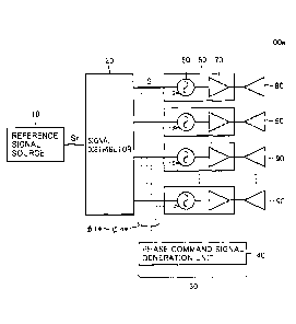
Fig. 1 is a block diagram illustrating the configuration of an array antenna
device
100a configured to include a transmission module according to an embodiment of
the
present disclosure.
- 4 -
CA 02992120 2018-01-09
Referring to Fig. 1, array antenna device 100a includes a reference signal
source 10, a
signal distributor 20, a transmission module 30, and a plurality of element
antennas 90.
Transmission module 30 includes a phase command signal generator 40 and a
plurality of oscillator modules 50. In the present embodiment, transmission
module 30
is configured to include n (n: 2 or more natural numbers) oscillator modules
50. In total,
n element antennas 90 are provided so as to correspond to respective
oscillator modules
50.
Reference signal source 10 outputs a reference signal Sr. Reference signal Sr
corresponds, for example, to a reference clock of approximately several MHz to
several
hundred MHz. Signal distributor 20 branches reference signal Sr and transfers
the
branched signal to each of oscillator modules 50.
Each of oscillator modules 50 includes a voltage controlled oscillator 60 and
an
amplification circuit 70. Each of oscillator modules 50 outputs a transmission
signal
having a high frequency (for example, GHz order) (which will be hereinafter
also
referred to as a "transmission high-frequency signal"). The plurality of
element
antennas 90 are provided in an array arrangement so as to correspond to a
plurality of (n)
oscillator modules. Each of element antennas 90 is arranged so as to propagate
the
transmission high-frequency signal from a corresponding one of oscillator
modules 50
into space. Element antenna 90 corresponds to one embodiment of a "radiation
element".
To each of oscillator modules 50, a common reference signal Sr is transferred
through signal distributor 20. Voltage controlled oscillators 60 output
transmission
high-frequency signals having the same frequency under synchronous control
based on
reference signal Sr. Furthermore, in n oscillator modules 50, the phases of
the
transmission high-frequency signals from n voltage controlled oscillators 60
are
controlled according to respective phase command signals (p1* to (pn* from
phase
command signal generator 40. In the following description explaining the
configuration and the like common to n oscillator modules 50, phase command
signals
cp I* to cpn* are also collectively represented as a phase command signal (2*.
For example, by a PLL (Phase Locked Loop) receiving reference signal Sr as an
input signal, each of voltage controlled oscillators 60 performs synchronous
control so as
to output a high-frequency signal synchronized with reference signal Sr. In
this case, in
- 5 -
CA 02992120 2018-01-09
n oscillator modules 50, voltage controlled oscillators 60 output transmission
high-
frequency signals having the same frequency.
Furthermore, for each of the
transmission high-frequency signals, the phase difference relative to the
reference phase
given by reference signal Sr is controlled according to phase command signal
cp* for
each oscillator module 50. Accordingly, the relative phase among the n
transmission
high-frequency signals can be controlled freely in accordance with setting of
phase
command signals c 1* to cn*.
In each of oscillator modules 50, amplification circuit 70 amplifies a
transmission
high-frequency signal output from voltage controlled oscillator 60. The
transmission
high-frequency signal amplified by amplification circuit 70 is transferred to
element
antenna 90 as an output from oscillator module 50.
In array antenna device 100a, a plurality of (n) element antennas 90 transmit
transmission high-frequency signals from the plurality of (n) oscillator
modules 50
toward space. When the relative phase of the plurality of (n) transmission
high-
frequency signals is controlled by phase command signals c 1* to cn* from
phase
command signal generator 40, the shape and the direction of a transmission
beam from
each of the plurality of element antennas 90 can be freely controlled.
Thereby, array
antenna device 100a can output a transmission signal not employing a baseband
signal.
For example, array antenna device 100a can transmit a beam for a radar
application.
Fig. 2 shows the configuration of a commonly-used array antenna device 100#
shown as a comparative example.
Referring to Fig. 2, array antenna device 100# in a comparative example
includes
a voltage controlled oscillator 60, a signal distributor 65, a plurality of
oscillator modules
50#, a plurality of element antennas 90, and a phase command signal generator
40.
Also in array antenna device 1004, n oscillator modules 50# and n element
antennas 90 are provided. As in Fig. 1, phase command signal generator 40 also
generates phase command signals c 1* to cn* each used for controlling the
shape and the
direction of a transmission beam from a corresponding one of the plurality of
element
antennas 90.
Voltage controlled oscillator 60 outputs a transmission high-frequency signal.
Signal distributor 65 distributes a transmission high-frequency signal from
voltage
controlled oscillator 60 to each of the plurality of oscillator modules 50#.
Thereby,
- 6 -
CA 02992120 2018-01-09
each of the transmission high-frequency signals having the same frequency is
input into a
corresponding one of oscillator modules 50#, as a common signal.
Each of oscillator modules 50# includes a phase shifter 151, amplifiers 152
and
153. In each of n oscillator modules 50#, phase shifter 151 controls the phase
of the
input transmission high-frequency signal according to a corresponding one of
phase
command signals (p l* to (pn* from phase command signal generator 40, and
outputs the
controlled signal. As a result, n transmission high-frequency signals output
from n
phase shifters 151 have the same frequency and have phases separately
controlled
according to phase command signals (p 1* to (pn* in the same manner as with
the n
transmission high-frequency signals output from n voltage controlled
oscillators 60 in
Fig. 1.
In each of oscillator modules 50#, amplifiers 152 and 153 each amplify the
power
of the transmission high-frequency signal output from phase shifter 151, and
output the
amplified power to a corresponding element antenna 90. As a result, also in
array
antenna device 100# in the comparative example, n element antennas 90 can
output
transmission beams obtained by n transmission high-frequency signals as in
array
antenna device 100a (Fig. 1).
Array antenna device 100# in the comparative example is configured to input
each of transmission high-frequency signals having the same frequency into a
corresponding one of oscillator modules 50#, as a common signal. Accordingly,
signal
distributor 65 for distributing a high-frequency signal to each of oscillator
modules 50#
is increased in size, thereby also increasing power loss.
Furthermore, on the assumption that the power of the transmission high-
frequency signal output from voltage controlled oscillator 60 is defined as P,
the power
of the transmission high-frequency signal input into each of oscillator
modules 50# is
decreased to P/n. Thus, in each of oscillator modules 50#, the power
amplification
factor obtained by amplifiers 152 and 153 needs to be raised. Furthermore, in
each of
oscillator modules 50#, phase shifter 151 for phase control needs to be
arranged.
In contrast, in array antenna device 100a (Fig. 1) according to the first
embodiment, a reference signal that is lower in frequency than the
transmission high-
frequency signal is input in common into each of oscillator modules 50. Thus,
as
compared with signal distributor 65 in the comparative example, signal
distributor 20 is
- 7 -
CA 02992120 2018-01-09
simplified in configuration, and therefore, can be reduced in size. In
addition,
depending on the conditions of reference signal Sr, merely a wiring line
branching may
allow transmission of a common reference signal to each of oscillator modules
50. In
this case, arrangement of signal distributor 20 can be eliminated.
Furthermore, in each of oscillator modules 50, voltage controlled oscillator
60
outputs a transmission high-frequency signal. Accordingly, even if the power
of
reference signal Sr is decreased due to distribution, the power amplification
factor of the
transmission high-frequency signal is not influenced thereby. As a result, the
voltage
amplification factor obtained by amplification circuit 70 in oscillator module
50 can be
set smaller than the power amplification factor obtained by amplifiers 152 and
153 in
oscillator module 50#.
Furthermore, voltage controlled oscillators 60 are synchronously controlled
based
on common reference signal Sr as an input among n oscillator modules 50.
Accordingly, phase shifter 151 does not have to be provided as in oscillator
module 50#.
In this way, as compared with array antenna device 100# in the comparative
example, array antenna device 100a according to the first embodiment can be
configured
in such a manner that the power amplification factor is suppressed while the
number of
circuit elements is decreased in each of oscillator modules 50 configured to
output a
high-frequency signal for transmission not employing a baseband signal.
Furthermore,
since distribution of a high-frequency signal is not required at a stage
preceding each
oscillator module 50, a compact, low-cost and low-loss circuit configuration
can be
implemented. As a result, it becomes possible to implement a compact, low-cost
and
low-loss transmission module configuration that is suitable for transmission
by radar or
the like not employing a baseband signal.
Then, the configuration of oscillator module 50 in transmission module 30
according to the present embodiment will be hereinafter described in greater
detail.
Fig. 3 is a circuit diagram for illustrating a configuration example of
oscillator
module 50 shown in Fig. 1.
Referring to Fig. 3, oscillator module 50 includes power supply/control
circuitry
51, a voltage controlled oscillator 60, and an amplification circuit 70. In
each oscillator
module 50, power supply/control circuitry 51 is represented collectively as
one block
including a power supply circuit for supplying electric power to each
component element
- 8 -
CA 02992120 2018-01-09
and a control circuit for generating a control command signal for each
component
element.
Voltage controlled oscillator 60 operates with electric power received from
power supply/control circuitry 51. Voltage controlled oscillator 60 receives
an input of
a reference signal Sr that is output from reference signal source 10 and
distributed by
signal distributor 20. This reference signal Sr is common among n oscillator
modules
50 shown in Fig. 1.
Voltage controlled oscillator 60 outputs a transmission high-frequency signal
that
is controlled in synchronization with reference signal Sr by PLL or the like.
As
described above, the phase of the transmission high-frequency signal is
controlled
according to a phase command signal 9* for each oscillator module 50.
Amplification circuit 70 includes amplifiers 72a and 72b arranged in series, a
distribution circuit 74, a plurality of amplifiers 72c arranged in parallel, a
combining
circuit 75, and an isolator 77. Amplifiers 72a, 72b and a plurality of
amplifiers 72c
operate with the electric power from power supply/control circuitry 51.
Each of amplifiers 72a and 72b performs power amplification for a transmission
high-frequency signal output from voltage controlled oscillator 60.
Distribution circuit
74 distributes the output signal of amplifier 72b to the plurality of
amplifiers 72c. Each
of amplifiers 72c performs power amplification for the transmission high-
frequency
signal input from distribution circuit 74 and outputs the resultant signal.
Combining
circuit 75 combines the transmission high-frequency signals output from the
plurality of
amplifiers 72c. Distribution circuit 74 and combining circuit 75 can be
formed, for
example, using a 90-degree hybrid circuit.
As in the configuration example in Fig. 3, power amplification is performed by
the plurality of amplifiers 72c using distribution circuit 74 and combining
circuit 75, so
that the output power can be readily secured. Accordingly, when the
transmission high-
frequency signal does not need to have much output power, arrangement of
distribution
circuit 74 and combining circuit 75 may be eliminated and only a single
amplifier 72c
may be arranged. Furthermore, amplifiers 72a and 72b can also be formed by a
one-
stage amplifier.
Isolator 77 is provided for protecting amplifier 72c from excessive output
reflection from element antenna 90. In addition, isolator 77 can also be
configured in
- 9 -
CA 02992120 2018-01-09
such a manner that a plurality of isolators each having small withstand power
are
arranged in intermediate stages of combining power in combining circuit 75.
Oscillator module 50 is separated into two circuit blocks CKa and CKb during
mounting. Circuit block CKa includes a voltage controlled oscillator 60 and
power
supply/control circuitry 51. Furthermore, one of amplifiers 72a and 72b (for
example,
amplifier 72a) can be arranged so as to be included in circuit block CKa. In
the
configuration example in Fig. 3, amplifier 72a of amplifiers 72a and 72b
provided in a
plurality of stages is included in circuit block CKa. This circuit block CKa
is provided
with: components in a circuit portion including a large number of control
wiring lines for
PLL; and components in a relatively small power portion.
On the other hand, circuit block CKb includes at least one of amplifiers 72a
and
72b (for example, amplifier 72b), a distribution circuit 74, an amplifier 72c,
a combining
circuit 75, and an isolator 77. Circuit block CKb includes a component having
a
relatively high power portion and, due to its significant heat generation,
requiring a heat
radiation structure.
Fig. 4 shows a perspective view for illustrating a mounting example of
oscillator
module 50 whose components are categorized into circuit blocks CKa and CKb.
Referring to Fig. 4, oscillator module 50 is implemented in a two-story
structure
obtained by stacking, as an integrated substrate, a substrate 207 having
circuit block CKa
mounted thereon and a substrate 210 having circuit block CKb mounted thereon.
Substrate 207 having circuit block CKa mounted thereon is fabricated as a
substrate integrally provided with high-frequency signal circuitry dealing
with a small
signal, such as power supply/control circuitry 51, voltage controlled
oscillator 60
including a large number of control wiring lines due to being PLL-controlled,
amplifier
72a in the first stage, and the like. Thereby, size reduction and wiring-line
connection
are facilitated.
Since substrate 210 having circuit block CKb mounted thereon is provided with
a
circuit element causing significant heat generation due to high output power,
this
substrate 210 requires a heat radiation structure. Thus, substrate 210 is
arranged in the
first-floor portion of the structure. Furthermore, substrate 210 is arranged
on a metal
base 202 to which a heat radiation fin 201 is attached. Thereby, the heat
generated
from the circuit elements included in circuit block CKb can be dissipated from
heat
radiation fin 201. In this case, when heat radiation fin 201 is configured in
a separable
- 10 -
CA 02992120 2018-01-09
structure, the cooling method can be changed into a water-cooling method or
the like as
required.
Substrate 210 mounted on metal base 202 is covered by an input-side connector
plate 203 and an output-side connector plate 204 that are made of metal and a
metal plate
206. Furthermore, a longitudinal wall formed of a sponge 211 having
conductivity is
provided on a GND pattern of substrate 210.
Thereby, the shield structure for inter-element isolation that is required
between
circuit block CKa (a substrate 207) and circuit elements on circuit block CKb
emitting
large output power is implemented by (i) the longitudinal wall formed of
sponge 211 and
(ii) input-side connector plate 203, output-side connector plate 204 and metal
plate 206
for covering the structure in the first floor portion. In other words, the
longitudinal wall
formed of sponge 211 is formed so as to have a height required for isolation
along the
direction in which substrates 210 and 207 are stacked.
By providing such a shield structure, the engraved structure of metal base 202
can be simplified. Furthermore, in any portion where a GND pattern is provided
on
substrate 210, the shape and the size of the space that needs to be shielded
can be
flexibly changed.
In addition, input-side connector plate 203 and output-side connector plate
204
are not only configured to have a shield structure but also provided with a
connector
serving as an input/output interface from the outside. Specifically, input-
side connector
plate 203 is provided with a connector 203a for receiving an input of
reference signal Sr.
Output-side connector plate 204 is provided with a connector 204a for
outputting a
transmission high-frequency signal to element antenna 90.
Circuit elements (circuit block CKa) mounted on substrate 207 and circuit
elements (circuit block CKb) mounted on substrate 210 are connected via a
wiring line
passing through each hole that is provided in metal plate 206 and that has a
size not
influencing isolation. In this case, a covered wire is used for a wiring line
through
which a power supply and a control signal are transmitted. On the other hand,
it is
preferable that a coaxial wire is used for a wiring line through which a high-
frequency
signal is transmitted.
The circuit structure (two-story structure) of oscillator module 50 formed on
metal base 202 is covered by a metal cover 208. Metal cover 208 is attached as
an
-11-
CA 02992120 2018-01-09
isolation structure for circuit block CKa in addition to the purpose of
protecting the
circuit structure from the impact and the like received from outside.
According to the example of the mounting structure in Fig. 4, each oscillator
module 50 forming the transmission module according to the first embodiment
can be
efficiently mounted. In the example in Fig. 4, substrate 210 corresponds to
the "first
substrate" and substrate 207 corresponds to the "second substrate".
(Modification of Configuration of Oscillator Module)
Fig. 5 is a circuit diagram illustrating the configuration of an oscillator
module
50a in the first modification.
When comparing Fig. 5 with Fig. 3, oscillator module 50a according to the
first
modification is different from the configuration of oscillator module 50 (Fig.
3)
according to the first embodiment in that this oscillator module 50a further
includes a
variable gain amplifier 71, an output power monitor circuit 78 and a reflected
power
monitor circuit 79. Since other configurations of oscillator module 50a are
the same as
those of oscillator module 50, the detailed description thereof will not be
repeated.
Variable gain amplifier 71 is arranged between voltage controlled oscillator
60
and amplifier 72a. Variable gain amplifier 71 operates with the power supply
received
from power supply/control circuitry 51, to perform power amplification for the
transmission high-frequency signal from voltage controlled oscillator 60 and
output the
resultant signal. The power amplification factor equivalent to the power ratio
between
the input signal and the output signal of variable gain amplifier 71 changes
in accordance
with the control signal from power supply/control circuitry 51.
In each oscillator module 50a, output power monitor circuit 78 measures the
output power of the transmission high-frequency signal from amplification
circuit 70.
Reflected power monitor circuit 79 measures the reflected power from element
antenna
90. The output power detected by output power monitor circuit 78 and the
reflected
power detected by reflected power monitor circuit 79 are input into power
supply/control
circuitry 51.
For example, output power monitor circuit 78 and reflected power monitor
circuit
79 can be configured to extract a part of the output power and a part of the
reflected
power, respectively, using a directional coupler, and also configured to
detect the
extracted power using a wave detector.
- 12 -
CA 02992120 2018-01-09
Power supply/control circuitry 51 controls the power amplification factor of
variable gain amplifier 71 based on at least one of the output power and the
reflected
power measured by output power monitor circuit 78 and reflected power monitor
circuit
79, respectively.
For example, the voltage amplification factor obtained by variable gain
amplifier
71 can be controlled such that the output power measured by output power
monitor
circuit 78 becomes equal to predetermined reference power. In this way, the
output
power of the transmission high-frequency signal from each oscillator module
50a can be
precisely controlled according to the reference power suitable for forming
various beams
output from array antenna device 100. Alternatively, also in the environment
in which
a temperature changes, it becomes possible to compensate the change in output
power of
voltage controlled oscillator 60 and the change in gains of amplifiers 72a to
72c that are
caused by the temperature dependency, so that the output power of the
transmission
high-frequency signal from oscillator module 50a can be maintained constant.
Furthermore, for the purpose of equipment protection control during occurrence
of abnormalities, when at least one of the output power and the reflected
power measured
by output power monitor circuit 78 and reflected power monitor circuit 79 is
higher than
a predetermined threshold value, the power amplification factor of variable
gain
amplifier 71 is set to be 0 and the output of the transmission high-frequency
signal is
stopped, thereby allowing protection of oscillator module 50a against
failures.
Fig. 6 is a circuit diagram illustrating the configuration of an oscillator
module
50b in the second modification.
When comparing Fig. 6 with Fig. 5, oscillator module 50b according to the
second modification is different from oscillator module 50a (Fig. 5) in that
this oscillator
module 50b includes a variable attenuator 81 in place of variable gain
amplifier 71.
Variable attenuator 81 operates with the power supply received from power
supply/control circuitry 51 to attenuate the power of the transmission high-
frequency
signal from voltage controlled oscillator 60. The power attenuation factor
equivalent to
the power ratio between the input signal and the output signal of variable
attenuator 81
changes in accordance with the control signal from power supply/control
circuitry 51.
Since other configurations of oscillator module 50b are common to those of
oscillator
module 50a, the detailed description thereof will not be repeated.
- 13 -
CA 02992120 2018-01-09
In oscillator module 50b, the power attenuation factor in variable attenuator
81
can be controlled in accordance with the monitoring results obtained by output
power
monitor circuit 78 and reflected power monitor circuit 79 in the same manner
as with the
power amplification factor of variable gain amplifier 71 in oscillator module
50a.
Accordingly, also in oscillator module 50b, the output power of the
transmission high-
frequency signal can be maintained at predetermined reference power.
Alternatively,
when the output power and/or the reflected power exceeds a threshold value,
the power
attenuation factor in variable attenuator 81 is set to be infinite, and the
output of the
transmission high-frequency signal from oscillator module 50b is stopped,
thereby
allowing execution of equipment protection control.
In this way, according to oscillator modules 50a and 50b in the modifications
shown in Figs. 6 and 7, variable gain amplifier 71 or variable attenuator 81
is further
arranged, thereby allowing execution of precise control for the output power
of the
transmission high-frequency signal and also allowing equipment protection
control under
the excessive output power and reflected power. In the configurations in Figs.
6 and 7,
each of variable gain amplifier 71 and variable attenuator 81 corresponds to
one
embodiment of the "power regulator", and each of output power monitor circuit
78 and
reflected power monitor circuit 79 corresponds to one embodiment of the
"detector".
In addition, oscillator modules 50a and 50b according to the modifications
shown
in Figs. 6 and 7 can also be configured according to the example of the
mounting
structure illustrated in Fig. 4. In this case, variable gain amplifier 71 and
variable
attenuator 81 are configured to amplify or attenuate the transmission high-
frequency
signal of relatively small electric power from voltage controlled oscillator
60 according
to the control signal from power supply/control circuitry 51. Accordingly, it
is
preferable that such variable gain amplifier 71 and variable attenuator 81 are
mounted on
substrate 207 as circuit elements in circuit block CKa. On the other hand,
output power
monitor circuit 78 and reflected power monitor circuit 79 are configured to
measure a
relatively large electric power on the output side of amplification circuit
70.
Accordingly, it is preferable that such output power monitor circuit 78 and
reflected
power monitor circuit 79 are mounted on substrate 210 as circuit elements in
circuit
block CKb.
Modification of First Embodiment
- 14 -
CA 02992120 2018-01-09
Fig. 7 is a block diagram showing the configuration of an array antenna device
100b according to a modification of the first embodiment of the present
disclosure.
When comparing Fig. 7 with Fig. 1, array antenna device 100b according to the
modification of the first embodiment is different from array antenna device
100a (Fig. 1)
according to the first embodiment in that this array antenna device 100b
includes a
waveguide 91 and a horn antenna 92 as an element antenna 90. Since other
configurations of array antenna device 100b are the same as those of array
antenna
device 100a, the detailed description thereof will not be repeated.
In addition, as a plurality of oscillator modules included in transmission
module
30, array antenna device 100b also can employ the configuration of oscillator
module
50a shown in Fig. 5 or oscillator module 50b shown in Fig. 6 in addition to
the
configuration of oscillator module 50 shown in Fig. 3.
In this way, even if the element antenna is formed of a horn antenna,
transmission
module 30 suitable for transmission not employing a baseband signal is used to
output,
from array antenna device 100b, a plurality of transmission high-frequency
signals
having the same frequency and having phases that are controlled independently
from
each other, so that a transmission beam can be formed.
Second Embodiment
In the first embodiment, an explanation has been given with regard to the
configuration of the array antenna device for controlling a transmission beam
by
performing, in space, power combining of transmission high-frequency signals
from the
transmission modules according to the embodiment of the present disclosure.
However,
the transmission module according to the embodiment of the present disclosure
can be
applied not only to a spatial combining scheme but also to a high-power
transmission
device configured to perform power combining using a power combiner.
Fig. 8 is a block diagram illustrating the configuration of a transmission
device
110 according to the second embodiment, which is formed by including a
transmission
module according to an embodiment of the present disclosure.
Referring to Fig. 8, transmission device 110 according to the second
embodiment
includes a reference signal source 10, a signal distributor 20 and a
transmission module
30 as in array antenna device 100a shown in Fig. 1. Furthermore, transmission
device
110 includes a power combiner 80.
- 15 -
CA 02992120 2018-01-09
Transmission module 30, which is configured in a manner similar to the first
embodiment, includes a plurality of (n) oscillator modules 50.
Alternatively,
transmission module 30 may be formed using oscillator module 50a (Fig. 5) or
oscillator
module 50b (Fig. 6) in place of oscillator module 50.
Unlike array antenna device 100, transmission device 110 is provided with
power
combiner 80 in place of n element antennas 90.
Power combiner 80 performs power combining of the outputs from n oscillator
modules 50 (50a, 50b) to generate a transmission signal from transmission
device 110.
It is known that the output power from power combiner 80 reaches a maximum
level
when the phase condition among the input signals is optimized. Accordingly,
when
transmission module 30 is applied to transmission device 110, phase command
signal
generator 40 generates phase command signals 91* to (pn* such that the phase
relation
among the transmission high-frequency signals from n oscillator modules 50
(50a, 50b)
is optimized at an input terminal of power combiner 80.
For example, when the output power from power combiner 80 is maximized
when the in-phase signal is input, phase control command signals 91* to cpn*
can be
regulated such that n transmission high-frequency signals are actually aligned
in phase at
the input terminal of power combiner 80.
In this way, according to the transmission device in the second embodiment,
transmission module 30 according to the present embodiment including
oscillator
module 50 (50a, 50b) is used to perform phase regulation at the input terminal
of power
combiner 80. Thereby, a transmission signal not including a baseband signal
can be
achieved at high output power by a compact, low-cost and low-loss circuit
configuration.
Particularly, when the output power can be precisely controlled by applying
oscillator modules 50a and 50b, an initial regulation of the reference power
of the output
from each of oscillator modules 50a and 50b can be carried out such that
transmission
high-frequency signals at the input terminal of power combiner 80 are
equalized in
amplitude. Thereby, the output power from power combiner 80 can be maximized,
so
that the transmission signal can be achieved at higher output power.
Third Embodiment
- 16 -
CA 02992120 2018-01-09
In the third embodiment, an explanation will be given with regard to the
configuration in which the output power of each voltage controlled oscillator
60 can be
controlled in each transmission module 30.
Fig. 9 is a block diagram illustrating the configuration of an array antenna
device
101 including a transmission module according to the third embodiment.
When comparing Fig. 9 with Fig. I, array antenna device 101 according to the
third embodiment is different from array antenna device 100 according to the
first
embodiment in that this array antenna device 101 includes a transmission
module 31 in
place of transmission module 30. Transmission module 31 is different from
transmission module 30 in that it further includes an amplitude command signal
generator 41.
Amplitude command signal generator 41 generates amplitude command signals
Al* to An* for voltage controlled oscillators 60 to n oscillator modules 50.
Amplitude
command signals A I* to An* are input into respective voltage controlled
oscillators 60
in n oscillator modules 50.
In each of n oscillator modules 50, voltage controlled oscillator 60 outputs a
transmission high-frequency signal having an amplitude in accordance with
amplitude
command signal A*(collectively representing Al* to An*). Thereby, the output
power
of the transmission high-frequency signal from each of voltage controlled
oscillators 60
can be controlled separately in a corresponding one of n oscillator modules
50.
Since the configuration and the operation in each portion other than the above
in
array antenna device 101 are the same as those in array antenna device 100
(Fig. 1), the
detailed description thereof will not be repeated.
In the array antenna device, when each element antenna 90 outputs equal output
power, a side lobe may be increased in size. In such a case, when the output
power
from each of n oscillator modules 50 is intentionally changed in strength, the
side lobe
can be improved. For example, when the side lobe is improved by an amplitude
distribution pattern in which the amplitude of the transmission high-frequency
signal
from element antenna 90 in the center portion is stronger than the amplitude
of the
transmission high-frequency signal from element antenna 90 in the peripheral
portion,
amplitude command signals Al* to An* can be set according to this amplitude
pattern.
- 17 -
CA 02992120 2018-01-09
Thereby, according to the array antenna device in the third embodiment, a
transmission beam with a small side lobe can be output by conducting separate
control of
the output power from voltage controlled oscillator 60 in each of oscillator
modules 50.
Also in oscillator modules 50a and 50b shown in Fig. 5 and Fig. 6, the
reference
power in feedback control using the measured value obtained by output power
monitor
circuit 78 is set separately in n oscillator modules 50a and 50b in accordance
with the
above-mentioned amplitude pattern. Thereby, a transmission beam with a small
side
lobe can be similarly output. Conversely, in the configuration of the third
embodiment,
a transmission beam with a small side lobe can be output without having to
arrange
variable gain amplifier 71 or variable attenuator 81.
Fig. 10 is a block diagram illustrating the configuration of a transmission
device
111 including a transmission module according to the third embodiment.
When comparing Fig. 10 with Fig. 8, transmission device 111 according to the
third embodiment is different from transmission device 110 according to the
second
embodiment in that this transmission device 111 includes a transmission module
31 in
place of transmission module 30.
Transmission module 31 is different from
transmission module 30 in that this transmission module 31 further includes an
amplitude command signal generator 41 as in Fig. 9. The output power of the
transmission high-frequency signal from each of voltage controlled oscillators
60 can be
controlled separately in a corresponding one of n oscillator modules 50.
Since the configuration and the operation in each portion other than the above
in
transmission device 111 are the same as those in transmission device 110 (Fig.
8), the
detailed description thereof will not be repeated.
As described above, in the transmission device configured to generate a
transmission signal by power combining, amplitude command signals Al* to An*
can be
regulated such that the transmission high-frequency signals from oscillator
modules 50
are actually equalized in amplitude at the input terminal of power combiner
80.
Thereby, according to the transmission device in the third embodiment, the
power
of the transmission signal output from power combiner 80 can be maximized.
Particularly, a transmission signal can be achieved at high output power using
oscillator
module 50 having a simple configuration without using oscillator modules 50a
and 50b
provided with variable gain amplifier 71 and variable attenuator 81,
respectively.
- 18-
CA 02992120 2018-01-09
It should be understood that the embodiments disclosed herein are illustrative
and
non-restrictive in every respect. The scope of the present disclosure is
defined by the
terms of the claims, rather than the description above, and is intended to
include any
modifications within the meaning and scope equivalent to the terms of the
claims.
Reference Signs List
reference signal source, 20, 65 signal distributor, 30, 31 transmission
module,
40 phase command signal generator, 41 amplitude command signal generator, 50,
50a,
50b, 50# oscillator module, 51 power supply/control circuitry, 60 voltage
controlled
oscillator, 70 amplification circuit, 71 variable gain amplifier, 72a, 72b,
72c, 152, 153
10 amplifier, 74 distribution circuit, 75 combining circuit, 77 isolator,
78 output power
monitor circuit, 79 reflected power monitor circuit, 80 power combiner, 81
variable
attenuator, 90 element antenna, 91 waveguide, 92 horn antenna, 100, 100a,
100b, 100#,
101 array antenna device, 110, 111 transmission device, 151 phase shifter, 201
heat
radiation fin, 202 metal base, 203 input-side connector plate 203a, 204a
connector, 204
output-side connector plate, 206 metal plate, 207, 210 substrate, 208 metal
cover, 211
sponge, A*, A1* to An* amplitude command signal, CKa, CKb circuit block, Sr
reference signal.
- 19 -