Note: Descriptions are shown in the official language in which they were submitted.
CA 02992276 2018-01-11
WO 2017/030683
PCT/US2016/041976
SWITCHED POWER CONTROL CIRCUITS FOR CONTROLLING THE
RATE OF PROVIDING VOLTAGES TO POWERED CIRCUITS, AND
RELATED SYSTEMS AND METHODS
PRIORITY APPLICATION
[0001] The
present application claims priority to U.S. Patent Application Serial No.
14/826,472, filed on August 14, 2015 and entitled "SWITCHED POWER CONTROL
CIRCUITS FOR CONTROLLING THE RATE OF PROVIDING VOLTAGES TO
POWERED CIRCUITS, AND RELATED SYSTEMS AND METHODS," which is
incorporated herein by reference in its entirety.
BACKGROUND
I. Field of the Disclosure
[0002] The
technology of the disclosure relates generally to controlling voltage slew
rates, and particularly to circuits that control the rate at which voltage is
supplied to a
load circuit.
Background
[0003]
Processor-based systems employ voltage supply sources for providing
voltage to various components for operation. Rather than coupling voltage
supply
sources directly to the components, a processor-based system may employ
headswitch
devices that distribute voltage from one or more voltage supply sources within
the
processor-based system. Notably, instead of continuously providing voltage to
components within the processor-based system, headswitch devices can be
provided and
configured to provide voltage to corresponding power distribution networks
within
these components during active operation. In this manner, power consumption of
a
processor-based system may be reduced when components are not operating.
[0004] For
example, to provide voltage to a processor core for powering the
processor core, multiple headswitch devices are commonly disposed at locations
on a
processing system die around a perimeter of the processor core. Distributing
the
placement of headswitch devices strategically at locations around the
perimeter of the
processing core allows a supply voltage to be provided to multiple areas of
the
processor core with less complex wiring, as compared to providing the supply
voltage
1
CA 02992276 2018-01-11
WO 2017/030683
PCT/US2016/041976
from a single node. In this manner, the headswitch devices are configured to
receive the
supply voltage from one or more voltage supply sources. To control the
distribution of
the supply voltage from the headswitch devices distributed on the processing
system
die, the headswitch devices are configured to be controlled by control
signals. The
control signals are provided from the processor core to activate the
headswitch devices
to supply power to the power distribution network of the processor core.
[0005]
However, prior to receiving the supply voltage from the headswitch devices,
the processor core may be in an idle state, wherein voltage provided to the
processor
core may be reduced or collapsed to reduce power consumption. Thus, the
voltage level
of the corresponding power distribution network within the processor core may
be
approximately equal to zero Volts (OV). However, when the processor core
transitions
from an idle state to an active state, the processor core sends a control
signal to the
headswitch devices to increase the voltage provided to the processor core.
Upon
receiving the supply voltage from the voltage supply sources by way of the
heads witch
devices, the voltage of the processor core is raised from a lower voltage to
the supply
voltage in a substantially instantaneous manner. This fast voltage step may
cause
prolonged resonance within the power distribution network of the processor
core.
Notably, a processor core cannot operate until resonance on the corresponding
power
distribution network subsides. However, delaying operation of a processor core
until
resonance on the power distribution network subsides reduces the performance
of the
processor core.
SUMMARY OF THE DISCLOSURE
[0006]
Aspects disclosed in the detailed description include switched power control
circuits for controlling the rate of providing voltages to powered circuits.
Related
systems and methods are also disclosed. In one aspect, a switched power
control circuit
is provided. The switched power control circuit is configured to control
activation of a
headswitch circuit such that the headswitch circuit gradually provides a
supply voltage
to a powered circuit. This is as opposed to providing the full supply voltage
in a
substantially instantaneous manner. To gradually provide the supply voltage,
an output
voltage is provided, wherein the output voltage is ramped up to the supply
voltage. To
gradually ramp up the output voltage provided by the headswitch circuit to the
powered
2
CA 02992276 2018-01-11
WO 2017/030683
PCT/US2016/041976
circuit, the headswitch circuit is configured to provide the output voltage
generated from
a voltage supply source to the powered circuit in response to a control signal
received
on a control input. The control signal is generated by a control circuit in
response to an
enable signal. To prevent the headswitch circuit from instantaneously
providing the full
supply voltage to the powered circuit, a current sink circuit is provided. The
current
sink circuit is configured to control a ramping rate of the output voltage
generated by
the headswitch circuit. Controlling the ramping rate corresponds to gradually
activating
the headswitch circuit over time, wherein the amount of supply voltage allowed
to pass
through the headswitch circuit is limited by the level of activation of the
headswitch
circuit. By using the switched power control circuit to gradually provide the
supply
voltage, the switched power control circuit may provide the supply voltage in
a
controlled manner, which may reduce or avoid prolonged resonance on a power
distribution network within the powered circuit. Because the powered circuit
delays
operation until such resonance subsides, using the switched power control
circuit to
reduce or avoid the resonance increases the perfointance of the powered
circuit.
[0007] In
this regard, in one aspect, a switched power control circuit is disclosed.
The switched power control circuit comprises a headswitch circuit. The
headswitch
circuit is configured to provide an output voltage generated from a voltage
supply
source to a powered circuit in response to a control signal received on a
control input.
The switched power control circuit further comprises a control circuit
configured to
generate the control signal to control the providing of the output voltage by
the
headswitch circuit to the powered circuit in response to an enable signal. The
switched
power control circuit further comprises a current sink circuit coupled to the
control
input, the current sink circuit configured to control a ramping rate of the
output voltage
generated by the headswitch circuit.
[0008] In
another aspect, a switched power control circuit is disclosed. The
switched power control circuit comprises a means for providing an output
voltage
generated from a voltage supply source to a powered circuit in response to a
control
signal received on a control input. The switched power control circuit further
comprises
a means for generating the control signal to control the providing of the
output voltage
by the means for providing the output voltage to the powered circuit. The
switched
power control circuit further comprises a means for controlling a ramping rate
of the
3
84143412
output voltage generated by the means for providing the output voltage to the
powered circuit.
[0009] In another aspect, a method for gradually providing a supply
voltage to a powered
circuit is disclosed. The method comprises generating a control signal to
control providing of an
output voltage generated from a voltage supply source by a headswitch circuit
to a powered
circuit in response to an enable signal. The method further comprises
controlling a ramping rate
of the output voltage generated by the headswitch circuit by a current sink
circuit coupled to a
control input of the headswitch circuit. The method further comprises
providing the output
voltage to the powered circuit from the headswitch circuit in response to the
control signal
received on the control input.
[0010] In another aspect, a block headswitch system is disclosed. The
block headswitch
system comprises a plurality of switched power control circuits. Each switched
power control
circuit comprises an enable input configured to receive an enable signal. Each
switched power
control circuit further comprises an enable output configured to provide the
enable signal. Each
switched power control circuit further comprises a headswitch circuit
configured to provide an
output voltage generated from a voltage supply source to a powered circuit in
response to a
control signal received on a control input. Each switched power control
circuit further comprises
a control circuit configured to generate the control signal to control the
providing of the output
voltage by the headswitch circuit to the powered circuit in response to the
enable signal. Each
switched power control circuit further comprises a current sink circuit
coupled to the control
input. The current sink circuit is configured to control a ramping rate of the
output voltage
generated by the headswitch circuit.
[0010a] According to one aspect of the present invention, there is
provided a switched
power control circuit, comprising: a headswitch circuit configured to provide
an output voltage
generated from a voltage supply source to a powered circuit in response to a
control signal
received on a control input; a control circuit configured to generate the
control signal to
control providing of the output voltage by the headswitch circuit to the
powered circuit in
response to an enable signal; a current sink circuit coupled to the control
input, the current
sink circuit configured to control a ramping rate of the output voltage
generated by the
headswitch circuit; a second enable input configured to receive a second
enable signal; and a
buffer configured to: receive the second enable signal; and provide the second
enable signal to
the headswitch circuit; wherein the buffer is activated in response to
deactivation of the enable
signal; and wherein the headswitch circuit is further configured to provide a
supply voltage
4
Date Recue/Date Received 2022-12-09
84143412
of the voltage supply source to the powered circuit in a substantially
instantaneous manner in
response to the second enable signal.
[0010b] According to another aspect of the present invention, there is
provided a switched
power control circuit, comprising: a means for providing an output voltage
generated from a
voltage supply source to a powered circuit in response to a control signal
received on a control
input; a means for generating the control signal to control providing of the
output voltage by the
means for providing the output voltage to the powered circuit in response to
an enable signal; a
means for controlling a ramping rate of the output voltage generated by the
means for providing
the output voltage to the powered circuit; a means for receiving a second
enable signal; and a
means for buffering the second enable signal configured to provide the second
enable signal to
the means for providing the output voltage; wherein the means for buffering
the second enable
signal is activated in response to deactivation of the enable signal; and
wherein the means for
providing the output voltage is configured to provide a supply voltage of the
voltage supply
source to the powered circuit in a substantially instantaneous manner in
response to the second
enable signal.
10010c] According to still another aspect of the present invention,
there is provided a
method for gradually providing a supply voltage to a powered circuit,
comprising: generating a
control signal to control providing of an output voltage generated from a
voltage supply source
by a headswitch circuit to the powered circuit in response to an enable
signal; controlling a
ramping rate of the output voltage generated by the headswitch circuit by a
current sink circuit
coupled to a control input of the headswitch circuit; providing the output
voltage to the powered
circuit from the headswitch circuit in response to the control signal received
on the control
input; receiving a second enable signal; buffering the second enable signal,
wherein the
second enable signal is provided to the headswitch circuit in response to
deactivation of the
enable signal; and providing the supply voltage of the voltage supply source
to the powered
circuit in a substantially instantaneous manner in response to the second
enable signal.
[0010d] According to yet another aspect of the present invention, there
is provided a block
headswitch system, comprising: a plurality of switched power control circuits,
each switched
power control circuit comprising: an enable input configured to receive an
enable signal; an
enable output configured to provide the enable signal; a headswitch circuit
configured to provide
an output voltage generated from a voltage supply source to a powered circuit
in response to a
control signal received on a control input; a control circuit configured to
generate the control
signal to control providing of the output voltage by the headswitch circuit to
the powered circuit
4a
Date Regue/Date Received 2022-12-09
84143412
in response to the enable signal; a current sink circuit coupled to the
control input, the current
sink circuit configured to control a ramping rate of the output voltage
generated by the
headswitch circuit; a second enable input configured to receive a second
enable signal; a second
enable output configured to provide the second enable signal; and a buffer
configured to: receive
the second enable signal; and provide the second enable signal to the
headswitch circuit; wherein
the buffer is activated in response to deactivation of the enable signal; and
wherein the
headswitch circuit is further configured to provide a supply voltage of the
voltage supply source
to the powered circuit in a substantially instantaneous manner in response to
receiving the
second enable signal.
BRIEF DESCRIPTION OF THE FIGURES
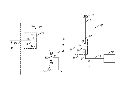
[0011] Figure 1 is a circuit diagram of an exemplary switched power
control circuit
configured to gradually provide a supply voltage to a powered circuit to
reduce or avoid
resonance in the powered circuit, and thus increase performance;
[0012] Figure 2 is a flowchart illustrating an exemplary process for
gradually providing
the supply voltage to the powered circuit in Figure 1 to reduce or avoid
resonance in the powered
circuit;
4h
Date Regue/Date Received 2022-12-09
CA 02992276 2018-01-11
WO 2017/030683
PCT/US2016/041976
[0013] Figure
3 is a graph illustrating that the supply voltage provided by the
switched power control circuit in Figure 1 is provided gradually over time;
[0014] Figure
4 is a circuit diagram of an exemplary switched power control circuit
configured to gradually provide a supply voltage to a powered circuit to
reduce or avoid
resonance in the powered circuit, wherein a ramping rate of an output voltage
is
controlled by a bias generator circuit;
[0015] Figure
5 is a block diagram of an exemplary block headswitch system
configured to gradually provide a supply voltage to a processor core to reduce
or avoid
resonance on a power distribution network within the processor core;
[0016] Figure
6 is a circuit diagram of another exemplary switched power control
circuit configured to gradually provide a supply voltage to a powered circuit
to reduce
or avoid resonance in the powered circuit, and thus increase performance;
[0017] Figure
7 is a block diagram of another exemplary block headswitch system
configured to gradually provide a supply voltage to a processor core to reduce
or avoid
resonance on a power distribution network within the processor core;
[0018] Figure
8 is a graph illustrating that voltage slew rates resulting from the
switched power control circuit in Figure 4 are approximately equal across
various levels
of load current;
[0019] Figure
9 is a graph illustrating that voltage slew rates resulting from the
switched power control circuit in Figure 4 are approximately equal across
various levels
of load capacitance of the powered circuit;
[0020] Figure
10 is a graph illustrating voltage slew rates generated when a bias
generator is used to bias the switched power control circuit in Figure 4;
[0021] Figure
11 is a block diagram illustrating a system wherein block headswitch
systems are distributed around a processor core, and wherein the block
headswitch
systems are configured to gradually provide a supply voltage to the processor
core; and
[0022] Figure
12 is a block diagram of an exemplary processor-based system that
can include the switched power control circuits of Figures 1 and 4 configured
to
gradually provide a supply voltage to a powered circuit to reduce or avoid
resonance in
the powered circuit.
CA 02992276 2018-01-11
WO 2017/030683
PCT/US2016/041976
DETAILED DESCRIPTION
[0023] With
reference now to the drawing figures, several exemplary aspects of the
present disclosure are described. The word "exemplary" is used herein to mean
"serving as an example, instance, or illustration." Any aspect described
herein as
"exemplary" is not necessarily to be construed as preferred or advantageous
over other
aspects.
[0024] Figure
1 illustrates an exemplary switched power control circuit 100
configured to gradually provide a supply voltage (VDD) from a voltage supply
source
102 to a powered circuit 104. To gradually provide the supply voltage (VDD),
an output
voltage (V) is provided, wherein the output voltage (V) is ramped up to the
supply
voltage (VDD). By gradually providing the supply voltage (VDD) to the powered
circuit
104, the switched power control circuit 100 may provide the supply voltage
(VDD) in a
controlled manner, which may reduce or avoid resonance in a power distribution
network (PDN) (not shown) of the powered circuit 104, thus increasing the
performance
of the powered circuit 104. To achieve this gradual ramping up of the output
voltage
(V), the switched power control circuit 100 employs a headswitch circuit 106
that is
configured to provide the output voltage (V) generated from the voltage supply
source
102 to the powered circuit 104. The headswitch circuit 106 includes a voltage
input 108
that is coupled to a voltage input 110 of the switched power control circuit
100 and
configured to receive the supply voltage (VDD) generated by the voltage supply
source
102. The headswitch circuit 106 also includes a voltage output 112 that is
coupled to a
voltage output 114 of the switched power control circuit 100 and configured to
provide
the output voltage (V) to the powered circuit 104. The headswitch circuit 106
is
configured to provide the output voltage (V) to the powered circuit 104 in
response to a
control signal 116 received on a control input 118. The control signal 116 is
generated
by a control circuit 120 in response to an enable signal 122. The switched
power
control circuit 100 also includes a current sink circuit 124 configured to
control a
ramping rate of the output voltage (V) generated by the headswitch circuit
106, thus
allowing the headswitch circuit 106 to provide the full supply voltage (VDD)
to the
powered circuit 104 in a controlled manner to reduce or avoid resonance in the
PDN of
the powered circuit 104. Controlling the ramping rate corresponds to gradually
activating (i.e., gradually turning-on) the headswitch circuit 106 over time,
wherein the
6
CA 02992276 2018-01-11
WO 2017/030683
PCT/US2016/041976
amount of supply voltage (VDD) allowed across the headswitch circuit 106 is
limited by
its level of activation.
[0025] With
continuing reference to Figure 1, in this aspect, the headswitch circuit
106 is controlled by the current sink circuit 124 when the control circuit 120
generates
the control signal 116 in response to the enable signal 122 received on an
enable input
126 of the switched power control circuit 100. The control signal 116
indicates that the
supply voltage (VDD) is to be transferred from the voltage supply source 102
to the
powered circuit 104. By using the switched power control circuit 100 to
gradually
provide the supply voltage (VDD) in a controlled manner, the switched power
control
circuit 100 reduces or avoids prolonged resonance on the power distribution
network
within the powered circuit 104. Because the powered circuit 104 delays
operation until
such resonance subsides, using the switched power control circuit 100 to
reduce or
avoid this resonance increases the performance of the powered circuit 104.
[0026] With
continuing reference to Figure 1, components within the switched
power control circuit 100 may employ various circuit elements to achieve the
functionality described above. In this aspect, the headswitch circuit 106
employs a p-
type metal oxide semiconductor (PMOS) transistor 128. The PMOS transistor 128
includes a source (S) that is coupled to the voltage input 108, a gate (G)
that is coupled
to the control input 116, and a drain (D) that is coupled to the voltage
output 112.
Additionally, in this aspect, the current sink circuit 124 includes an n-type
metal oxide
semiconductor (NMOS) transistor 130. The NMOS transistor 130 includes a source
(S)
that is coupled to a ground source 132, a drain (D) that is coupled to the
gate (G) of the
PMOS transistor 128 of the headswitch circuit 106 (i.e., the control input
118), and a
gate (G). The gate (G) of the NMOS transistor 130 in this aspect is driven by
a constant
voltage source 134. The
control circuit 120 in this example employs a PMOS
transistor 136. The PMOS transistor 136 includes a source (S) that is coupled
to the
voltage supply source 102, a gate (G) that is configured to receive the enable
signal 122,
and a drain (D) that is coupled to the gate (G) of the PMOS transistor 128 of
the
headswitch circuit 106 and the drain (D) of the NMOS transistor 130 of the
current sink
circuit 124. Notably, other aspects may employ coupling the source (S) of the
PMOS
transistor 136 to a voltage supply source other than the voltage supply source
102.
7
CA 02992276 2018-01-11
WO 2017/030683
PCT/US2016/041976
[0027] With
continuing reference to Figure 1, the functionality of the switched
power control circuit 100 is now described in detail. Because the enable
signal 122 is
coupled to the gate (G) of the PMOS transistor 136 of the control circuit 120,
the PMOS
transistor 136 is activated (i.e., turned-on) while the enable signal 122 has
a logic low
'0' value. Further, the supply voltage (VDD) from the voltage supply source
102 is
provided to the gate (G) of the PMOS transistor 128 of the headswitch circuit
106 while
the PMOS transistor 136 is activated. Providing the supply voltage (VDD) to
the gate
(G) of the PMOS transistor 128 deactivates (i.e., turns-off) the PMOS
transistor 128 and
prevents the supply voltage (VDD) from being provided to the powered circuit
104.
[0028] In
response to the enable signal 122 transitioning to a logic high '1' value,
the PMOS transistor 136 of the control circuit 120 is deactivated, which
prevents the
supply voltage (VDD) of the voltage supply source 102 from being provided to
the gate
(G) of the PMOS transistor 128 of the headswitch circuit 106. However,
although the
gate (G) of the PMOS transistor 128 is no longer receiving the supply voltage
(VDD)
from the voltage supply source 102, the supply voltage (VDD) remains on the
gate (G) of
the PMOS transistor 128, as a gate capacitance associated with the gate (G) of
the
PMOS transistor 128 is charged with the supply voltage (VDD) while the enable
signal
122 has a logic low value '0'.
[0029] With
continuing reference to Figure 1, because the supply voltage (VDD)
provided by the control circuit 120 no longer deactivates the PMOS transistor
128 of the
headswitch circuit 106, the PMOS transistor 128 may be activated so as to
provide the
output voltage (V) generated from the voltage supply source 102 to the powered
circuit
104. However, rather than fully activating the PMOS transistor 128 in a
substantially
instantaneous manner, the current sink circuit 124 is configured to gradually
activate the
PMOS transistor 128 over time such that the output voltage (V) provided by the
headswitch circuit 106 ramps up over time. The gate (G) of the NMOS transistor
130 of
the current sink circuit 124 is driven by the constant voltage source 134 in
this example
so as to activate the NMOS transistor 130 to a level that causes the voltage
on the gate
(G) of the PMOS transistor 128 of the headswitch circuit 106 to gradually
discharge
through the NMOS transistor 130 to the ground source 132.
[0030] With
continuing reference to Figure 1, as the voltage on the gate (G) of the
PMOS transistor 128 discharges, the PMOS transistor 128 gradually activates.
Notably,
8
CA 02992276 2018-01-11
WO 2017/030683
PCT/US2016/041976
the level of the output voltage (V) provided to the powered circuit 104 by the
headswitch circuit 106 corresponds to the level at which the PMOS transistor
128 is
activated. In other words, as the current sink circuit 124 discharges the
voltage on the
gate (G) of the PMOS transistor 128, the voltage on the gate (G) of the PMOS
transistor
128 crosses a threshold voltage (V1) of the PMOS transistor 128. As the
voltage on the
gate (G) of the PMOS transistor 128 crosses the threshold voltage (V,), the
PMOS
transistor 128 turns-on and provides a progressively higher output voltage (V)
to the
powered circuit 104. In this manner, the output voltage (V) provided to the
powered
circuit 104 gradually ramps up to the full supply voltage (VDD) as the voltage
on the
gate (G) of the PMOS transistor 128 crosses the threshold voltage (Vi). By
using the
switched power control circuit 100 to gradually provide the supply voltage
(VDD) in this
manner, the switched power control circuit 100 reduces or avoids prolonged
resonance
on the power distribution network within the powered circuit 104. Because the
powered
circuit 104 delays operation until such resonance subsides, using the switched
power
control circuit 100 to reduce or avoid this resonance increases the
performance of the
powered circuit 104.
[0031] In
this regard, Figure 2 illustrates an exemplary process 200 employed by the
switched power control circuit 100 in Figure 1 to gradually provide the supply
voltage
(VDD) to the powered circuit 104 to reduce or avoid resonance in the powered
circuit
104. The process 200 includes generating the control signal 116 to control
providing of
the output voltage (V) generated from the voltage supply source 102 by the
headswitch
circuit 106 to the powered circuit 104 in response to the enable signal 122
(block 202).
The process 200 also includes controlling the ramping rate of the output
voltage (V)
generated by the headswitch circuit 106 by the current sink circuit 124
coupled to the
control input 118 of the headswitch circuit 106 (block 204). The process 200
further
includes providing the output voltage (V) to the powered circuit 104 from the
headswitch circuit 106 in response to the control signal 116 received on the
control
input 118 (block 206). By employing the process 200, the switched power
control
circuit 100 reduces or avoids prolonged resonance on the power distribution
network
within the powered circuit 104. Because the powered circuit 104 delays
operation until
such resonance subsides, using the switched power control circuit 100 to
reduce or
avoid this resonance increases the performance of the powered circuit 104.
9
CA 02992276 2018-01-11
WO 2017/030683
PCT/US2016/041976
[0032] In
this regard, Figure 3 includes a graph 300 illustrating that the supply
voltage (VDD) provided by the switched power control circuit 100 in Figure 1
is
provided gradually over time. A line 302 in the graph 300 represents the
amount of the
supply voltage (VDD) (i.e., the output voltage (V)) provided to the powered
circuit 104
versus time. In this aspect, in response to the enable signal 122 activating
the control
circuit 120 in Figure 1, activation of the headswitch circuit 106 begins at
time ti. Thus,
at time ti, the level of the supply voltage (VDD) provided by the switched
power control
circuit 100 to the powered circuit 104 is approximately equal to voltage Vi.
As time
progresses, the current sink circuit 124 in Figure 1 controls the headswitch
circuit 106 to
activate further, and thus provide a greater level of the supply voltage (VDD)
to the
powered circuit 104. In this aspect, as previously described, conditioning by
the current
sink circuit 124 involves discharging the voltage on the gate (G) of the PMOS
transistor
128 of the headswitch circuit 106. At time t2, the level of the supply voltage
(VDD)
provided by the switched power control circuit 100 to the powered circuit 104
is
approximately equal to voltage V2. The headswitch circuit 106 gradually
reaches full
activation at time t3, wherein the level of the supply voltage (VDD) provided
to the
powered circuit 104 is approximately equal to voltage V3. Therefore, the
gradual ramp
up of the supply voltage (VDD) illustrated in the graph 300 provided by the
switched
power control circuit 100 reduces or avoids resonance in the power
distribution network
of the powered circuit 104, thus increasing the performance of the powered
circuit 104.
[0033]
Notably, the headswitch circuit 106 may also be referred to herein as a
means for providing the output voltage (V) generated from the voltage supply
source
102 to the powered circuit 104. The control circuit 120 may also be referred
to herein
as a means for generating the control signal 116 to control the providing of
the output
voltage (V). Further, the current sink circuit 124 may also be referred to
herein as a
means for controlling the ramping rate of the output voltage (V) generated by
the
headswitch circuit 106.
[0034] As
discussed above, the constant voltage source 134 is used to drive the
current sink circuit 124 such that the current sink circuit 124 can control
the ramping
rate of the output voltage (V) generated by the headswitch circuit 106.
However, due to
process, voltage, and temperature (PVT) variations, situations arise in which
having the
option to program the ramping rate would be helpful. In this regard, Figure 4
illustrates
CA 02992276 2018-01-11
WO 2017/030683
PCT/US2016/041976
another exemplary switched power control circuit 400 configured to gradually
provide
the supply voltage (VDD) to the powered circuit 104 to reduce or avoid
resonance in the
powered circuit 104, wherein the ramping rate of the output voltage (V) is
controlled by
a bias generator circuit 402 instead of the constant voltage source 134 in
Figure 1. The
switched power control circuit 400 includes common elements with the switched
power
control circuit 100 in Figure 1, wherein such elements share common element
numbers
between Figures 1 and 4, and thus will not be re-described. The switched power
control
circuit 400 employs a bias generator input 404 that is coupled to a bias input
406 of the
current sink circuit 124 and is configured to receive a bias voltage (Vbias)
from the bias
generator circuit 402. As discussed in greater detail below, the switched
power control
circuit 400 also includes a bias generator output 408 that is configured to
provide the
bias voltage (Vbias) to other components. Similarly, the switched power
control circuit
400 includes an enable output 410 that is configured to provide the enable
signal 122 to
other components. Further, the bias generator circuit 402 is configured to
provide the
bias voltage (Vbias) such that the current sink circuit 124 mirrors a bias
current ('bias)
which biases the current sink circuit 124 so as to control the rate at which
the
headswitch circuit 106 is activated. Although the bias generator circuit 402
may
consume more area than the constant voltage source 134 in Figure 1, driving
the current
sink circuit 124 using the bias generator circuit 402 provides greater control
over the
ramping rate of the output voltage (V).
[0035] With
continuing reference to Figure 4, as previously described, rather than
fully activating the PMOS transistor 128 in a substantially instantaneous
manner, the
current sink circuit 124 is configured to gradually activate the PMOS
transistor 128 over
time. In this manner, the gate (G) of the NMOS transistor 130 of the current
sink circuit
124 mirrors the bias current ('bias) from the bias generator circuit 402. In
response to
mirroring the bias current ('bias), the NMOS transistor 130 is activated to a
level that
causes the voltage on the gate (G) of the PMOS transistor 128 of the
headswitch circuit
106 to gradually discharge through the NMOS transistor 130 to the ground
source 132.
Notably, in this aspect, the bias generator circuit 402 includes a current
source 412
coupled to a drain (D) and a gate (G) of an NMOS transistor 414. A source (S)
of the
NMOS transistor 414 is coupled to the ground source 132. Thus, the strength of
the
current source 412 determines to what level the NMOS transistor 414 is
activated,
11
CA 02992276 2018-01-11
WO 2017/030683
PCT/US2016/041976
which controls the level of the bias voltage (Vbias) that is provided from the
bias
generator circuit 402 to the switched power control circuit 400. By using the
switched
power control circuit 400 to gradually provide the supply voltage (VDD) in
this manner,
the switched power control circuit 400 reduces or avoids prolonged resonance
on the
power distribution network as previously described. Additionally, employing
the bias
generator circuit 402 provides greater programmability of the ramping rate of
the output
voltage (V) generated by the headswitch circuit 106, thus enabling the
switched power
control circuit 400 control over mitigating issues caused by PVT variations.
[0036]
Additionally, multiple instances of the switched power control circuit 400 in
Figure 4 may be tiled together to form a larger headswitch system. In other
words, a
plurality of switched power control circuits 400 may be coupled, wherein each
instance
of the switched power control circuit 400 is configured to provide a voltage
to an
instance of the powered circuit 104. In this regard, Figure 5 illustrates an
exemplary
block headswitch system 500 that is configured to gradually provide a supply
voltage
(VDD) from the voltage supply source 102 to the powered circuit 104 to reduce
or avoid
resonance on the power distribution network (not shown) within the powered
circuit
104. Notably, elements associated with each instance of the switched power
control
circuit 400 were previously described in Figure 4, and thus will not be re-
described
herein. The block headswitch system 500 includes switched power control
circuits
400(1)-400(N), wherein each of the switched power control circuits 400(1)-
400(N) is
configured to gradually provide the supply voltage (VDD) from the voltage
supply
source 102 to the powered circuit 104.
[0037] With
continuing reference to Figure 5, the enable signal 122 is provided to
the bias generator 402, wherein the bias generator 402 is configured to
provide the bias
voltage (Vbias) to the switched power control circuit 400(1) via the bias
generator input
404(1) in response to the enable signal 122 transitioning to a logic high '1'
value.
Notably, the bias generator output 408(1) of the switched power control
circuit 400(1) is
coupled to the bias generator input 404(2) of the switched power control
circuit 400(2).
In this manner, the tiled nature of the block headswitch system 500 allows the
bias
voltage (Vbias) to be provided from the switched power control circuit 400(1)
to the
switched power control circuit 400(2), and so on, for each of the switched
power control
12
CA 02992276 2018-01-11
WO 2017/030683
PCT/US2016/041976
circuits 400(1)-400(N). Thus, the block headswitch system 500 may bias each of
the
switched power control circuits 400(1)-400(N) using only one (1) bias
generator 402.
[0038] With
continuing reference to Figure 5, the enable signal 122 is also provided
to the switched power control circuit 400(1) via the enable input 126(1). As
previously
described with reference to Figure 4, the switched power control circuit
400(1) is
configured to gradually provide the supply voltage (VDD) received on the
voltage input
110(1) from the voltage supply source 102 to the powered circuit 104 via the
voltage
output 114(1) in response to the enable signal 122 having a logic high '1'
value. The
enable output 410(1) of the switched power control circuit 400(1) is coupled
to the
enable input 126(2) of the switched power control circuit 400(2). Notably,
other aspects
may employ non-inverting buffers (not shown) between the enable input 126(1)
and the
enable output 410(1) and/or between the enable output 410(1) and the enable
input
126(2) to drive the enable signal 122. Thus, the tiled nature of the block
headswitch
system 500 also allows the enable signal 122 to be provided from the switched
power
control circuit 400(1) to the switched power control circuit 400(2), and so
on, for each
of the switched power control circuits 400(1)-400(N).
[0039] With
continuing reference to Figure 5, as a non-limiting example, the
powered circuit 104 may be a single processor core, wherein each of the
switched power
control circuits 400(1)-400(N) is configured to provide the supply voltage
(VDD) to a
particular node of the single processor core. In other words, each switched
power
control circuit 400(1)-400(N) is configured to provide the supply voltage
(VDD) to a
certain node of the powered circuit 104. Notably, although this aspect
provides the
supply voltage (VDD) to the one (1) powered circuit 104, alternative aspects
may be
configured to provide the supply voltage (VDD) from each switched power
control
circuit 400(1)-400(N) to multiple corresponding powered circuits 104(1)-
104(N). As a
non-limiting example, in such aspects the block headswitch system 500 may be
configured to provide the supply voltage (VDD) to multiple processor cores,
thus
allowing the possibility of simultaneously bringing up multiple processor
cores with a
main power supply, such as the voltage supply source 102. Further, although
this aspect
provides the supply voltage (VDD) from the one (1) voltage supply source 102,
other
aspects may be configured to receive the supply voltage (VDD) from multiple
voltage
supply sources 102(1)-102(N) (not shown). Therefore, the switched power
control
13
CA 02992276 2018-01-11
WO 2017/030683
PCT/US2016/041976
circuits 400(1)-400(N) of the block headswitch system 500 reduce or avoid
prolonged
resonance on the power distribution network within the powered circuit 104 (or
within
the power distribution networks of the powered circuits 104(1)-104(N)).
Because the
powered circuit 104 (powered circuits 104(1)-104(N)) delays operation until
such
resonance subsides, using the switched power control circuits 400(1)-400(N) to
reduce
or avoid this resonance increases the performance of the powered circuit 104
(powered
circuits 104(1)-104(N)).
[0040] In
addition to the switched power control circuits 100, 400 in Figures 1 and
4, respectively, other aspects may include additional components and
functionality. In
this regard, Figure 6 illustrates another exemplary switched power control
circuit 600
configured to gradually provide a supply voltage (VDD) to the powered circuit
104 to
reduce or avoid resonance in the power distribution network (not shown) of the
powered
circuit 104, thus increasing performance of the powered circuit 104. Notably,
the
switched power control circuit 600 includes common elements with the switched
power
control circuit 400 in Figure 4 wherein such elements share common element
numbers
between Figures 4 and 6, and thus will not be re-described herein.
[0041] With
continuing reference to Figure 6, the switched power control circuit
600 employs a fast enable input 602 that is configured to receive a fast
enable signal
604. Notably, the fast enable signal 604 provides the switched power control
circuit
600 with the option of providing the supply voltage (VDD) to the powered
circuit 104 in
a substantially instantaneous manner rather than gradually providing the
supply voltage
(VDD) over time. The switched power control circuit 600 employs a fast enable
buffer
606 that is configured to receive the fast enable signal 604 and provide the
fast enable
signal 604 to the headswitch circuit 106 in response to the enable signal 122
transitioning to a logic low '0' value. In this aspect, when the enable signal
122
transitions to a logic low '0' value, the PMOS transistor 136 of the control
circuit 120 is
activated, allowing the supply voltage (VDD) from the voltage supply source
102 to
activate the fast enable buffer 606. Notably, because the headswitch circuit
106
employs the PMOS transistor 128 in this aspect, an inverter 608 is configured
to invert
the fast enable signal 604, wherein an inverted fast enable signal 610 is
provided to the
fast enable buffer 606. However, alternative aspects that configure the
headswitch
14
CA 02992276 2018-01-11
WO 2017/030683
PCT/US2016/041976
circuit 106 to be active high instead of active low may achieve similar
functionality
without the inverter 608.
[0042] With
continuing reference to Figure 6, activation of the fast enable buffer
606 allows the inverted fast enable signal 610 to activate the PMOS transistor
128 in the
headswitch circuit 106, allowing the supply voltage (VDD) to be provided in a
substantially instantaneous manner from the voltage supply source 102 to the
powered
circuit 104. In other words, the fast enable signal 604 transitioning to a
logic high '1'
value while the enable signal 122 has a logic low '0' value allows the
switched power
control circuit 600 to bypass the gradual activation of the headswitch circuit
106.
Alternatively, the enable signal 122 transitioning to a logic high '1' value
prevents
activation of the PMOS transistor 136, while activating an NMOS transistor
612. The
enable signal 122 is coupled to a gate (G) of the NMOS transistor 612.
Further, a drain
(D) of the NMOS transistor 612 is coupled to the source (S) of the NMOS
transistor 130
of the current sink circuit 124, and a source (S) of the NMOS transistor 612
is coupled
to a ground source 614. Thus, by activating the NMOS transistor 612, the
enable signal
122 in this aspect allows a current to flow through the current sink circuit
124, thus
allowing the current sink circuit 124 to condition the headswitch circuit 106
to gradually
provide the supply voltage (VDD) to the powered circuit 104.
[0043] With
continuing reference to Figure 6, similar to the switched power control
circuit 400 in Figure 4, multiple instances of the switched power control
circuit 600 may
be tiled to one another to form a block headswitch system. Thus, the switched
power
control circuit 600 also includes a fast enable output 616 that is configured
to provide
the fast enable signal 604 to other components.
[0044] In
this regard, Figure 7 illustrates an exemplary block headswitch system
700 that can be configured to gradually provide the supply voltage (VDD) to
the powered
circuit 104 using the enable signal 122, or provide the supply voltage (VDD)
in a
substantially instantaneous manner using the fast enable signal 604. The block
headswitch system 700 includes switched power control circuits 600(1)-600(N),
wherein each of the switched power control circuits 600(1)-600(N) is
configured to
receive the enable signal 122 and the fast enable signal 604. In this manner,
if the
enable signal 122 has a logic high '1' value, the block headswitch system 700
is
configured to gradually provide the supply voltage (VDD) to the powered
circuit 104.
CA 02992276 2018-01-11
WO 2017/030683
PCT/US2016/041976
However, if the fast enable signal 604 has a logic high '1' value while the
enable signal
122 has a logic low '0' value, the block headswitch system 700 is configured
to provide
the supply voltage (VDD) approximately instantaneously to the powered circuit
104.
Notably, similar to the block headswitch system 500 in Figure 5, each of the
switched
power control circuits 600(1)-600(N) in the block headswitch system 700 may be
configured to provide the supply voltage (VDD) to corresponding powered
circuits
104(1)-104(N) rather than to multiple nodes of the single powered circuit 104.
[0045] With
continuing reference to Figure 7, the block headswitch system 700 also
includes a bias enable circuit 702 that is configured to control activation of
the bias
generator circuit 402 in response to the enable signal 122 and the fast enable
signal 604.
In this aspect, the bias enable circuit 702 employs an inverter 704 and an
NAND gate
706. The inverter 704 is configured to receive the fast enable signal 604 and
provide an
inverted fast enable signal 708 to the NAND gate 706. In addition to being
configured
to receive the inverted fast enable signal 708, the NAND gate 706 is
configured to
receive the enable signal 122. Further, the NAND gate 706 provides a bias
control input
signal 710 that controls activation of the bias generator circuit 402. In this
aspect, the
bias generator circuit 402 is activated in response to the bias control input
signal 710
having a logic low '0' value. Thus, the bias enable circuit 702 is configured
to activate
the bias generator circuit 402 when the enable signal 122 and the fast enable
signal 604
both have a logic high '1' value. By employing the bias enable circuit 702,
the block
headswitch system 700 is configured to employ the bias voltage (Vbias) for the
switched
power control circuits 600(1)-600(N) only when the enable signal 122 and the
fast
enable signal 604 indicate that the block headswitch system 700 is to provide
the supply
voltage (VDD) gradually to the powered circuit 104 rather than in a
substantially
instantaneous manner.
[0046]
Voltage slew rates of the supply voltage (VDD) provided by the switched
power control circuits 100, 400, and 600 in Figures 1, 4, and 6 (referred to
generally as
the switched power control circuit 100) are now described. In this regard,
Figure 8
illustrates a graph 800 illustrating that voltage slew rates of the switched
power control
circuit 100 are approximately equal across various levels of load current. The
graph 800
represents the amount of the supply voltage (VDD) (i.e., the output voltage
(V)) provided
by the switched power control circuit 100 versus time. For example, line 802
represents
16
CA 02992276 2018-01-11
WO 2017/030683
PCT/US2016/041976
the voltage slew rate resulting from the switched power control circuit 100
with a load
current equal to three Amps (3 A). Line 804 represents the voltage slew rate
resulting
from the switched power control circuit 100 with a load current equal to one
and one-
half Amps (1.5 A). Further, lines 806, 808 represent the voltage slew rate of
the
switched power control circuit 100 with load currents of 200 mA and 20 mA,
respectively. As illustrated by the graph 800, the lines 802, 804, 806, and
808 slew
from zero Volts (0 V) to one Volt (1 V) at approximately equal voltage slew
rates.
Thus, the switched power control circuit 100 is configured to gradually
provide the
supply voltage (VDD) at approximately equal voltage slew rates across varying
load
currents.
[0047]
Additionally, the switched power control circuit 100 is configured to provide
approximately equal voltage slew rates across varying load capacitances of the
powered
circuit 104. In this regard, Figure 9 includes a graph 900 illustrating that
voltage slew
rates resulting from the switched power control circuit 100 are approximately
equal
across various levels of load capacitance of the powered circuit 104. The
graph 900
represents the amount of the supply voltage (VDD) (i.e., the output voltage
(V)) provided
by the switched power control circuit 100 versus time. For example, line 902
represents
the voltage slew rate of the switched power control circuit 100 when the
powered circuit
104 has a load capacitance of fifteen nano-Farads (15 nF). Line 904 represents
the
voltage slew rate of the switched power control circuit 100 when the powered
circuit
104 has a load capacitance of thirty nF (30 nF). Further, lines 906, 908
represent the
voltage slew rate of the switched power control circuit 100 when the powered
circuit
104 has a load capacitance of sixty nF (60 nF) and 120 nF, respectively. As
illustrated
by the graph 900, the lines 902, 904, 906, and 908 slew from 0 V to 1 V at
approximately equal voltage slew rates. Thus, the switched power control
circuit 100 is
configured to gradually provide the supply voltage (VDD) at approximately
equal
voltage slew rates across varying load capacitances.
[0048]
Additionally, as previously described, the bias generator circuit 402 is
configured to provide the bias voltage (Vbias) so as to control the rate at
which the
headswitch circuit 106 is activated, thus controlling the voltage slew rate
associated
with the switched power control circuit 100. In this regard, Figure 10
includes a graph
1000 illustrating voltage slew rates generated when the bias generator circuit
402 is used
17
CA 02992276 2018-01-11
WO 2017/030683
PCT/US2016/041976
to bias the switched power control circuits 400, 600. The graph 1000
represents the
amount of the supply voltage (VDD) (i.e., the output voltage (V)) provided by
the
switched power control circuits 400, 600 versus time. Lines 1002, 1004, 1006,
1008,
1010, 1012, 1014, and 1016 represent varying voltage slew rates of the supply
voltage
(VDD) provided by the switched power control circuits 400, 600 corresponding
to
varying levels of the bias voltage (Vbias) provided by the bias generator
circuit 402. For
example, the voltage slew rate associated with the line 1002 indicates that
the supply
voltage (VDD) is provided from the switched power control circuits 400, 600 to
the
powered circuit 104 approximately instantaneously. However, the bias voltage
(Vbias)
applied to the current sink circuit 124 changes the voltage slew rate of the
switched
power control circuits 400, 600. Thus, the voltage slew rate associated with
each of the
lines 1004-1016 gradually increases as the bias current ('bias) changes.
Therefore, the
bias generator circuit 402 may be used to condition the current sink circuit
124 so as to
control the rate at which the headswitch circuit 106 is activated, thus
controlling the
voltage slew rates.
[0049] As
previously described in Figures 5 and 7, the switched power control
circuits 400, 600 may be employed in the block headswitch systems 500, 700,
respectively. In this regard, Figure 11 illustrates a system 1100 wherein
block
headswitch systems 1102(1), 1102(2) are distributed around a processor core
1104, and
wherein the block headswitch systems 1102(1), 1102(2) are configured to
gradually
provide a supply voltage (VDD) to the processor core 1104. Notably, the block
headswitch systems 1102(1), 1102(2) may be configured similar to the block
headswitch systems 500, 700 in Figures 5 and 7, respectively. Further,
although the
block headswitch systems 1102(1), 1102(2) are distributed around the processor
core
1104 in this aspect, alternative aspects may employ the block headswitch
systems
1102(1), 1102(2) within the processor core 1104. By using the block headswitch
systems 1102(1), 1102(2) to gradually provide the supply voltage (VDD), the
block
headswitch systems 1102(1), 1102(2) reduce or avoid prolonged resonance on the
power distribution network within the processor core 1104. Because the
processor core
1104 delays operation until such resonance subsides, using the block
headswitch
systems 1102(1), 1102(2) to reduce or avoid this resonance increases the
performance of
the processor core 1104.
18
CA 02992276 2018-01-11
WO 2017/030683
PCT/US2016/041976
[0050] The
switched power control circuits for controlling the rate of providing
voltages to powered circuits according to aspects disclosed herein may be
provided in or
integrated into any processor-based device. Examples, without limitation,
include a set
top box, an entertainment unit, a navigation device, a communications device,
a fixed
location data unit, a mobile location data unit, a mobile phone, a cellular
phone, a smart
phone, a tablet, a phablet, a computer, a portable computer, a desktop
computer, a
personal digital assistant (PDA), a monitor, a computer monitor, a television,
a tuner, a
radio, a satellite radio, a music player, a digital music player, a portable
music player, a
digital video player, a video player, a digital video disc (DVD) player, a
portable digital
video player, and an automobile.
[0051] In
this regard, Figure 12 illustrates an example of a processor-based system
1200 that can employ the switched power control circuits 100, 400, and 600
illustrated
in Figures 1, 4, and 6. In this example, the processor-based system 1200
includes one or
more central processing units (CPUs) 1202, each including one or more
processors
1204, such as the processor core 1104 in Figure 11. The CPU(s) 1202 may have
cache
memory 1206 coupled to the processor(s) 1204 for rapid access to temporarily
stored
data. The CPU(s) 1202 is coupled to a system bus 1208 and can intercouple
master and
slave devices included in the processor-based system 1200. As is well known,
the
CPU(s) 1202 communicates with these other devices by exchanging address,
control,
and data information over the system bus 1208. For example, the CPU(s) 1202
can
communicate bus transaction requests to a memory controller 1210 as an example
of a
slave device. Although not illustrated in Figure 12, multiple system buses
1208 could
be provided, wherein each system bus 1208 constitutes a different fabric.
[0052] Other
master and slave devices can be connected to the system bus 1208. As
illustrated in Figure 12, these devices can include a memory system 1212, one
or more
input devices 1214, one or more output devices 1216, one or more network
interface
devices 1218, and one or more display controllers 1220, as examples. The input
device(s) 1214 can include any type of input device, including but not limited
to input
keys, switches, voice processors, etc. The output device(s) 1216 can include
any type of
output device, including but not limited to audio, video, other visual
indicators, etc. The
network interface device(s) 1218 can be any device configured to allow
exchange of
data to and from a network 1222. The network 1222 can be any type of network,
19
CA 02992276 2018-01-11
WO 2017/030683
PCT/US2016/041976
including but not limited to a wired or wireless network, a private or public
network, a
local area network (LAN), a wireless local area network (WLAN), a wide area
network
(WAN), a BLUETOOTHTm network, or the Internet. The network interface device(s)
1218 can be configured to support any type of communications protocol desired.
The
memory system 1212 can include one or more memory units 1224(1)-1224(N).
[0053] The
CPU(s) 1202 may also be configured to access the display controller(s)
1220 over the system bus 1208 to control information sent to one or more
displays
1226. The display controller(s) 1220 sends information to the display(s) 1226
to be
displayed via one or more video processors 1228, which process the information
to be
displayed into a format suitable for the display(s) 1226. The display(s) 1226
can
include any type of display, including but not limited to a cathode ray tube
(CRT), a
liquid crystal display (LCD), a plasma display, a light emitting diode (LED)
display,
etc.
[0054] Those
of skill in the art will further appreciate that the various illustrative
logical blocks, modules, circuits, and algorithms described in connection with
the
aspects disclosed herein may be implemented as electronic hardware,
instructions stored
in memory or in another computer-readable medium and executed by a processor
or
other processing device, or combinations of both. The master and slave devices
described herein may be employed in any circuit, hardware component,
integrated
circuit (IC), or IC chip, as examples. Memory disclosed herein may be any type
and
size of memory and may be configured to store any type of information desired.
To
clearly illustrate this interchangeability, various illustrative components,
blocks,
modules, circuits, and steps have been described above generally in terms of
their
functionality. How such functionality is implemented depends upon the
particular
application, design choices, and/or design constraints imposed on the overall
system.
Skilled artisans may implement the described functionality in varying ways for
each
particular application, but such implementation decisions should not be
interpreted as
causing a departure from the scope of the present disclosure.
[0055] The
various illustrative logical blocks, modules, and circuits described in
connection with the aspects disclosed herein may be implemented or performed
with a
processor, a Digital Signal Processor (DSP), an Application Specific
Integrated Circuit
(ASIC), a Field Programmable Gate Array (FPGA) or other programmable logic
device,
CA 02992276 2018-01-11
WO 2017/030683
PCT/US2016/041976
discrete gate or transistor logic, discrete hardware components, or any
combination
thereof designed to perform the functions described herein. A processor may be
a
microprocessor, but in the alternative, the processor may be any conventional
processor,
controller, microcontroller, or state machine. A processor may also be
implemented as
a combination of computing devices, e.g., a combination of a DSP and a
microprocessor, a plurality of microprocessors, one or more microprocessors in
conjunction with a DSP core, or any other such configuration.
[0056] The
aspects disclosed herein may be embodied in hardware and in
instructions that are stored in hardware, and may reside, for example, in
Random Access
Memory (RAM), flash memory, Read Only Memory (ROM), Electrically
Programmable ROM (EPROM), Electrically Erasable Programmable ROM
(EEPROM), registers, a hard disk, a removable disk, a CD-ROM, or any other
form of
computer readable medium known in the art. An exemplary storage medium is
coupled
to the processor such that the processor can read information from, and write
information to, the storage medium. In the alternative, the storage medium may
be
integral to the processor. The processor and the storage medium may reside in
an ASIC.
The ASIC may reside in a remote station. In the alternative, the processor and
the
storage medium may reside as discrete components in a remote station, base
station, or
server.
[0057] It is
also noted that the operational steps described in any of the exemplary
aspects herein are described to provide examples and discussion. The
operations
described may be performed in numerous different sequences other than the
illustrated
sequences. Furthermore, operations described in a single operational step may
actually
be performed in a number of different steps. Additionally, one or more
operational
steps discussed in the exemplary aspects may be combined. It is to be
understood that
the operational steps illustrated in the flowchart diagrams may be subject to
numerous
different modifications as will be readily apparent to one of skill in the
art. Those of
skill in the art will also understand that information and signals may be
represented
using any of a variety of different technologies and techniques. For example,
data,
instructions, commands, information, signals, bits, symbols, and chips that
may be
referenced throughout the above description may be represented by voltages,
currents,
21
CA 02992276 2018-01-11
WO 2017/030683
PCT/US2016/041976
electromagnetic waves, magnetic fields or particles, optical fields or
particles, or any
combination thereof.
[0058] The
previous description of the disclosure is provided to enable any person
skilled in the art to make or use the disclosure. Various modifications to the
disclosure
will be readily apparent to those skilled in the art, and the generic
principles defined
herein may be applied to other variations without departing from the spirit or
scope of
the disclosure. Thus, the disclosure is not intended to be limited to the
examples and
designs described herein, but is to be accorded the widest scope consistent
with the
principles and novel features disclosed herein.
22