Note: Descriptions are shown in the official language in which they were submitted.
CA 02993884 2018-01-26
WO 2017/021380
PCT/EP2016/068350
- 1 -
PROCESS FOR GROWING NANOWIRES OR NANOPYRAMIDS ON GRAPHITIC SUBSTRATES
This invention concerns the use of a thin graphitic layer as a transparent,
conductive and flexible substrate for nanowire or nanopyramid arrays
preferably
grown by a bottom-up method using metal-organic vapour phase epitaxy (MOVPE)
or molecular beam epitaxy (MBE).
Background
Over recent years, the interest in semiconductor nanowires has intensified as
nanotechnology becomes an important engineering discipline. Nanowires, which
are also referred to as nanowhiskers, nanorods, nanopillars, nanocolumns, etc.
by
some authors, have found important applications in a variety of electrical and
optoelectrical devices such as sensors, solar cells to LEDs.
For the purpose of this application, the term nanowire is to be interpreted as
a structure being essentially in one-dimensional form, i.e. is of nanometer
dimensions in its width or diameter and its length typically in the range of a
few 100
nm to a few um. Usually, nanowires are considered to have at least two
dimensions
not greater than 500 nm, such as not greater than 350 nm, especially not
greater than
300 nm such as not greater than 200 nm.
Many different types of nanowires exist, including metallic (e.g., Ni, Pt,
Au),
semiconducting (e.g., Si, InP, GaN, GaAs, Zn0), and insulating (e.g., 5i02,
Ti02)
nanowires. The present inventors are primarily concerned with semiconductor
nanowires although it is envisaged that the principles outlined in detail
below are
applicable to all manner of nanowire technology.
Conventionally, semiconductor nanowires have been grown on a substrate
identical to the nanowire itself (homoepitaxial growth). Thus GaAs nanowires
are
grown on GaAs substrates and so on. This, of course, ensures that there is a
lattice
match between the crystal structure of the substrate and the crystal structure
of the
growing nanowire. Both substrate and nanowire can have identical crystal
structures. The present invention, however, concerns nanowires grown on
graphitic
substrates.
CA 02993884 2018-01-26
WO 2017/021380 PCT/EP2016/068350
- 2 -
Graphitic substrates are substrates composed of single or multiple layers of
graphene or its derivatives. In its finest form, graphene is a one atomic
layer thick
sheet of carbon atoms bound together with double electron bonds (called a sp2
bond)
arranged in a honeycomb lattice pattern. Graphitic substrates are thin, light,
and
flexible, yet very strong.
Compared to other existing transparent conductors such as ITO,
ZnO/Ag/ZnO, Ti02/Ag/Ti02, graphene has been proven to have superior opto-
electrical properties as shown in a recent review article in Nature Photonics
4 (2010)
611.
The growth of nanowires on graphene is not new. In W02012/080252, there
is a discussion of the growth of semiconducting nanowires on graphene
substrates
using molecular beam epitaxy. W02013/104723 concerns improvements on the
'252 disclosure in which a graphene top contact is employed on nanowires grown
on
graphene.
For many applications it will be important that the nanowires can be grown
perpendicular to the substrate surface. Semiconductor nanowires normally grow
in
the [111] direction (if cubic crystal structure) or the [0001] direction (if
hexagonal
crystal structure). This means that the substrate surface needs to be (111) or
(0001)
oriented where the surface atoms of the substrate is arranged in a hexagonal
symmetry.
One problem, however, is that it is difficult to nucleate a nanowire on a
graphene substrate. As the surface of graphene is free of dangling bonds, it
is
difficult for any nanowire to grow. The graphene is also inert making any
reaction
between the growing nanowire and the substrate unlikely. The present invention
relates, inter alia, to functionalization of the graphene surface or to the
inclusion of
new layers or small islands on top of the graphene surface to enhance
nucleation of
nanowires thereon. The inventors still benefit, however, from the remarkable
properties of graphene in terms of its strength, flexibility, transparency and
electrical
conductivity.
The present inventors have surprisingly found that improvements in
nanowire or nanopyramid nucleation can be achieved in various ways.
CA 02993884 2018-01-26
WO 2017/021380 PCT/EP2016/068350
- 3 -
Summary of Invention
Thus, viewed from one aspect the invention provides a process for growing
nanowires or nanopyramids comprising:
(I) providing a graphitic substrate and depositing AlGaN, InGaN, AN or
AlGa(In)N on said graphitic substrate at an elevated temperature to form a
buffer
layer or nanoscale nucleation islands of said compounds;
(II) growing a plurality of semiconducting group III-V nanowires
or
nanopyramids, preferably III-nitride nanowires or nanopyramids, on the said
buffer
layer or nucleation islands on the graphitic substrate, preferably via MOVPE
or
MBE.
Viewed from another aspect the invention provides a process for growing
nanowires or nanopyramids comprising:
(I) providing a graphitic substrate and treating said graphitic substrate
with nitrogen plasma at an elevated temperature to incorporate nitrogen into
said
graphitic substrate or/and to form atomic steps/ledges;
(II) growing a plurality of semiconducting group III-V nanowires or
nanopyramids on the treated graphitic surface, preferably via MOVPE or MBE.
Viewed from another aspect the invention provides a process for growing
nanowires or nanopyramids comprising:
(I) providing a graphitic substrate and depositing on said graphitic
substrate Al to form an Al layer or nanoscale Al islands;
(II) exposing said Al layer or nanoscale Al islands to a flux of at least
one
group V species, e.g. As and/or Sb, thereby forming a buffer layer or
nanoscale
islands of Al-group V compound(s), e.g. AlAs, AlAsSb or AlSb;
(III) growing a plurality of semiconducting group III-V nanowires or
nanopyramids, preferably nanowires or nanopyramids comprising GaAs and/or
GaAsSb, on said buffer layer or nanoscale islands on the graphitic substrate,
preferably via MOVPE or MBE.
Ideally, the at least one group V species is not N. Thus, viewed from another
aspect, the invention provides a process for growing nanowires or nanopyramids
comprising:
CA 02993884 2018-01-26
WO 2017/021380 PCT/EP2016/068350
- 4 -
(I) providing a graphitic substrate and depositing on said graphitic
substrate Al to form an Al layer or nanoscale Al islands;
(II) exposing said Al layer or nanoscale Al islands to a flux of at least
one
non-N group V species, e.g. As and/or Sb, thereby forming a buffer layer or
nanoscale islands of Al-non N group V compound, e.g. AlAs, AlAsSb or AlSb;
(III) growing a plurality of semiconducting group III-V nanowires or
nanopyramids, preferably nanowires or nanopyramids comprising GaAs and/or
GaAsSb, on said buffer layer or nanoscale islands on the graphitic substrate,
preferably via MOVPE or MBE.
In a preferred embodiment the group V species is a group V element such as
As or Sb or a mixture thereof The group V element may be in the form of a
monomer, dimer, trimer or tetramer of the element such as As2 and Sb2.
Viewed from another aspect the invention provides a process for growing
nanowires or nanopyramids comprising:
(I) providing a graphitic substrate and treating said graphitic substrate
with oxygen plasma or with ozone, e.g. UV ozone, optionally at an elevated
temperature, to form atomic steps/ledges on the graphitic substrate surface
and/or so
as to form graphene oxide with epoxide groups (C-0) on its surface;
(II) annealing the treated substrate of step (I) in the presence of
hydrogen
to convert at least a portion of said C-0 bonds to C-H bonds;
(III) growing a plurality of semiconducting group III-V nanowires or
nanopyramids on the annealed surface of step (II), preferably via MOVPE or
MBE.
Viewed from another aspect the invention provides a process for growing
nanowires or nanopyramids comprising:
(I) providing a graphitic substrate and depositing on said graphitic
substrate an Al layer;
(II) oxidising at least the top part of said Al layer to form an oxidised
Al
layer;
(III) depositing on said oxidised Al layer an amorphous Si layer;
(IV) heating in order to cause an interchange of the Al layer and
amorphous Si layer, and metal-induced-crystallisation (MIC) of the amorphous
Si to
form a crystallised Si layer;
CA 02993884 2018-01-26
WO 2017/021380
PCT/EP2016/068350
- 5 -
(V) removing the Al layer and oxide layer, e.g. by etching
(VI) growing a plurality of semiconducting group III-V nanowires or
nanopyramids on the subsequent crystallized Si layer, preferably via MOVPE or
MBE.
Viewed from another aspect the invention provides a product obtained by a
process as hereinbefore defined.
Viewed from another aspect the invention provides a device, such as an
electronic device, comprising a product as hereinbefore defined, e.g. a solar
cell,
light emitting device or photodetector.
Definitions
By a group III-V compound semiconductor is meant one comprising at least
one element from group III and at least one element from group V. There may be
more than one element present from each group, e.g. InGaAs, AlGaN (i.e. a
ternary
compound), AlInGaN (i.e. a quaternary compound) and so on. The term
semiconducting nanowire or nanopyramid is meant nanowire or nanopyramid made
of semiconducting materials from group III-V elements.
The term nanowire is used herein to describe a solid, wire-like structure of
nanometer dimensions. Nanowires preferably have an even diameter throughout
the
majority of the nanowire, e.g. at least 75% of its length. The term nanowire
is
intended to cover the use of nanorods, nanopillars, nanocolumns or
nanowhiskers
some of which may have tapered end structures. The nanowires can be said to be
in
essentially in one-dimensional form with nanometer dimensions in their width
or
diameter and their length typically in the range of a few 100 nm to a few pm.
Ideally, the nanowire diameter is not greater than 500 nm. Ideally, the
nanowire
diameter is between 50 and 500 nm, however, the diameter can exceed few
microns
(called microwires).
Ideally, the diameter at the base of the nanowire and at the top of the
nanowire should remain about the same (e.g. within 20% of each other). It will
be
appreciated that the substrate carries a plurality of nanowires. This may be
called an
array of nanowires.
CA 02993884 2018-01-26
WO 2017/021380 PCT/EP2016/068350
- 6 -
The term nanopyramid refers to a solid pyramidal type structure. The term
pyramidal is used herein to define a structure with a base whose sides taper
to
(almost) a single point generally above the centre of the base. It will be
appreciated
that the single vertex point may appear chamferred. The nanopyramids may have
multiple faces, such as 3 to 8 faces, or 4 to 7 faces. Thus, the base of the
nanopyramids might be a square, pentagonal, hexagonal, heptagonal, octagonal
and
so on. The pyramid is formed as the faces taper from the base to a central
point
(forming therefore triangular faces). The base itself may comprise a portion
of even
cross-section before tapering to form a pyramidal structure begins. The
thickness of
the base may therefore be up to 200 nm, such as 50 nm.
The base of the nanopyramids can be 50 and 500 nm in diameter across its
widest point. The height of the nanopyramids may be 500 nm to a few microns.
It will be appreciated that the substrate carries a plurality of nanowires or
nanopyramids. This may be called an array of nanowires or nanopyramids.
Graphitic layers for substrates or possibly for top contacts are films
composed of single or multiple layers of graphene or its derivatives. The term
graphene refers to a planar sheet of sp2-bonded carbon atoms in a honeycomb
crystal
structure.
The term epitaxy comes from the Greek roots epi, meaning "above", and
taxis, meaning "in ordered manner". The atomic arrangement of the nanowire or
nanopyramid is based on the crystallographic structure of the substrate. It is
a term
well used in this art. Epitaxial growth means herein the growth on the
substrate of a
nanowire or nanopyramid that mimics the orientation of the substrate or mimics
the
orientation of the Si layer, buffer layer or nucleation islands, depending on
the
embodiment in question.
MBE is a method of forming depositions on crystalline substrates. The MBE
process is performed by heating a crystalline substrate in a vacuum so as to
energize
the substrate's lattice structure. Then, an atomic or molecular mass beam(s)
is
directed onto the substrate's surface. The term element used above is intended
to
cover application of atoms, molecules or ions of that element. When the
directed
atoms or molecules arrive at the substrate's surface, the directed atoms or
molecules
CA 02993884 2018-01-26
WO 2017/021380 PCT/EP2016/068350
- 7 -
encounter the substrate's energized lattice structure or a catalyst droplet as
described
in detail below. Over time, the oncoming atoms form a nanowire.
MOVPE also called as metal organic chemical vapour deposition (MOCVD)
is an alternative method to MBE for forming depositions on crystalline
substrates.
In case of MOVPE, the deposition material is supplied in the form of metal
organic
precursors, which on reaching the high temperature substrate decompose leaving
atoms on the substrate surface. In addition, this method requires a carrier
gas
(typically H2 and/or N2) to transport deposition materials (atoms/molecules)
across
the substrate surface. These atoms reacting with other atoms form an epitaxial
layer
on the substrate surface. Choosing the deposition parameters carefully results
in the
formation of a nanowire.
The term MIC stands for metal-induced crystallization (MIC). A structure
may be formed in which a graphitic substrate carries an Al layer, an oxidised
Al
layer and an amorphous Si layer, in that order. It is then possible to heat
the
composition in order to interchange the positions of the Al and Si layers.
Detailed Description of Invention
This invention concerns the use of graphitic layers as a substrate for
nanowire or nanopyramid growth or as a substrate for carrying a further layer
on
which nanowires or nanopyramids will grow. Ideally, the graphitic layer is
transparent, conductive and flexible. The semiconductor nanowire or
nanopyramid
array comprises a plurality of nanowires or nanopyramids preferably grown
epitaxially from said graphitic substrate or from the top layer present.
Having a nanowire or nanopyramid grown epitaxially provides homogeneity
to the formed material which may enhance various end properties, e.g.
mechanical,
optical or electrical properties.
Epitaxial nanowires or nanopyramids may be grown from gaseous, liquid or
solid precursors. Because the substrate acts as a seed crystal, the deposited
nanowire
or nanopyramid can take on a lattice structure and orientation identical to
those of
the substrate. This is different from other thin film deposition methods which
deposit polycrystalline or amorphous films, even on single-crystal substrates.
CA 02993884 2018-01-26
WO 2017/021380 PCT/EP2016/068350
- 8 -
Substrate for nanowire or nanopyramid growth
The substrate used to grow nanowires or nanopyramids is a graphitic
substrate, more especially it is graphene. As used herein, the term graphene
refers to
a planar sheet of sp2-bonded carbon atoms that are densely packed in a
honeycomb
(hexagonal) crystal lattice. This graphene substrate should preferably be no
more
than 20 nm in thickness. Ideally, it should contain no more than 10 layers of
graphene or its derivatives, preferably no more than 5 layers (which is called
as a
few-layered graphene). Especially preferably, it is a one-atom-thick planar
sheet of
graphene.
The crystalline or "flake" form of graphite consists of many graphene sheets
stacked together (i.e. more than 10 sheets). By graphitic substrate therefore,
is
meant one formed from one or a plurality of graphene sheets.
It is preferred if the substrate in general is 20 nm in thickness or less.
Graphene sheets stack to form graphite with an interplanar spacing of 0.335
nm.
The graphitic substrate preferred comprises only a few such layers and may
ideally
be less than 10 nm in thickness. Even more preferably, the graphitic substrate
may
be 5 nm or less in thickness. The area of the substrate in general is not
limited. This
might be as much as 0.5 mm2 or more, e.g. up to 5 mm2 or more such as up to 10
cm2. The area of the substrate is thus only limited by practicalities.
In a highly preferred embodiment, the substrate is a laminated substrate
exfoliated from a Kish graphite, a single crystal of graphite or is a highly
ordered
pyrolytic graphite (HOPG). Alternatively, the substrate could be grown on a Ni
film
or Cu foil by using a chemical vapour deposition (CVD) method. The substrate
could be a chemical vapour deposition (CVD)-grown graphene substrate on
metallic
films or foils made of e.g. Cu, Ni, or Pt, and on semiconductors such as Si
and Ge,
and on insulators such as 5i02 and A1203. High quality graphene grown on SiC
film
by Si sublimation at high temperature could be also used.
These grown graphitic layers can be exfoliated from the growth substrate and
transferred. For example, CVD-grown graphitic layers can be chemically
exfoliated
from the metal foil such as a Ni or Cu film by etching or by an
electrochemical
CA 02993884 2018-01-26
WO 2017/021380 PCT/EP2016/068350
- 9 -
delamination method. The graphitic layers after exfoliation are then
transferred and
deposited to the supporting substrates for nanowire or nanopyramid growth.
During
the exfoliation and transfer, e-beam resist or photoresist may be used to
support the
thin graphene layers. These supporting materials can be easily removed by
acetone
after deposition.
As previously noted, however, nucleation on the graphene surface is difficult
so the inventors propose various routes to improve nucleation by modifying the
graphene surface or adding a further layer on top of the graphene surface.
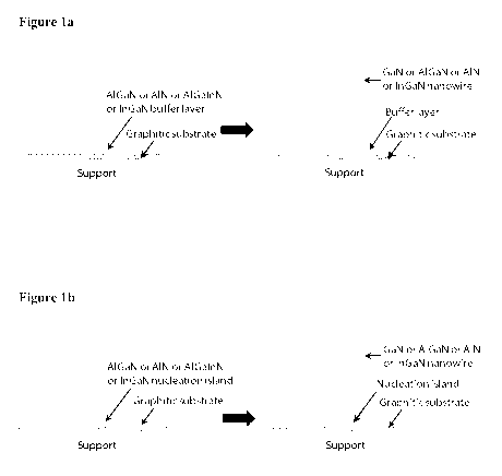
In a first embodiment, a thin buffer layer or nanoscale nucleation islands
could be grown on the graphitic surface. The buffer layer could be made of AIN
or
AlGaN or AlGaInN or InGaN, which enhances the density, and controls the
polarity
and orientation of nanowires or nanopyramids such as GaN. Use of AIN buffer
layer
has been previously reported for GaN nanowire or nanopyramid growth on Si
substrates (Nanotechno logy 26 (2015) 085605); however, not on graphitic
substrates. The buffer layer on the graphitic substrate can be grown by
migration
enhanced epitaxy (MEE). Tuning the growth conditions, such as temperature and
V/III ratio, and the thickness of the buffer layer, the density, alignment and
polarity
of the nanowires or nanopyramids can be controlled.
In an alternative process, the inventors observed that instead of using a
buffer layer, nanoscale nucleation islands of AIN or AlGaN or AlGaInN or InGaN
on graphitic substrate can be used to facilitate the growth of nanowires or
nanopyramids. These nucleation islands increase the density, and control the
polarity
and alignment of nanowires or nanopyramids. More specifically, AlGaN islands
can
be grown on a graphitic substrate. The density of the islands can be increased
by
increasing the island growth time. Then the nanowire or nanopyramid growth
(e.g.
GaN or AlGaN) can be initiated on the said islands.
The use of nucleation islands as compared to a buffer layer has some
additional advantages. For example the graphitic surface does not get covered
by the
buffer layer that might reduce the transparency of graphene. Furthermore,
since the
nucleation island size (typically 5-20 nm) is much smaller than the nanowire
or
nanopyramid diameter (typically 50-500 nm), the electrical conduction path
between
nanowire or nanopyramid and graphene is not much compromised; especially, with
CA 02993884 2018-01-26
WO 2017/021380 PCT/EP2016/068350
- 10 -
regard to the case when the buffer layer is undoped or has a higher bandgap
(e.g.
AN and AlGaN) than the nanowire or nanopyramid (e.g. GaN and InGaN).
In a further embodiment, before nanowire or nanopyramid growth the
graphitic surface is subjected to a nitrogen plasma, leading to the
incorporation of
nitrogen as a substitutional impurity or/and formation of ledges and step
edges on its
surface, preferably both. The atomic ledges facilitate the nucleation of
nanowires or
nanopyramids as mentioned above. The inclusion of nitrogen changes the Fermi
level and hence the electronic structure of the graphitic substrate (Nano
Lett. 8,
4373, (2008)). The inclusion of nitrogen also increases the chemical
reactivity of
the graphitic substrate and makes nanowire or nanopyramid nucleation on the
surface easier. In particular, doping, such as n-type doping of the graphene
in
combination with nitrogen plasma may facilitate nanowire or nanopyramid growth
and further device fabrication.
In an alternative process, the invention relates to the introduction of a
buffer
layer or nanoscale islands of an Al¨group V compound such as AlAs, AlAsSb or
AlSb on the graphitic substrate.
Al is first deposited on the graphitic substrate to form a thin Al layer or
nanoscale Al islands on the graphitic substrate. Due to the relatively high
binding
energy and thus a low diffusion coefficient of the Al adatoms, Al tends to
stick on
the graphitic surface. Group V element flux such as As and/or Sb fluxes are
provided onto the above Al layer or nanoscale islands, thereby forming a
buffer
layer or nanoscale islands of Al-group V compound such as AlAs, AlAsSb or
AlSb.
A change in the surface energy by the introduction of the buffer layer or
nanoscale
islands facilitates the nucleation and growth of nanowires or nanopyramids.
The
flux may be in the form of monomers, dimers, trimers or tetramers, such as As2
and
Sb2.
In particular, an Al layer of nominal thickness 0.01 to 2 nm is deposited on
the graphitic substrate such as at temperatures between 500-700 C. The layer
is
then transformed into a buffer layer or nanoscale islands of AlAs, AlAsSb or
AlSb
by supplying As and/or Sb fluxes such as in the range of 0.05-5x10⁻⁶ Torr,
such as
1-3x10⁻⁶ Torr. Then Ga droplets are formed on the said buffer layer or
nanoscale
islands by supplying only Ga flux to catalyse the growth of a plurality of
CA 02993884 2018-01-26
WO 2017/021380 PCT/EP2016/068350
- 11 -
semiconducting group III-V nanowires, preferably nanowires comprising GaAs
and/or GaAsSb, on said buffer layer or nucleation islands on the graphitic
substrate,
preferably via MOVPE or MBE. Nanowires preferably grow perpendicular to the
substrate.
In a further embodiment, defects and holes of single or multiple atomic
layers in depth are formed on the graphitic substrate. We also call these
defects or
holes steps or ledges. In other words therefore, many steps are created on the
graphitic substrate that aid the nucleation of nanowires or nanopyramids. This
can
be achieved through treatment with oxygen plasma or through treatment with
ozone,
e.g. UV and ozone. The treatment is preferably effected at elevated
temperature,
such as 100 C or more, ideally 125 to 175 C, such as 150 C. The etching
process
appears to work better at these slightly elevated temperatures. Moreover, the
use of
elevated temperatures begins the annealing process described below.
As well as introducing steps or ledges or alternatively to the introduction of
steps or ledges, this treatment introduces oxygen atoms to the surface of the
graphitic layer, typically via the formation of an epoxide group on the
graphitic
surface. Preferably, the treatment introduces both ledges/steps and oxygen
atoms to
the surface of the graphitic layer. The use of elevated temperatures during
the
treatment process may also enhance the etching process (i.e. the formation of
ledges).
Preferably, this surface treatment results in the formation of a rough
graphitic
surface, with holes and defects on the surface of the graphitic substrate, and
the
carbon dangling bonds are bonded with oxygen atoms. The introduction of ledges
onto the substrate surface increases the surface roughness and creates a
fluctuation
in surface potential of the substrate making nucleation thereon easier.
The surface of the UV-ozone or oxygen plasma treated graphitic substrate
could itself be used as a surface for nanowire or nanopyramid nucleation;
however,
the inventors have found that annealing the treated graphitic substrate with
hydrogen
results in a more interesting surface for nanowire or nanopyramid nucleation.
In particular, therefore the ozone or oxygen plasma treated graphitic
substrate is annealed in the presence of hydrogen, typically in an inert
atmosphere.
The annealing process may take place at a temperature of 100 to 500 'C, such
as 250
CA 02993884 2018-01-26
WO 2017/021380 PCT/EP2016/068350
- 12 -
to 400 C. A suitable graphene treatment process is described in Science 330
(2010)
655. The inert gas is typically nitrogen or a noble gas such as argon. The
annealing
process reduces the epoxide surface groups at the ledges down to C-H groups
and
therefore provides an improved surface for nanowire or nanopyramid nucleation
and
hence nanowire or nanopyramid growth. Without wishing to be limited by theory,
the C-H bond is believed to break at the elevated temperatures used for
nanowire or
nanopyramid growth, leaving the surface with dangling bond for the nanowire or
nanopyramid nucleation to take place. Also, it is believed that the oxygen or
ozone
treatment causes vertical etching of the graphitic substrate and hence the
introduction of ledges/steps. The annealing process causes lateral etching
increasing
surface roughness across the surface of the substrate.
In a final embodiment, the invention relates to the introduction of a
crystalline Si layer, in particular an alpha-crystalline Si(111) layer onto
the graphitic
substrate using the metal-induced crystallization (MIC) process. This
crystalline Si
layer allows nanowire or nanopyramid growth in the [111] direction and hence
the
formation of perpendicular nanowires or nanopyramids.
It is very difficult to introduce a Si(111) layer directly onto a graphitic
substrate however. The inventors therefore propose to introduce first an Al
layer on
the substrate. That Al layer can be deposited by any known technique such as e-
beam or thermal evaporation, atomic layer deposition (ALD), CVD and so on.
Especially, the inventors have shown that the electron beam evaporation of Al
can
be used, something which ensures that the graphitic surface is not damaged in
said
process.
Ideally, the graphitic surface is modified only at those spots where nanowires
are to nucleate, whereas the rest of the graphitic surface should remain
undamaged
in order to keep the good electrical properties of the graphitic surface
between the
nanowires or nanopyramids.
The Al layer is preferably 10 to 30 nm in thickness. The uppermost atomic
layers of this Al layer are preferably oxidised by exposing the Al to an
oxygen
source such as air. The uppermost atomic layers are preferably represented by
around the top 5 nm of the Al layer.
CA 02993884 2018-01-26
WO 2017/021380 PCT/EP2016/068350
- 13 -
Thereafter, a Si layer is applied on top of the oxidised Al layer (aluminium
oxide layer). Again, the same application techniques can be employed. The Si
layer
is amorphous at this point. Thus, a structure is preferably formed in which a
graphitic substrate carries an Al layer, an oxidised Al layer and an amorphous
Si
layer, in that order. The Si layer can be 5 to 50 nm in thickness
It is then possible to heat the composition in order to interchange the
positions of the Al and Si layers. Annealing may take place at a temperature
of 300
to 500 C. Typically, annealing occurs in an inert atmosphere, such as an
atmosphere of nitrogen.
Without wishing to be limited by theory, in general the as-deposited Al layer
on arbitrary substrates is polycrystalline with no preferential orientation of
the
grains. The Si layer is also amorphous at this stage with no crystalline Si
before
annealing. Therefore, the initial bilayer consists of amorphous Si on top of
polycrystalline Al, with a thin oxide interface. On annealing, Si atoms
diffuse into
the Al layer and form spontaneously crystalline nuclei. The driving force is
the free
energy difference between the amorphous and crystalline phases of Si. At the
end of
the crystallization process, the Al and Si layers have exchanged their initial
stacking
position: the Al layer is on top of the stack. Typically, a (Si)Al-oxide layer
is
located between the Al and Si layers at this point. Depending on the
crystallinity of
the Al layer and its oxidation condition, the crystallization of Si grains is
determined.
A similar process is described in Nano Lett. 13, 2743 (2013). A similar
disclosure can also be found in J. Appl. Phys. 115, 094301 (2014). However,
these
reference papers have not carried out the process on a conducting substrate,
especially a graphitic substrate. Moreover the sputtering method was used to
deposit
the (111)-oriented Al layer for the crystallization of (111)-oriented Si film
on the
substrates. The deposition of Al by sputtering is, however, not suitable for
graphitic
substrates. High energy ions in plasma generated during the sputter process
can
easily damage the carbon bonds in graphene.
The present inventors have found that the electron beam evaporation of Al
on graphene can give a preferable (111)-orientation of the Al layer, which is
much
enhanced compared to that on amorphous 5i02 substrates. This subsequently
results
CA 02993884 2018-01-26
WO 2017/021380 PCT/EP2016/068350
- 14 -
in a highly (111)-oriented Si film on graphene after the AIC process without
any
damage in the graphene substrate.
The Al layer can then be removed, preferably via etching of the Al layer (as
well as any (Si)Al-oxide in-between the two layers) to leave a substrate
coated with
a mainly (111) crystalline nanostructured Si layer on the graphitic substrate.
The Si
layer at this point can be 5 to 50 nm in thickness. Since the Si layer is very
thin, the
properties of underlying graphene can still be realised, i.e. it will still be
flexible,
conductive and mostly transparent. A further advantage of using the Si layer
is that
the nanowire or nanopyramid growth recipe can readily be transferred from the
growth on standard Si(111) substrates. Since the nanowire or nanopyramid
growth
takes place on the Si layer on top of graphic substrate, the standard recipes
for
growing III-V nanowires or nanopyramids on Si can readily be applied.
Moreover,
the density of nanowires or nanopyramids is much higher than on the bare
graphitic
substrate. In addition one can grow nanowires or nanopyramids at a higher
temperature which is generally used for the nanowire or nanopyramid growth on
Si(111) instead of the two step growth of nanowires or nanopyramids on
graphitic
substrates involving a low-temperature step, which is the cause for the two-
dimensional growth of (unwanted) parasitic III-V semiconductor materials. This
would decrease the parasitic crystal growth of III-V semiconductor materials
on the
substrate. Combining with a mask with hole pattern on top of the Si(111)
layer, one
can achieve the nanowire or nanopyramid growth only at exposed hole region by
high temperature growth, resulting in a positon-controlled or selective area
growth.
Support for substrate
The graphitic substrate may need to be supported in order to allow growth of
the nanowires or nanopyramids thereon. The substrate can be supported on any
kind
of material including conventional semiconductor substrates and transparent
glasses.
It is preferred if the support is transparent so that the substrate does not
block light
from exiting or entering the device.
Examples of preferred substrates include fused silica, fused quartz, fused
alumina, silicon carbide or AN. The use of fused silica or SiC is preferred,
CA 02993884 2018-01-26
WO 2017/021380 PCT/EP2016/068350
- 15 -
especially fused silica. The support should be inert. After nanowire or
nanopyramid growth and before use in a device, the support might be removed,
e.g.
by peeling away the support from the graphitic substrate.
Growth of Nanowires or Nanopyramids
In order to prepare nanowires or nanopyramids of commercial importance, it
is preferred that these grow epitaxially on the substrate, Si layer, buffer
layer or
nucleation islands. It is also ideal if growth occurs perpendicular to the
growing
surface and ideally therefore in the [111] (for cubic crystal structure) or
[0001] (for
hexagonal crystal structure) direction.
The present inventors have determined that epitaxial growth on graphitic
substrates is possible by determining a possible lattice match between the
atoms in
the semiconductor nanowire or nanopyramid and the carbon atoms in the graphene
sheet.
The carbon-carbon bond length in graphene layers is about 0.142 nm.
Graphite has hexagonal crystal geometry. The present inventors have previously
realised that graphite can provide a substrate on which semiconductor
nanowires or
nanopyramids can be grown as the lattice mismatch between the growing nanowire
or nanopyramid material and the graphitic substrate can be very low.
The inventors have realised that due to the hexagonal symmetry of the
graphitic substrate and the hexagonal symmetry of the semiconductor atoms in
the
(111) planes of a nanowire or nanopyramid growing in the [111] direction with
a
cubic crystal structure (or in the (0001) planes of a nanowire or nanopyramid
growing in the [0001] direction with a hexagonal crystal structure), a lattice
match
can be achieved between the growing nanowires or nanopyramids and the
substrate.
A comprehensive explanation of the science here can be found in
W02013/104723.
Without wishing to be limited by theory, due to the hexagonal symmetry of
the carbon atoms in graphitic layers, and the hexagonal symmetry of the atoms
of
cubic or hexagonal semiconductors in planes normal to the [111] and [0001]
crystal
direction, respectively, (a preferred direction for most nanowire or
nanopyramid
CA 02993884 2018-01-26
WO 2017/021380 PCT/EP2016/068350
- 16 -
growth), a close lattice match between the graphitic substrate and
semiconductor can
be achieved when the semiconductor atoms are placed above the carbon atoms of
the graphitic substrate, ideally in a hexagonal pattern. This is a new and
surprising
finding and can enable the epitaxial growth of nanowires or nanopyramids on
graphitic substrates.
The different hexagonal arrangements of the semiconductor atoms as
described in W02013/104723, can enable semiconductor nanowires or
nanopyramids of such materials to be vertically grown to form free standing
nanowires or nanopyramids on top of a thin carbon-based graphitic material.
In a growing nanopyramid, the triangular faces are normally terminated with
(1-101) or (1-102) planes. The triangular side surfaces with (1-101) facets
could
either converge to a single point at the tip or could form a new facets ((1-
102)
planes) before converging at the tip. In some cases, the nanopyramids are
truncated
with its top terminated with {0001} planes.
Whilst it is ideal that there is no lattice mismatch between a growing
nanowire or nanopyramid and the substrate, nanowires or nanopyramids can
accommodate much more lattice mismatch than thin films for example. The
nanowires or nanopyramids of the invention may have a lattice mismatch of up
to
about 10% with the substrate and epitaxial growth is still possible. Ideally,
lattice
mismatches should be 7.5% or less, e.g. 5% or less.
For some semiconductors like cubic InAs (a = 6.058 A), cubic GaSb (a =
6.093 A), the lattice mismatch is so small (<1%) that excellent growth of
these
semiconductors can be expected.
The nanowire or nanopyramid grown in the present invention may be from
250 nm to several microns in length, e.g. up to 5 microns. Preferably the
nanowires
or nanopyramids are at least 1 micron in length. Where a plurality of
nanowires or
nanopyramids are grown, it is preferred if they all meet these dimension
requirements. Ideally, at least 90% of the nanowires grown will be at least 1
micron
in length. Preferably substantially all the nanowires will be at least 1
micron in
length.
Growth of nanowires/nanopyramids can be controlled through flux ratios.
Nanopyramids are encouraged, for example if high group V flux is employed.
CA 02993884 2018-01-26
WO 2017/021380 PCT/EP2016/068350
- 17 -
Moreover, it will be preferred if the nanowires grown have the same
dimensions, e.g. to within 10% of each other. Thus, at least 90% (preferably
substantially all) of the nanowires will preferably be of the same diameter
and/or the
same length (i.e. to within 10% of the diameter/length of each other).
Essentially,
therefore the skilled man is looking for homogeneity and nanowires then are
substantially the same in terms of dimensions.
The length of the nanowires or nanopyramids is often controlled by the
length of time for which the growing process runs. A longer process typically
leads
to a (much) longer nanowire.
The nanowires or nanopyramids have typically a hexagonal cross sectional
shape. The nanowire or nanopyramid may have a cross sectional diameter of 25
to
200 nm (i.e. its thickness). As noted above, the diameter is ideally constant
throughout the majority of the nanowire. Nanowire diameter can be controlled
by
the manipulation of the ratio of the atoms used to make the nanowire as
described
further below.
Moreover, the length and diameter of the nanowires or nanopyramids can be
affected by the temperature at which they are formed. Higher temperatures
encourage high aspect ratios (i.e. longer and/or thinner nanowires). The
skilled man
is able to manipulate the growing process to design nanowires of desired
dimensions.
The nanowires or nanopyramids of the invention are formed from at least
one III-V compound. Group III options are B, Al, Ga, In, and Tl. Preferred
options
here are Ga, Al and In.
Group V options are N, P, As, Sb. All are preferred.
It is of course possible to use more than one element from group (III) and/or
more than one element from group (V). Preferred compounds for nanowire or
nanopyramid manufacture include AlAs, GaSb, GaP, GaN, AN, AlGaN, AlGaInN,
GaAs, InP, InN, InGaAs, InSb, InAs, or AlGaAs. Compounds based on Al, Ga and
In in combination with N are one option. The use of GaN, AlGaN, AlInGaN or AN
is highly preferred, especially in combination with a group III-N buffer layer
or
nucleation islands.
CA 02993884 2018-01-26
WO 2017/021380
PCT/EP2016/068350
- 18 -
In some embodiments there are two group III cations with a group V anion
are preferred, such as AlGaN. The ternary compounds may therefore be of
formula
XYZ wherein X is a group III element, Y is a group III different from X, and Z
is a
group V element. The X to Y molar ratio in XYZ is preferably 0.1 to 0.9, i.e.
the
formula is preferably XxYl_xZ where subscript x is 0.1 to 0.9.
Quaternary systems might also be used and may be represented by the
formula AxBi_xCyDi_y where A and B are group III elements and C and D are
group
V elements. Again subscripts x and y are typically 0.1 to 0.9. Other options
will be
clear to the skilled man.
The nanowires or nanopyramids of the invention should preferably grow in
the [111] direction for nanowires or nanopyramids with cubic crystal structure
and
[0001] direction for nanowires or nanopyramids with hexagonal crystal
structure. If
the crystal structure of the growing nanowire or nanopyramid is cubic, then
the
(111) interface between the nanowire or nanopyramid and the catalyst droplet
represents the plane from which axial growth takes place. If the nanowire or
nanopyramid has a hexagonal crystal structure, then the (0001) interface
between the
nanowire or nanopyramid and the catalyst droplet represents the plane from
which
axial growth takes place. Planes (111) and (0001) both represent the same
(hexagonal) plane of the nanowire, it is just that the nomenclature of the
plane varies
depending on the crystal structure of the growing nanowire.
The nanowires or nanopyramids are preferably grown by MBE or MOVPE.
In the MBE method, the growing surface is provided with a molecular beam of
each
reactant, e.g. a group III element and a group V element preferably supplied
simultaneously. A higher degree of control of the nucleation and growth of the
nanowires or nanopyramids on the graphitic substrate might be achieved with
the
MBE technique by using migration-enhanced epitaxy (MEE) or atomic-layer MBE
(ALMBE) where e.g. the group III and V elements can be supplied alternatively.
A preferred technique is solid-source MBE, in which very pure elements
such as gallium and arsenic are heated in separate effusion cells, until they
begin to
slowly evaporate (e.g. gallium) or sublimate (e.g. arsenic). However, a rf-
plasma
nitrogen source is typically used to produce low energy beams of nitrogen
atoms.
The gaseous elements then condense on the substrate, where they may react with
CA 02993884 2018-01-26
WO 2017/021380 PCT/EP2016/068350
- 19 -
each other. In the example of gallium and arsenic, single-crystal GaAs is
formed.
The use of the term "beam" implies that evaporated atoms (e.g. gallium) or
molecules (e.g. As4 or As2) do not interact with each other or vacuum chamber
gases
until they reach the substrate.
MBE takes place in ultra-high vacuum, with a background pressure of
typically around 10-10 to 10-9 Torr. Nanostructures are typically grown
slowly, such
as at a speed of up to a few, such as about 10, pm per hour. This allows
nanowires
or nanopyramids to grow epitaxially and maximises structural performance.
In the MOVPE method, the substrate is kept in a reactor in which the
substrate is provided with a carrier gas and a metal organic gas of each
reactant, e.g.
a metal organic precursor containing a group III element and a metal organic
precursor containing a group V element. The typical carrier gases are
hydrogen,
nitrogen, or a mixture of the two. A higher degree of control of the
nucleation and
growth of the nanowires or nanopyramids on the graphitic substrate might be
achieved with the MOVPE technique by using pulsed layer growth technique,
where
e.g. the group III and V elements can be supplied alternatively.
The nanowires or nanopyramids of the invention may be grown with or
without the presence of a catalyst. Catalyst can be introduced to provide
nucleating
sites for nanowire or nanopyramid growth. The catalyst can be one of the
elements
making up the nanowire or nanopyramid - so called self-catalysed, or different
from
any of the elements making up the nanowire.
For catalyst-assisted growth the catalyst may be Au or Ag or the catalyst
may be a metal from the group used in the nanowire or nanopyramid growth (e.g.
group III metal), especially one of the metal elements making up the actual
nanowire
or nanopyramid (self-catalysis). It is thus possible to use another element
from
group III as a catalyst for growing a III-V nanowire, e.g. use Ga as a
catalyst for an
In-V) nanowire or nanopyramid and so on. Preferably the catalyst is Au or the
growth is self-catalysed (i.e. Ga for a Ga- V) nanowire or nanopyramid and so
on).
The catalyst can be deposited onto the growing surface to act as a nucleation
site for
the growth of the nanowires or nanopyramids. Ideally, this can be achieved by
providing a thin film of catalytic material formed over the growing surface.
When
the catalyst film is melted as the temperature increases to the nanowire or
CA 02993884 2018-01-26
WO 2017/021380 PCT/EP2016/068350
- 20 -
nanopyramid growth temperature, the catalyst forms nanometre sized particle-
like
droplets on the growing surface and these droplets form the points where
nanowires
or nanopyramids can grow.
This is called vapour-liquid-solid growth (VLS) as the catalyst is the liquid,
the molecular beam is the vapour and the nanowire or nanopyramid provides the
solid component. In some cases the catalyst particle can also be solid during
the
nanowire or nanopyramid growth, by a so called vapour-solid-solid growth (VSS)
mechanism. As the nanowire or nanopyramid grows (by the VLS method), the
liquid
(e.g. gold) droplet stays on the top of the nanowire. It remains at the top of
the
nanowire or nanopyramid after growth and may therefore play a major role in
contacting a top electrode.
In order to prepare a more regular array of self-catalysed VLS grown
nanowires or nanopyramids with better homogeneity in height and diameter of
grown nanowires or nanopyramids, a mask can be used on the substrate. This
mask
can be provided with regular holes, where catalyst particles (of one of the
group-III
elements) are deposited in the holes such that nanowires or nanopyramids can
grow
homogeneously in size in a regular array across the substrate. The hole
patterns in
the mask can be easily fabricated using conventional photo/e-beam lithography
or
nanoimprinting. Focussed ion beam technology may also be used in order to
create a
regular array of nucleation sites on the graphitic surface for the nanowire or
nanopyramid growth.
Ideally, there exists only one catalyst particle in a hole.
In order to prepare positioned Au catalysed nanowires or nanopyramids on a
substrate, a thin film of Au, such as with a thickness less than 50 nm, can be
deposited on a hole-patterned photo or e-beam resist. By removing the photo or
e-
beam resist in a so called "lift-off' process, a regular arrayed pattern of Au
dots on
the substrate surface can be fabricated.
The growth of nanowires or nanopyramids without the presence of a catalyst
is also possible and is known as selective area growth method. This method may
require a mask with nano-hole patterns deposited on the graphitic layers as
described
herein. The mask material can be an oxide or nitride masking layer, preferably
a
metal oxide or metal nitride layer or semimetal oxide or semimetal nitride).
The
CA 02993884 2018-01-26
WO 2017/021380 PCT/EP2016/068350
- 21 -
mask layer can be applied through atomic layer deposition or the techniques
discussed above in connection with the deposition of the other layers. The
oxide
used is preferably based on a metal or semimetal (such as Si). The nature of
the
cation used in the masking layer may be Al, Si or a transition metal,
especially a first
3d row transition metal (Sc-Zn). Preferred masking layers are based on oxides,
such
as 5i02, Si3N4, T102 Or A12035 W2035 and SO on.
Masking layers may be 5 to 100 nm in thickness, such as 10 to 50 nm.
The masking layer is preferably continuous and covers the substrate as a
whole. This ensures that the layer is defect-free and thus prevents nucleation
of
nanowires or nanopyramids on the masking layer.
Thus a mask can be applied to the substrate and etched with holes exposing
the substrate surface, optionally in a regular pattern. Moreover, the size and
the
pitch of the holes can be carefully controlled. By arranging the holes
regularly, a
regular pattern of nanowires or nanopyramids can be grown.
Moreover, the size of the holes can be controlled to ensure that only one
nanowire or nanopyramid can grow in each hole. Finally, the holes can be made
of
a size where the hole is sufficiently large to allow nanowire or nanopyramid
growth.
In this way, a regular array of nanowires can be grown.
The graphitic surfaces may be treated with the above mentioned techniques
(oxygen or ozone treatment and hydrogenation, nitrogen plasma, MIC of
amorphous
silicon, deposition of buffer layer, or formation of nucleation islands)
before or after
the deposition of mask.
As noted above, it is also possible to prepare self-catalysed nanowires. By
self-catalysed is meant that one of the components of the nanowire or
nanopyramid
acts as a catalyst for its growth.
For example, a Ga layer can be applied to the hole-patterned mask layer,
melted to form droplets acting as nucleation sites for the growth of Ga
containing
nanowires. Again, a Ga metal portion may end up positioned on the top of the
nanowire.
In more detail, for MBE for example, a Ga/In flux can be supplied to the
substrate surface for a period of time to initiate the formation of Ga/In
droplets on
the surface upon heating of the substrate. The substrate temperature can then
be set
CA 02993884 2018-01-26
WO 2017/021380 PCT/EP2016/068350
- 22 -
to a temperature suitable for the growth of the nanowire or nanopyramid in
question.
The growth temperature may be in the range 300 to 700 C. The temperature
employed is, however, specific to the nature of the material in the nanowire,
the
catalyst material and the substrate material. For GaAs and/or GaAsSb, a
preferred
temperature is 540 to 630 C, e.g. 590 to 630 C, such as 610 C. For InAs the
range
is lower, for example 420 to 540 C, such as 430 to 540 C, e.g. 450 C.
Nanowire or nanopyramid growth can be initiated by opening the shutter of
the Ga/In effusion cell and the counter ion effusion cell, simultaneously once
a
catalyst film has been deposited and melted.
The temperature of the effusion cells can be used to control growth rate.
Convenient growth rates, as measured during conventional planar (layer by
layer)
growth, are 0.05 to 2 gm per hour, e.g. 0.1 gm per hour.
The pressure of the molecular beams can also be adjusted depending on the
nature of the nanowire or nanopyramid being grown. Suitable levels for beam
equivalent pressures are between 1 x 10⁻⁷ and 1 x 10⁻⁵ Torr.
The beam flux ratio between reactants (e.g. group III atoms and group V
molecules) can be varied, the preferred flux ratio being dependent on other
growth
parameters and on the nature of the nanowire or nanopyramid being grown.
It has been found that the beam flux ratio between reactants can affect
crystal
structure of the nanowire. For example, using Au as a catalyst, growth of GaAs
nanowires with a growth temperature of 540 C, a Ga flux equivalent to a
planar
(layer by layer) growth rate of 0.6 [tm per hour, and a beam equivalent
pressure
(BEP) of 9 x 10⁻⁶ Ton for As4 produces wurtzite crystal structure. As opposed
to
this, growth of GaAs nanowires at the same growth temperature, but with a Ga
flux
equivalent to a planar growth rate of 0.9 [tm per hour and a BEP of 4 x 10⁻⁶
Ton for
As4, produces zinc blende crystal structure.
Nanowire or nanopyramid diameter can in some cases be varied by changing
the growth parameters. For example, when growing self-catalyzed GaAs nanowires
under conditions where the axial nanowire or nanopyramid growth rate is
determined by the As4 flux, the nanowire or nanopyramid diameter can be
increased/decreased by increasing/decreasing the Ga:As4 flux ratio. The
skilled
CA 02993884 2018-01-26
WO 2017/021380 PCT/EP2016/068350
- 23 -
man is therefore able to manipulate the nanowire or nanopyramid in a number of
ways.
It is thus an embodiment of the invention to employ a multistep, such as two
step, growth procedure, e.g. to separately optimize the nanowire or
nanopyramid
nucleation and nanowire or nanopyramid growth.
A significant benefit of MBE is that the growing nanowire or nanopyramid
can be analysed in situ, for instance by using reflection high-energy electron
diffraction (RHEED). RHEED is a technique typically used to characterize the
surface of crystalline materials. This technology cannot be applied so readily
where
nanowires are formed by other techniques such as MOVPE.
The nanowires of the invention preferably grow as cubic (zinc blende) or
hexagonal (wurtzite) structures. The inventors have found that it is possible
to
change the crystal structure of the growing nanowire or nanopyramid by
manipulating the amounts of the reactants fed to the substrate as discussed
above.
Higher feeds of Ga, for example, force a GaAs crystal into the cubic crystal
structure. Lower feeds encourage a hexagonal structure. By manipulating
reactant
concentrations, the crystal structure within the nanowire or nanopyramid can
therefore be changed.
A significant benefit of MOVPE is that the nanowires or nanopyramids can
be grown at a much faster growth rate. Both radial and axial heterostructured
nanowires can be grown using the MOVPE method. However, for certain III-V
semiconductors such as III-nitrides, this method favours the growth of radial
heterostructured nanowires and microwires, for example: n-doped GaN core with
shell consisting of intrinsic GaN/InGaN multiple quantum wells (MQW), p-doped
AlGaN electron blocking layer (EBL) and p-doped GaN shell. This method also
allows the growth of axial heterostructured nanowires using techniques such as
pulsed growth technique or continuous growth mode with modified growth
parameters for e.g., lower V/III molar ratio and higher substrate temperature.
In more detail, the reactor is evacuated after placing the sample, and is
purged with N2 to remove oxygen and water in the reactor. This is to avoid any
damage to the graphitic substrate at the growth temperatures, and to avoid
unwanted
reactions of oxygen and water with the precursors. The reactor pressure is set
to be
CA 02993884 2018-01-26
WO 2017/021380 PCT/EP2016/068350
- 24 -
between 50 and 400 Torr. After purging the reactor with N2, the substrate is
thermally cleaned under H2 atmosphere at a substrate temperature of about 1200
C.
Subsequently, a very thin buffer layer or nucleation islands is grown which
consists
of Al(In)GaN or AN by introducing metal organic precursors and NH3. The metal
organic precursors can be either trimethylgallium (TMGa), or triethylgallium
(TEGa) for Ga, trimethylalumnium (TMA1) or triethylalumnium (TEA1) for Al, and
trimethylindium (TMIn) or triethylindium (TEIn) for In. The metal precursors
for
dopants can be SiH4 for silicon and bis(cyclopentadienyl)magnesium (Cp2Mg) or
bis(methylcyclopentadienyl)magnesium ((MeCp)2Mg) for Mg. During the
Al(In)GaN or AN buffer layer or nucleation islands deposition, the substrate
temperature may be set in the range of 600 to 1200 C. The flow rates of TMGa,
TMA1 and TMIn can be maintained between 5 and 100 sccm. The NH3 flow rate can
be varied between 5 and 550 sccm. TMGa/TMA1 and NH3 are supplied to the
substrate surface for a period of time to initiate the formation of Al(In)GaN
or AN
buffer layer or nucleation islands on the graphitic surface. The growth
parameters
used for buffer layer or nucleation islands can strongly influence the
density,
polarity and alignment of the nanowires. The substrate temperature can then be
set
to a temperature suitable for the growth of the nanowire or nanopyramid in
question.
The growth temperature may be in the range 700 to 1200 C. The temperature
employed is, however, specific to the nature of the material in the nanowire.
For
GaN nanowires, a preferred temperature is 800 to 1150 C, e.g. 900 to 1100 C,
such
as 1100 C. For AlGaN nanowires or nanopyramids, the range is slightly higher,
for
example 900 to 1400 C, such as 1050 to 1250 C, e.g. 1250 C.
The nanowires or nanopyramids of the invention preferably grow epitaxially.
They attach to the underlying substrate through covalent, ionic or quasi van
der
Waals binding. Accordingly, at the junction of the growing surface and the
base of
the nanowire, crystal planes are formed epitaxially within the nanowire. These
build
up, one upon another, in the same crystallographic direction thus allowing the
epitaxial growth of the nanowire. Preferably the nanowires or nanopyramids
grow
perpendicularly. It will be appreciated that in experimental science the
growth angle
may not be exactly 90 but the term perpendicularly implies that the nanowires
are
within about 10 of perpendicular, e.g. within 5 . Because of the epitaxial
growth
CA 02993884 2018-01-26
WO 2017/021380 PCT/EP2016/068350
- 25 -
via covalent, ionic or quasi van der Waals bonding, it is expected that there
will be
an intimate contact between the nanowires or nanopyramids and the growing
surface. To enhance the contact property further, the substrate can be doped
to
match the major carriers of grown nanowires or nanopyramids.
Because nanowires or nanopyramids are epitaxially grown involving
physical and chemical bonding to growing surfaces at high temperature, the
bottom
contact is preferably ohmic.
It will be appreciated that the inventive compositions comprise a plurality of
nanowires or nanopyramids. Preferably the nanowires or nanopyramids grow about
parallel to each other. It is preferred therefore if at least 90%, e.g. at
least 95%,
preferably substantially all nanowires or nanopyramids grow in the same
direction
from the same plane of the growing surface.
It will be appreciated that there are many planes from which epitaxial growth
could occur. It is preferred if substantially all nanowires or nanopyramids
grow
from the same plane. It is preferred if that plane is parallel to the
substrate surface.
Ideally the grown nanowires or nanopyramids are substantially parallel.
Preferably,
the nanowires or nanopyramids grow substantially perpendicular to the growing
surface.
Doping
The nanowires or nanopyramids of the invention can contain a p-n or p-i-n
junction, e.g. to enable their use in LEDs. Nanowires or nanopyramids of the
invention are therefore provided with an undoped intrinsic semiconductor
region
between a p-type semiconductor and an n-type semiconductor region. All of or
sections of the p-type and n-type regions are typically heavily doped because
they
are used for ohmic contacts.
It is therefore preferred that the nanowires or nanopyramids are doped.
Doping typically involves the introduction of impurity ions into the nanowire,
e.g.
during MBE or MOVPE growth. The doping level can be controlled from
¨1015/cm3to 1020/cm3. The nanowires or nanopyramids can be p-doped or n-doped
as desired. Doped semiconductors are extrinsic semiconductors.
CA 02993884 2018-01-26
WO 2017/021380 PCT/EP2016/068350
- 26 -
The 11(p)-type semiconductors have a larger electron (hole) concentration
than hole (electron) concentration by doping an intrinsic semiconductor with
donor
(acceptor) impurities. Suitable donor (acceptors) for III-V compounds can be
Te
(Mg, Be and Zn). Dopants can be introduced during the growth process or by ion
implantation of the nanowires or nanopyramids after their formation.
Higher carrier injection efficiency is required to obtain higher external
quantum efficiency (EQE) of LEDs. However, the increasing ionization energy of
Mg acceptors with increasing Al content in AlGaN alloys makes it difficult to
obtain
higher hole concentration in AlGaN alloys with higher Al content. To obtain
higher
hole injection efficiency (especially in the p-region layers consisting of
high Al
content), the inventors have devised a number of strategies which can be used
individually or together.
There are problems to overcome in the doping process therefore. It is
preferred if the nanowires or nanopyramids of the invention comprise Al. The
use
of Al is advantageous as high Al content leads to high band gaps, enabling UV-
C
LED emission from the active layer(s) of nanowires or nanopyramids and/or
avoiding absorption of the emitted light in the p-region and/or n-region
layers.
Where the band gap is high, it is less likely that UV light is absorbed by
this part of
the nanowires or nanopyramids. The use therefore of AIN or AlGaN in nanowires
or nanopyramids is preferred.
However, p-type doping of AlGaN or AN to achieve high electrical
conductivity (high hole concentration) is challenging as the ionization energy
of Mg
or Be acceptors increases with increasing Al content in AlGaN alloys. The
present
inventors propose various solutions to maximise electrical conductivity (i.e.
maximise hole concentration) in AlGaN alloys with higher average Al content.
Where the nanowires or nanopyramids comprise AN or AlGaN, achieving
high electrical conductivity by introducing p-type dopants is a challenge.
One solution relies on a short period superlattice (SPSL). In this method, we
grow a
superlattice structure consisting of alternating layers with different Al
content
instead of a homogeneous AlGaN layer with higher Al composition. For example,
a
p-region layer with 35% Al content could be replaced with a 1.8 to 2.0 nm
period
SPSL consisting of, for example, alternating AlxGai_xN:Mg / AlyGai_yN:Mg with
CA 02993884 2018-01-26
WO 2017/021380 PCT/EP2016/068350
- 27 -
x=0.30/y=0.40. The low ionization energy of acceptors in layers with lower Al
composition leads to improved hole injection efficiency without compromising
on
the barrier height in the p-region layer. This effect is additionally enhanced
by the
polarization fields at the interfaces. The SPSL can be followed with a highly
p-
doped GaN:Mg layer for better hole injection.
More generally, the inventors propose to introduce a p-type doped Al,Gal_
,N/AlyGal_yN short period superlattice (i.e. alternating thin layers of
AlõGal,N and
AlyGal_yN) into the nanowires or nanopyramid structure, where the Al mole
fraction
x is less than y, instead of a p-type doped ALGal,N alloy where x <z <y. It is
appreciated that x could be as low as 0 (i.e. GaN) and y could be as high as 1
(i.e.
AN). The superlattice period should preferably be 5 nm or less, such as 2 nm,
in
which case the superlattice will act as a single ALGal,N alloy (with z being a
layer
thickness weighted average of x and y) but with a higher electrical
conductivity than
that of the ALGal,N alloy, due to the higher p-type doping efficiency for the
lower
Al content Al,Gai,N layers.
In the nanowires or nanopyramids comprising a p-type doped superlattice, it
is preferred if the p-type dopant is an alkali earth metal such as Mg or Be.
A further option to solve the problem of doping an Al containing
nanowire/nanopyramid follows similar principles. Instead of a superlattice
containing thin AlGaN layers with low or no Al content, a nanostructure can be
designed containing a gradient of Al content (mole fraction) in the growth
direction
of the AlGaN within the nanowires or nanopyramids. Thus, as the nanowires or
nanopyramids grow, the Al content is reduced/increased and then
increased/reduced
again to create an Al content gradient within the nanowires or nanopyramids.
This may be called polarization doping. In one method, the layers are graded
either from GaN to AN or AN to GaN. The graded region from GaN to AN and
AN to GaN may lead to n-type and p-type conduction, respectively. This can
happen due to the presence of dipoles with different magnitude compared to its
neighbouring dipoles. The GaN to AN and AN to GaN graded regions can be
additionally doped with n-type dopant and p-type dopant respectively.
In a preferred embodiment, p-type doping is used in AlGaN nanowires using
Be as a dopant.
CA 02993884 2018-01-26
WO 2017/021380 PCT/EP2016/068350
- 28 -
Thus, one option would be to start with a GaN nanowire/nanopyramid and
increase Al and decrease Ga content gradually to form AN, perhaps over a
growth
thickness of 100 nm. This graded region could act as a p- or n-type region,
depending on the crystal plane, polarity and whether the Al content is
decreasing or
increasing in the graded region, respectively. Then the opposite process is
effected
to produce GaN once more to create an n- or p-type region (opposite to that
previously prepared). These graded regions could be additionally doped with n-
type
dopants such as Si and p-type dopants such as Mg or Be to obtain n- or p-type
regions with high charge carrier density, respectively. The crystal planes and
polarity is governed by the type of nanowire/nanopyramid as is known in the
art.
Viewed from another aspect therefore, the nanowires or nanopyramids of the
invention comprise Al, Ga and N atoms wherein during the growth of the
nanowires
or nanopyramids the concentration of Al is varied to create an Al
concentration
gradient within the nanowires or nanopyramids.
In a third embodiment, the problem of doping in an Al containing nanowire
or nanopyramid is addressed using a tunnel junction. A tunnel junction is a
barrier,
such as a thin layer, between two electrically conducting materials. In the
context of
the present invention, the barrier functions as an ohmic electrical contact in
the
middle of a semiconductor device.
In one method, a thin electron blocking layer is inserted immediately after
the active region, which is followed by a p-type doped AlGaN layer with Al
content
higher than the Al content used in the active layers. The p-type doped layer
is
followed by a highly p-type doped AlGaN layer and a very thin tunnel junction
layer
followed by an n-type doped AlGaN layer. The tunnel junction layer is chosen
such
that the electrons tunnel from the valence band in p-AlGaN to the conduction
band
in the n-AlGaN, creating holes that are injected into the p-AlGaN layer.
More generally, it is preferred if the nanowire or nanopyramid comprises two
regions of doped GaN (one p- and one n-doped region) separated by an Al layer,
such as a very thin Al layer. The Al layer might be a few nm thick such as 1
to 10
nm in thickness. It is appreciated that there are other optional materials
that can
serve as a tunnel junction which includes highly doped InGaN layers.
CA 02993884 2018-01-26
WO 2017/021380 PCT/EP2016/068350
- 29 -
It is particularly surprising that doped GaN layers can be grown on the Al
layer.
In one embodiment therefore, the invention provides a nanowire or
nanopyramid having a p-type doped (A1)GaN region and an n-type doped (A1)GaN
region separated by an Al layer.
The nanowires or nanopyramids of the invention can be grown to have a
heterostructured form radially or axially. For example for an axial
heterostructured
nanowire, p-n junction can be axially formed by growing a p-type doped core
first,
and then continue with an n-doped core (or vice versa). For a radially
heterostructured nanowire, p-n junction can be radially formed by growing the
p-
doped nanowire or nanopyramid core first, and then the n-doped semiconducting
shell is grown (or vice versa) - a core shell nanowire. An intrinsic shell can
be
grown between doped regions to obtain a radially heterostructured nanowire or
nanopyramid with p-i-n junction.
It is preferred if the nanowires or nanopyramids are grown axially and are
therefore formed from a first section and a second section. The two sections
are
doped differently to generate a p-n junction or p-i-n junction. It does not
matter
whether the top or bottom section of the nanowire or nanopyramid is the p-
doped or
n-doped section.
Top contact
If the nanowires have been grown on a substrate in the presence of a catalyst,
it is envisaged that some of the nanowires will have a catalyst deposit on top
of
nanowire. Ideally, the majority of the nanowires will have such a deposit,
preferably
substantially all the nanowires will comprise this deposit.
In order to create some devices of the invention, the top of the nanowires or
nanopyramids needs to comprise a top contact.
In one preferred embodiment, a top contact is formed using another graphitic
layer. The invention then involves placing a graphitic layer on top of the
formed
nanowires or nanopyramids to make a top contact. It is preferred that the
graphitic
top contact layer is substantially parallel with the substrate layer. It will
also be
CA 02993884 2018-01-26
WO 2017/021380 PCT/EP2016/068350
- 30 -
appreciated that the area of the graphitic layer does not need to be the same
as the
area of the substrate. It may be that a number of graphitic layers are
required to
form a top contact with a substrate with an array of nanowires or
nanopyramids.
The graphitic layers used can be the same as those described in detail above
in connection with the substrate. The top contact is graphitic, more
especially it is
graphene. This graphene top contact should contain no more than 10 layers of
graphene or its derivatives, preferably no more than 5 layers (which is called
as a
few-layered graphene). Especially preferably, it is a one-atom-thick planar
sheet of
graphene.
The crystalline or "flake" form of graphite consists of many graphene sheets
stacked together (i.e. more than 10 sheets). It is preferred if the top
contact is 20 nm
in thickness or less. Even more preferably, the graphitic top contact may be 5
nm or
less in thickness.
When graphene contacts directly to the semiconductor nanowires, it usually
forms a Schottky contact which hinders the electrical current flow by creating
a
barrier at the contact junction. Due to this problem, the research on graphene
deposited on semiconductors has been mainly confined to the use of
graphene/semiconductor Schottky junctions.
However, the inventors have realized that the growing of semiconductor
nanowires can involve metal catalysis. In the VLS method, e.g. MBE or MOVPE,
the metal catalysts such as Au, Ga, or In are preferably used as seeds for
nanowire or
nanopyramid growth and they remain as a form of nanoparticles on top of
nanowires
after completion of the nanowire or nanopyramid growth. These catalyst
deposits
can be used as an intermediate material between metallic graphene and
semiconductor nanowires. By taking advantage of the remaining catalytic
material,
the Schottky contact formed at the interface between metallic graphitic top
contact
and the semiconductor nanowire or nanopyramid can be avoided and ohmic contact
can be established.
Application of the top contact to the formed nanowires can be achieved by
any convenient method. Methods akin to those mentioned previously for
transferring graphitic layers to substrate carriers may be used. The graphitic
layers
from Kish graphite, highly ordered pyrolytic graphite (HOPG), or CVD may be
CA 02993884 2018-01-26
WO 2017/021380 PCT/EP2016/068350
-31 -
exfoliated by mechanical or chemical methods. Then they can be transferred
into
etching solutions such as HF or acid solutions to remove Cu (Ni, Pt, etc.)
(especially
for CVD grown graphitic layers) and any contaminants from the exfoliation
process.
The etching solution can be further exchanged into other solutions such as
deionised
water to clean the graphitic layers. The graphitic layers can then be easily
transferred
onto the formed nanowires as the top contact. Again e-beam resist or
photoresist
may be used to support the thin graphitic layers during the exfoliation and
transfer
processes, which can be removed easily after deposition.
It is preferred if the graphitic layers are dried completely after etching and
rinsing, before they are transferred to the top of the nanowire or nanopyramid
arrays.
To enhance the contact between graphitic layers and nanowires a mild pressure
and
heat can be applied during this "dry" transfer.
Alternatively, the graphitic layers can be transferred on top of the nanowire
or nanopyramid arrays, together with a solution (e.g. deionised water). As the
solution dries off, the graphitic layers naturally form a close contact to
underlying
nanowires. In this "wet" transfer method, the surface tension of the solution
during
the drying process might bend or knock out the nanowire or nanopyramid arrays.
To
prevent this, where this wet method is used, more robust nanowires are
preferably
employed. Nanowires having a diameter of > 80 nm might be suitable.
Alternatively, hole patterned substrates which support the perpendicular
nanowire or
nanopyramid structure could be used. One may also use the critical-point
drying
technique to avoid any damage caused by surface tension during the drying
process.
Another way to prevent this is to use supporting and electrically isolating
material as
fill-in material between nanowires. The fill-in material needs to be
transparent to the
emitted or detected light.
If there is a water droplet on a nanowire or nanopyramid array and attempts
to remove it involve, for example a nitrogen blow, the water drop will become
smaller by evaporation, but the drop will always try to keep a spherical form
due to
surface tension. This could damage or disrupt the nanostructures around or
inside
the water droplet.
CA 02993884 2018-01-26
WO 2017/021380
PCT/EP2016/068350
- 32 -
Critical point drying circumvents this problem. By increasing temperature
and pressure, the phase boundary between liquid and gas can be removed and the
water can be removed easily.
The top contact graphitic layer is preferably transparent, conductive and
flexible. To enhance the electrical and mechanical contact of the graphitic
layers to
the metal particles on top of as-grown nanowires further, a post-annealing
process
may be used. After the deposition of the graphitic top contact, the sample can
be
annealed in an inert atmosphere, e.g. of argon, or vacuum. Temperatures can be
up
to 600 C. Annealing times can be up to 10 min.
Also doping of the graphitic top contact can be utilized. The major carrier of
the graphitic top contact can be controlled as either holes or electrons by
doping. It
is preferable to have the same doping type in the graphitic top contact and in
the
semiconducting nanowires, especially at the region below the metal catalytic
particles, which would give a better ohmic behaviour after the post-annealing
process. For example, for a core-shell nanowire or nanopyramid with p-doping
in
the shell, p-doping of the top graphitic layers matches the carrier type
across the
metal particles at the top of the nanowire or nanopyramid shell.
It will be appreciated therefore that both top graphitic layer and the
substrate
can be doped. In some embodiments, the substrate and/or the graphitic layer is
doped by a chemical method which involves with an adsorption of organic or
inorganic molecules such as metal chlorides (FeC13, AuC13 or GaC13), NO2,
HNO3,
aromatic molecules or chemical solutions such as ammonia.
The surface of substrate and/or the graphitic layer could also be doped by a
substitutional doping method during its growth with incorporation of dopants
such
as B, N, S, or Si.
Applications
Semiconductor nanowires or nanopyramids have wide ranging utility. They
are semiconductors so can be expected to offer applications in any field where
semiconductor technology is useful. They are primarily of use in integrated
nanoelectronics and nano-optoelectronic applications.
CA 02993884 2018-01-26
WO 2017/021380 PCT/EP2016/068350
- 33 -
An ideal device for their deployment might be a solar cell in particular. One
possible device is a nanowire or nanopyramid solar cell sandwiched between two
graphene layers as the two terminals.
Such a solar cell has the potential to be efficient, cheap and flexible at the
same time. This is a rapidly developing field and further applications on
these
valuable materials will be found in the next years. The same concept can be
used to
also fabricate other opto-electronic devices such as light-emitting diodes
(LEDs),
photodetectors, waveguides and lasers.
It will be appreciated that devices of the invention are provided with
electrodes to enable charge to be passed into the device.
The invention will now be further discussed in relation to the following non
limiting examples and figures.
Brief Description of the Figures
Figure 1(a) shows a schematic representation of deposition of buffer layer on
graphitic substrate, followed by the nanowire growth.
Figure 1(b) shows a schematic representation of deposition of nucleation
islands on graphitic substrate, followed by the nanowire growth.
Figure 2 shows representative results of the formation of nucleation island
and nanowire growth scheme. (a) SEM image of AlGaN nucleation islands grown
on graphene by MOVPE. (b) SEM image of GaN nanowires grown on the AlGaN
nucleation islands on graphene by MOVPE. Inset: SEM image of GaN growth
without AlGaN nucleation islands on graphene, where no growth of perpendicular
GaN nanowires can be seen.
Figure 3(a) is a cross-sectional high-resolution scanning transmission
electron microscope (STEM) image of a GaN nanowire grown on graphene using
AlGaN nucleation islands. Figure 3(b) is a high-angle annular dark-field STEM
image of the same nanowire in (a), showing the AlGaN nucleation island.
Figure 4a is a SEM image of (A1)GaN nanopyramids of the invention grown
in a regular array. After growing the AlGaN nucleation islands, AlGaN with 3%
Al
in gas phase was grown for 150 s. Figure 4b is a closer image of said
nanopyramids.
CA 02993884 2018-01-26
WO 2017/021380
PCT/EP2016/068350
- 34 -
Figure 5: (a) Schematic diagram showing the growth of nanowires on
graphite flake and the top and bottom contacts to the nanowires. Tilted view
SEM
image (b) and high-resolution SEM image (c) of selectively grown GaN nanowires
on multi-layer graphene flakes by MBE.
Figure 6 shows an SEM image of self-catalyzed GaAsSb nanowires grown
by MBE using AlAsSb nanoscale islands for enhanced nucleation on pristine
graphitic substrate. Inset: Magnified view of the perpendicular GaAsSb
nanowires.
Figure 7 shows atomic force microscopy (AFM) topography image after the
treatment of graphite with (a) UV-ozone and (b) UV-ozone and H2 annealing in
Ar
atmosphere.
Figure 8(a) shows the AFM height profile along the solid line in Figure 6(a)
of the graphite surface after the treatment with UV-ozone.
Figure 8(b) shows the AFM height profile along the dashed line in Figure
6(b) of the graphite surface after the UV-ozone treatment and the following H2
annealing in Ar atmosphere, showing the formation of atomic steps and ledges.
(Nanowires or nanopyramids are then grown on the treated graphitic substrate.)
Figure 9(a) shows an SEM image of GaAsSb nanowires grown on untreated
pristine graphitic surface. Figure 9(b) shows an SEM image of GaAsSb nanowires
grown on UV-ozone treated and H2 annealed graphitic surface. Improved density
of
perpendicular nanowires can be seen in (b) as compared to (a).
Figure 10 shows the main process steps of aluminium-induced crystallization
(MIC) of silicon on graphene layer 1, where amorphous silicon (a-Si) layer 3
diffuses through an aluminium metal layer 2 by thermal activation. At the
graphene-
Al interface the silicon rearranges into a polycrystalline structure (p-Si)
with [111]-
orientation. The aluminium metal layer and the oxide layer above the p-Si
structure
may be etched using HC1 and HF, respectively. (Nanowires or nanopyramids are
then grown on the MIC silicon on graphene.)
Figure 11 shows an SEM image of self-catalyzed GaAs nanowires grown by
MBE on amorphous (5i02) substrate covered with MIC silicon.
Example 1
CA 02993884 2018-01-26
WO 2017/021380
PCT/EP2016/068350
- 35 -
Experimental procedure of growing GaN nanowires on graphitic surface using
AlGaN nucleation islands:
Commercial CVD-grown graphene on Cu foil, transferred on Si(001),
Si(111), and sapphire supporting substrates, were used for this experiment.
The
growth of GaN nanowires was carried out in a horizontal flow MOVPE reactor
(Aixtron 200RF). After loading the sample, the reactor was evacuated and
purged
with N2 to remove oxygen and water in the reactor. The reactor pressure was
set to
75 Torr and H2 was used as the carrier gas for the growth. Subsequently, the
substrate was thermally cleaned under H2 atmosphere at a substrate temperature
of
¨1200 C for 5 min. After that a nitridation step was carried out using NH3
flow of
600 sccm for 10 min. Subsequently, TMGa and TMA1 was introduced for 40 s with
a flow of 44.8 and 26.3 gmol/min, respectively, to grow AlGaN nucleation
islands,
followed by a 2 min nitridation step.
For the growth of GaN nanowires, the substrate temperature was lowered to
¨1150 C and the NH3 flow was set to 25 sccm. When the temperature became
stable, Si-doped GaN nanowire growth was carried out for ¨3.5 min by
introducing
TMGa and Silane with a flow of 44.8 and 0.03 gmol/min, respectively. After the
growth, the sample was cooled down under NH3 flow of 25 sccm until the
temperature dropped below 500 C.
Example 2
Experimental procedure for nanowires growth on nitrogen plasma treated
graphitic surface:
For this experiment multi-layer graphene was mechanically exfoliated from
Kish graphite flakes and then indium-bonded to a 5i02/Si supporting substrate.
A
mask material such as A1203 and 5i02 can be optionally deposited on the
graphite
flake. A big hole of 10 gm in diameter is etched in the mask material using
photolithography such that the graphite surface is exposed in the hole.
Optionally,
several periodically spaced small holes of diameter ¨100 nm can be etched
using e-
beam lithography, such that the nanowires selectively grow on the graphitic
surface
exposed in the hole. The nitrogen plasma treatment and the nanowire growth
were
CA 02993884 2018-01-26
WO 2017/021380 PCT/EP2016/068350
- 36 -
carried out in a Veeco Gen 930 MBE system equipped with a nitrogen plasma
source, a Ga dual filament cell, and an Al double-crucible cell.
The above samples are then loaded into the MBE system for sample
outgassing and nanowire growth. The samples are annealed at a substrate
temperature of 550 C for a duration of 30 min to get rid of any oxide
residues and
any other contaminants on the substrate. The substrate temperature is then
increased
to a temperature suitable for GaN nanowire growth: i.e. typically 755 C.
The temperatures of the Ga and Al effusion cell is preset to yield nominal
planar growth rate of 0.3 and 0.2 [tm per hour, respectively. The nitrogen
plasma is
generated using a RF generator power of 450 W and nitrogen gas flow of 2.8
sccm.
After the sample temperature reaches the growth temperature, the gate valve
and the
shutter in front of the nitrogen source was opened for 1 min, such that the
nitrogen
plasma is directed on to the sample. The sample can then either be subjected
to the
nanowire growth by MBE or taken out of the MBE growth chamber for the
nanowire or nanopyramid growth by MOCVD. In the case of nanowire growth by
MBE, an Al flux was supplied for 6 seconds or longer and then an Al flux and a
nitrogen plasma was supplied for 1 minute or longer. It was followed by the
opening
of the shutter in front of the Ga and nitrogen source to supply Ga flux and
nitrogen
plasma simultaneously, to initiate the growth of intrinsic (intentionally
undoped)
GaN nanowires. Si dopant was supplied to obtain n-type GaN nanowires and
either
Be or Mg dopant was supplied to obtain p-type GaN nanowires. After the growth,
all
the shutters are closed and simultaneously the substrate temperate is ramped
down.
Example 3
Experimental procedure for the MBE growth of high-yield perpendicular
GaAsSb nanowires on graphitic surface via AlAsSb nanoscale islands for
nucleation:
Nanowires are grown in a Varian Gen II Modular MBE system equipped
with a Ga dual filament cell, an Al double-crucible cell, an As valved cracker
cell,
and an Sb valved cracker cell. The cracker cells allow to fix the proportion
of
monomers, dimers and tetramers. In this example, the major species of arsenic
and
antimony are As2 and Sb2, respectively.
CA 02993884 2018-01-26
WO 2017/021380 PCT/EP2016/068350
- 37 -
Growth of NWs is performed either on a Kish graphite flake or on a graphene
film
grown on SiC substrates by using a high-temperature sublimation technique. The
graphene film samples are purchased from external supplier. The Kish graphite
samples are cleaned by isopropanol followed by a blow dry with nitrogen, then
indium-bonded to a silicon wafer and finally cleaved to provide a fresh
graphitic
surface for growth of NWs. The graphene/SiC substrates are blow dried with
nitrogen, and then indium-bonded to a silicon wafer.
The samples are then loaded into the MBE system for sample outgassing and
nanowire growth. The samples are annealed at a substrate temperature of 550 C
for
a duration of 30 min to get rid of any oxide residues on the substrate. The
substrate
temperature is then increased to a temperature suitable for GaAs or GaAsSb
nanowire growth: i.e. 630 C.
The temperatures of the Al and Ga effusion cells are preset to yield nominal
planar
growth rates of 0.1 [tm per hour and 0.7 [tm per hour, respectively. To form
the
GaAs(Sb) nanowires, an As2 flux of 2.5x10⁻⁶ Ton is used, whereas the Sb2 flux
is
set to a value in the range 0 ¨ 1x10⁻⁶ Ton (dependent on the intended GaAsSb
composition), for example 6x10⁻⁷ Torr.
The Al flux is first supplied to the surface during a time interval of
typically 1 s or
longer, while the shutters/valves for the other sources are closed. The Al
shutter is
then closed and As and/or Sb flux are supplied to the surface for a time
interval of
typically 60 s to form AlAs(Sb) nanoscale islands on the graphitic surface.
The
group V shutters and valves are then closed and the Ga shutter opened,
typically for
5 s, to supply Ga flux to the surface to initiate the formation of Ga droplets
at the
nanoscale islands. The relevant group V shutters and valves are then opened
again to
initiate the growth of nanowires. For example, in case of GaAs nanowire
growth,
only the As shutter and valve are opened at this point, whereas in case of
GaAsSb
nanowire growth, also the Sb shutter and valve are opened. The duration of the
nanowire growth depends on the intended length of the nanowires. In case of
the
GaAsSb nanowires sample depicted in Figure 6, the nanowire growth time was 5
min. The growth is stopped by closing all the shutters/valves, and
simultaneously
ramping down the substrate to room temperature.
CA 02993884 2018-01-26
WO 2017/021380
PCT/EP2016/068350
- 38 -
Example 4
Experimental procedure for UV-ozone treatment and H2 annealing of the
graphitic surface, and MBE growth of perpendicular GaAs(Sb) nanowires:
For this experiment Kish graphite flakes were used as the graphitic
substrates. The Kish graphite samples are cleaned by isopropanol followed by a
blow dry with nitrogen, then indium-bonded to a silicon wafer and finally
cleaved to
provide a fresh graphitic surface for growth of nanowires. The substrates were
treated in UV-ozone at ¨150 C for 6 min, followed by annealing in H2 at ¨300
C
for 45 min.
Nanowires are grown in the same MBE system as described in Example 3.
The major species of arsenic and antimony are As2 and Sb2, respectively.
The samples are loaded into the MBE system and outgassed at ¨550 C for a
duration of 30 min to get rid of any oxide residues on the substrate. The
substrate
temperature is then increased to a temperature suitable for GaAs or GaAsSb
nanowire growth: i.e. 630 C.
The temperatures of the Ga effusion cell is preset to yield nominal planar
growth rate of 0.7 [tm per hour. To form Ga droplet, Ga flux was supplied for
10 s at
a substrate temperature of ¨630 C. After that the temperature is reduced to
¨250 C
and an Sb2 flux of 8x10⁻⁷ Torr and As2 flux of 2.5x10⁻⁶ Torr are subsequently
supplied for 50 s and 40 s, respectively. Then the substrate temperature is
again
increased to ¨630 C. To form the GaAs(Sb) nanowires, Ga flux was supplied for
10
min together with an As2 flux of 2.5x10⁻⁶ Torr, whereas the Sb2 flux is set to
a value
in the range 0 ¨ 1x10⁻⁶ Ton (dependent on the intended GaAsSb composition),
for
example 8x10⁻⁷ Torr. After the growth, all the shutters are closed and
simultaneously the substrate temperate is ramped down.
Example 5
Experimental procedure for the formation of Si(111) by metal induced
crystallization (MIC) on graphene
The MIC poly-Si(111) on graphene samples were of commercial chemical vapor
deposition (CVD) grown monolayer graphene transferred onto Si(001). On these
samples, 50 nm Al was deposited by e-beam evaporation at a rate of 1 A/s and a
CA 02993884 2018-01-26
WO 2017/021380 PCT/EP2016/068350
- 39 -
pressure of ¨10 8 Torr. The samples were oxidized for 24 h in an IS05
cleanroom
atmosphere before depositing 50 nm amorphous Si (a-Si) by e-beam evaporation
at a
rate of 1 A/s and a pressure of ¨10 8 Torr. All depositions were done at room
temperature. The samples were annealed for 15 h at 500 C in a nitrogen gas.
After
the layer exchange by annealing, the top layer of Al was removed by etching in
a
phosphoric acid mixture.