Note: Descriptions are shown in the official language in which they were submitted.
CA 02994503 2018-02-01
WO 2017/028948 PCT/EP2016/001387
Fabrication of nanostructured substrates comprising a
plurality of nanostructure gradients on a single substrate
Background
Several methods for generating nanostructures on various
substrate surfaces, e.g. by means of electron beam lithography
or various etching techniques, are known in the art. Such
nanostructures may be, e.g., used for immobilizing target
entities such as biomolecules or for providing antireflective
coatings on the respective substrates.
Typically, antireflective coatings are made from various types
of thin layers. These antireflective layers however are only
effective within a limited rage of wavelengths, usually allow
only slight changes of angles of incidence and are very
difficult to tune to required specifications of transmission
or reflection. Moth-eye like nanostructures (MOES) can solve
many of these problems, showing an almost wavelength
independent high transmission rate combined with a very low
reflection (Morhard, C., Nanolithographie, 1-149 (2010);
Brunner et al., Applied Optics 52, 4370-4376 (2012)).
Although the MOES are very effective across a wide range of
wavelengths, a characteristic feature of MOES structures are
local ultra-low reflection minima at certain wavelengths (Ma
et al., in Optica Acta: international Journal of Optics 30,
1685-1695 (2010)). These local minima are a physical result of
the so called "Fabry-Perot effect", where constructive and
destructive interference between the multiple reflections of
light create a characteristic interference pattern with ultra
low reflection. The wavelength at this local reflection
minimum is thus determined by the geometry of the pillars
CA 02994503 2018-02-01
WO 2017/028948 PCT/EP2016/001387
2
(height, spacing, shape). Hence, the use of this local Fabry-
Perot reflection minimum in optical system is thus limited to
one wavelength per pillar geometry.
To manufacture substrates with different pillar geometries,
typically a combination of BCML and RIE etching is used (see
WO 2012048870 A3, EP 2295617 and EP 1244938 for further
details).
Using the BCML technology in combination with for example
electroless deposition and dip-coating setups, it is possible
to manufacture gold-dot patterns with varying size and
distances. These methods, however, do not allow to
independently and simultaneously control and generate more
than one parameter of the pillar geometry on a single
substrate without introducing additional complex masking and
etching procedures (Ozdemir, B. et al., Nanotechnology,
26(11), 1-7, (2015). It is also not possible to obtain
continuous gradients with the approach of Ozdemir et al.
To change the position of the Fabry-Perot minimum, one thus
has to replace the moth-eye substrate, or filter, with a
substrate covered by a different pillar geometry. This
replacement procedure is very complex and can cause severe
problems regarding re-alignment of the optical path, sensor
alignment, comparability between different filters, etc.
It was therefore an object of the present invention to provide
single nanostructured substrates, in particular moth-eye
substrates, exhibiting a plurality of gradients of the
characteristic geometric parameters of said nanostructures, in
particular antireflective nanostructures, and methods for
preparing the same which overcome the above drawbacks of the
prior art.
CA 02994503 2018-02-01
WO 2017/028948 PCT/EP2016/001387
3
This object is achieved according to the invention with the
provision of the method according to Claim 1 and the
nanostructured substrate according to Claim 10. Specific or
preferred embodiments and aspects of the invention are the
subject matter of the further claims.
Description of the invention
The method according to the invention for producing a
nanostructured substrate comprising an array =of protruding
nanostructures, in particular nanopillars, comprises at least
the following steps:
a) providing a primary substrate;
b) depositing at least one layer of a material capable to be
removed by means of reactive ion etching (RIE) onto said
primary substrate which layer comprises a predetermined
gradient of its thickness;
c) depositing a nanostructured etching mask onto the graded
layer deposited in step b);
d) generating protruding structures, in particular
nanopillars, in the graded layer deposited in step b) by means
of reactive ion etching (RIE), wherein simultaneously at least
2, preferably 3, predetermined continuous gradients of
geometric parameters of the protruding structures are
generated on the same substrate.
More specifically, the thickness gradient of the layer
deposited in step b) above may be a gradient in one or more
directions, such as a 2-dimensional or 3-dimensional gradient.
The term "a 2-dimensional gradient of thickness", as used
herein, refers to a gradient in the direction of the x-axis or
y-axis of a substrate (e.g., as depicted in Fig. 2, top),
whereas "a 3-dimensional gradient" comprises at least one
further thickness gradient, preferably in the direction of the
other axis of the substrate (e.g., as depicted in Fig. 2,
bottom).
CA 02994503 2018-02-01
WO 2017/028948 PCT/EP2016/001387
4
Typically, the geometric parameters of the protruding
structures are selected from the group comprising the height,
diameter and spacing of the protruding structures.
In a preferred embodiment of the method of the invention, each
of the resulting protruding nanostructures simultaneously
represents an element of 3 continuous gradients of the height,
diameter and spacing of said protruding nanostructures.
The superposition of several gradients of the geometric
parameters may also be termed a gradient of higher order, such
as a 2-dimensional or 3-dimensional gradient.
The term "continuous gradient" is meant to denote a gradient
which does not comprise any discontinuous alterations
("steps") of the respective geometric parameter and as such in
particular does not comprise so-called step gradients.
Advantageously, the material of the primary substrate is not
especially limited and may be selected from a wide range of
organic and inorganic substrates.
In one specific embodiment, the material of the primary
substrate is selected from organic or inorganic glasses.
More specifically, the material may comprise one of the
following base systems of inorganic glasses with their main
components: 1) B203 - La203 - MmOn (m being an integer from 1 to
2
and n being an integer from 2 to 5; MO n preferably selected
from Zr02 r
a205 Nb205 Gd203 r Y203 r T i02 f W03) ; 2) (B203, Si02) -
La203 - MO, MO being a metal oxide typically selected from MgO,
CaO, Sr0, BaO, Zn0; 3) Si02 - Pb0 - M20 with (for example) M20
selected from L120, Na2O, 1<20, Ca20; the Pb0 content in glasses
of the system Si02 - Pb0 - M20 can be replaced partially or
completely by Ti02; 4) Si02 - E203 - BaO; 5) (Si02, B203) - BaO -
CA 02994503 2018-02-01
WO 2017/028948 PCT/EP2016/001387
Pb0; 6) Si02 - M20 - TiO2 (preferably the glass lattice/matrix
comprises additional molecules, atoms, or ions of fluorine
(e.g. F2) and/or oxygen) with M20 being a metal
oxide
typically selected from Li20, Na20, K20, Ca20; 7) P205 - A1203 -
MO - B2O3 with (for example) MO selected from: MgO, CaO, Sr0,'
BaO, Zn0; 8) Si02 - BaO - M20 with (for example) M20 selected.
from Liz , Na20, K20, Ca20.
In preferred embodiments, the material of the primary
substrate is selected from quartz glasses, in particular high
quality quartz glasses, such as suprasil glass.
In another specific embodiment, the material of the primary
substrate is selected from organic materials and glasses such
as polymethylmethacrylate (PMMA), polycarbonate
(PC),
polycarbonate-comprising copolymers (e.g. PC-HT), styrene-
methylmethacrylate-copolymer (SMMA), methacryl-acrylnitrile-
butadien-styrene-copolymer (MABS), polystyrene (PS), styrene-
acrylnitrile-copolymer (SAN), polymethacrylmethylimide (PMMI),
cycloole fin-based polymers (COP), cycloole fin-based copolymers
(COC), polyethersulfones (PES), polyetherimides
(PEI),
polmethylenepentene (TPX), polyamide . 12 (PA
12),
allyldiglycolcarbonate.
The material of the at least one graded layer deposited in
step b) of the method of the invention may be principally any
material, in particular any transparent material, which is
capable to be removed by means of reactive ion etching (RIE).
It may be further selected such that additionally a desired
gradient of the refractive index is generated between the
primary substrate and the thickness-graded layer(s) deposited
thereon.
Since the material of the at least one graded layer deposited
in step b) is at least partially removed during the subsequent
CA 02994503 2018-02-01
WO 2017/028948 PCT/EP2016/001387
6
etching treatment, this layer is also called "sacrificial"
layer in the following description.
In a specific embodiment of the invention, the material of the
at least one graded layer deposited in step b) is selected
from the group comprising glass and quartz glass, in
particular SiOx (with 1<x<2) and SiOxNy (with 1<x<2 and y/x+y
in the range from 0 to 0.5 and with N/(N+0) from 0% to 50%).
SiOxNy is preferably used if a desired gradient of the
refractive index shall be generated between a primary
substrate which is a quartz glass and the graded 'layer(s)
deposited thereon.
The graded layer may be deposited by any suitable deposition
method known in the art (e.g. physical vapor deposition (PVD),
plasma enhanced chemical vapor deposition (PECVD) etc.).
A thickness gradient of the deposited layer in one or more
directions can be achieved by relatively simple means, for
example by tilting or rotating the substrate during the
deposition process. By selecting the appropriate deposition
methods and changing the tilting orientation or rotational
speed during the deposition, one can create not only simple 2D
gradients but also more complex 3D gradients with a linear or
any other increase of layer thickness.
The dimensions of said at least one graded layer are not
especially limited and may be adjusted as appropriate for the
respective substrate and coating materials and applications.
In particular, the thickness gradient(s) is/are selected such
that the desired geometric parameters of the protruding
nanostructures obtained after etching said graded layer can be
obtained.
CA 02994503 2018-02-01
WO 2017/028948 PCT/EP2016/001387
7
Typically, the thickness of the graded layer in one direction
may vary in the range from 5 nm to 2000 nm, preferably from 20
nm to 1000 nm.
In step c) of the method according to the invention, a
nanostructured etching mask is deposited onto the graded layer
deposited in step b) above.
In a specific embodiment of the method according to the
present invention, the nanostructured etching mask comprises
an ordered array of nanoparticles or statistically distributed
nanoparticles in which the spatial frequencies of the
statistical distribution shows only contributions which are
larger than the inverse of the wavelength of light (typically
from 30 nm to 300 nm).
In a preferred embodiment of the invention, an ordered array
of nanoparticles is provided on the substrate surface by means
of a micellar diblock copolymer nanolithography technology, as
described e.g. in EP 1 027 157 B1 and DE 197 47 815 Al. In
micellar nanolithography, a micellar solution of a block
copolymer is deposited onto a substrate, e.g. by means of dip
coating, and under suitable conditions forms an ordered film
structure of chemically different polymer domains on the
surface, which inter alia depends on the type, molecular
weight and concentration of the block copolymer. The micelles
in the solution can be loaded with inorganic salts which,
following deposition with the polymer film, can be oxidized or
reduced to inorganic nanoparticles. Typically, nanoparticle
arrangements manufactured with such a micellar nanolithography
technology have a quasi-hexagonal pattern.
Principally, the material of the nanoparticles is not
particularly limited and can comprise any material known in
the prior art for such nanoparticles. Typically, this is a
CA 02994503 2018-02-01
WO 2017/028948 PCT/EP2016/001387
8
metal or metal oxide. A broad spectrum of suitable materials
is mentioned in DE 10 2007 014 538 Al. Preferably, the
material of the metal or the metal component of the
nanoparticles is selected from the group made up of Au, Pt,
Pd, Ag, In, Fe, Zr, Al, Co, Ni, Ga, Sn, Zn, Ti, Si and Ge,
mixtures and composites thereof. Specific examples for a
preferred metal oxide are titanium oxide, iron oxide and
cobalt oxide. Preferred examples for a metal are gold,
palladium and platinum and gold is particularly preferred.
The term "particle" as used here also comprises a "cluster",
particularly as described and defined in DE 10 2007 014 538 Al
and DE 197 47 815 Al and both terms can be used here
,interchangeably.
The BCML etching mask may be deposited on the substrate by any
suitable method known in the art such as, e.g., dip coating or
spin coating.
The BCML technology in combination with specific dip-coating
techniques can be used to create nanoparticles (e.g. gold-
dots) with different spacing and diameter on the graded
sacrificial layer. By selecting the dipping-orientation of the
substrate, the BCML gradient can either be parallel or in any
orientation relative to a thickness gradient of the etchable
material on the primary substrate.
The coated substrate is then RIE-etched to create
nanostructures, typically nanopillars or nanocones, with
different geometries within a single etching run. The gradient
layer serves as a "sacrificial" layer. As the etching speed of
the sacrificial layer is constant across the whole substrate
(provided that a homogenous sacrificial layer is used, as
typical), the different heights of the sacrificial layer
result in "etching delays" of the underlying substrate and
CA 02994503 2018-02-01
WO 2017/028948 PCT/EP2016/001387
9
thus result in different heights of the protruding structures.
Depending on the etching parameters, the resulting protruding
structures can either be etched into the sacrificial layer
alone, or be transferred into the primary substrate during
consecutive etching steps.
Fig. 3 depicts a comparison of different methods to affect the
geometry of antireflective nanopillars. A and B show the
conventional method, using for example varying dip-coating
speeds to create gradients of pillar distances. In combination
with for example electroless deposition, this method also
allows to create different particle sizes on a single
substrate. These methods allow to control only one pillar
parameter on a single substrate at a time. By combining these
methods with an additional graded sacrificial gradient layer
(C), one can control two or more pillar geometry parameters on
a single substrate with a single RIE step (D).
Fig. 4 shows that a surface covered with a graded sacrificial
layer and a combination of different nanoparticle sizes and
distances (top) will result in a substrate structured with a
complex pattern of pillars with different geometries (bottom).
Suitable methods for' plasma etching or reactive ion etching
are principally known in the art (see, e.g. DE 10 2007 014 538
Al and Lohmuller et al. (NANO LETTERS 2008, Vol. 8, No. 5,
1429-1433).
The etching step d) of the method of the invention can
comprise one or several treatments with the same etching agent
and/or with different etching agents. The etchant can
basically be any etchant known in the prior art and suitable
for the respective substrate surface. Preferably, the etchant
is selected from the group of chlorine gases, e.g. 012, BC13
and other gaseous chlorine compounds,
fluorinated
CA 02994503 2018-02-01
WO 2017/028948 PCT/EP2016/001387
hydrocarbons, e.g. CHF3, CH2F2, CH3F, fluorocarbons, e.g. CF4,
02F8, oxygen, argon, SF8 and mixtures thereof.
Preferably, the etching comprises at least one treatment with
a mixture of Ar/SF6/02 or Ar/SF8 as etchant and at least one
treatment with a mixture of Ar/CHF3 as etchant.
For example, a combination of a first etching step with a
mixture of Ar/SF8 as etchant and a second etching step with a
mixture of Ar/SF8/02 may be used to produce pillar-shaped
nanostructures from a SiOx substrate. A combination of a first
etching step with a mixture of Ar/SF8/02 and a second etching
step with a mixture of Ar/CHF3 may be used to produce conical
nanostructures from a SiOx substrate.
Typically, each etching step is carried out for a period in
the range of 5 s, 10 s or 30 s to 10 min., 30 min. or 60 min.,
preferably in the range from 10 s to 60 min., more preferred
in the range from 60 s to 120 s.
The duration of the entire etching treatment typically lies in
the range of 10 s to 60 minutes, preferably in the range from
1 to 15 minutes or 1 to 30 minutes.
Typically, the obtained protruding nanostructures have a mean
diameter in the range of 10-100 nm, preferably 10-30 nm, and a
mean height of 10-1600 nm, such as 250-500 nm or, preferably,
600-1200 nm or 600-1500 nm, more preferred 800-1200 nm or 800-
1500 nm. In the case of conical structures, the diameter data
refer to the thickness at half height. The average spacings of
the nanostructures are preferably in a range from 15 nm to 250
nm.
A typical height gradient of the protruding nanostructures may
comprise nanostructures having a height in the range from 20
2018-02-01
WO 2017/028948 PCT/EP2016/001387
11
nm to 600 nm, 800 nm, 1200 nm or 1500 nm, e.g. 200 nm to 800
nm, 1200 nm or 1500 nm, 500 nm or 600 nm to 800 nm, 1200 nm or
1500 nm.
A typical diameter gradient of the protruding nanostructures
may comprise nanostructures having a diameter in the range
from 10 nm to 30 nm.
A typical spacing gradient of the protruding nanostructures
may comprise nanostructures having a mean spacing in the range
from 50 nm to 120 nm.
For some applications it is preferred that the nanoparticles
used as an etching mask have a predetermined two-dimensional
geometric arrangement on the substrate surface. Such
arrangement has predetermined minimum or average particle
spacings as a characteristic, wherein these predetermined
particle spacings can be the same in all regions of the
substrate surface or various regions can have different
predetermined particle spacings. A geometric arrangement of
this type can fundamentally be realized with any suitable
method of the prior art, micellar nanolithography in
particular, as explained in more detail above.
Some embodiments of the method according to the present
invention involve at least one further processing step of a
mechanical treatment, such as sonication, of the protruding
structures generated in the course of the etching step.
In a specific embodiment of the present invention, the
protruding structures generated in the graded layer deposited
in step b) are used as an etching mask and gradients of the
protruding structures corresponding to the protruding
structures of the graded layer above are generated in the
2018-02-01
WO 2017/028948 PCT/EP2016/001387
12
primary substrate and the layer(s) above said primary
substrate are removed in part or completely.
This further etching treatment may be accomplished by means of
reactive ion beam etching (RIBE), chemically assisted ion beam
etching (CAIBE), reactive ion etching (RIB) or inductive
coupled plasma (RIE-ICP) as appropriate for the respective
substrate layer.
Using the above multi-step-etching process enables to achieve
nanostructures on or in the primary substrate which were not
obtainable by a direct reactive ion etching treatment of the
primary substrate with the BCML pattern.
A nanostructured primary substrate which is free from any
coating layers is mechanically more stable, since no coating
layers are potentially detachable under conditions of
mechanical or thermal stress. Also, if =the coating layers are
completely removed in the final etching step, it is possible
to use toxic or non- biocompatible intermediate layers and
still obtain a biocompatible final product. This allows more
flexibility in conducting the method of the invention.
A further aspect of the present invention relates to the
nanostructured substrate obtainable by the method as outlined
above.
The substrate with a nanostructured surface according to
the present invention comprises an array of protruding
nanostructures, in particular nanopillars or nanocones,
wherein the protruding nanostructures comprise at least 2,
preferably 3, gradients of geometric parameters of the
protruding nanostructures on a single substrate.
CA 02994503 2018-02-01
WO 2017/028948 PCT/EP2016/001387
13
More specifically, the geometric parameters are selected from
the group comprising the height, diameter and spacing of the
protruding nanostructures.
In a preferred embodiment of said nanostructured substrate,
each of the protruding nanostructures simultaneously
represents an element of 3 continuous gradients of the height,
diameter and spacing of said protruding nanostructures.
The nanostructured substrate may be a composite substrate,
wherein the protruding structures are composed of the material
of the "sacrificial" graded layer(s) deposited on the primary
substrate (optionally capped with nanoparticles) and,
optionally, also of material of the primary substrate.
In an alternative embodiment, the nanostructured substrate is
the primary substrate and the protruding structures
essentially consist of the material of the primary substrate.
Preferably, the nanostructured composite substrate or primary
substrate is an optical element and the protruding structures
form an anti-reflective surface structure on the optical
element.
In a more specific embodiment of said composite substrate or
optical element, the protruding structures have a
predetermined two-dimensional geometric arrangement, in
particular a hexagonal arrangement, or are statistically
distributed such that the spatial frequencies of the
statistical distributibn shows only contributions which are
larger than the inverse of the wavelength of light (typically
in a range from 30 nm to 300 nm).
CA 02994503 2018-02-01
WO 2017/028948 PCT/EP2016/001387
14
In one specific embodiment, the material of the primary
substrate is selected from organic and inorganic glasses as
described above.
In preferred embodiments, the material of the primary
substrate is selected from quartz glasses, in particular high
quality quartz glasses, such as suprasil glass.
Preferably, the material of the graded layer or sacrificial
layer of the composite material is selected from the group
comprising glass, in particular SiOx and SiOxNy, SiOx (with
1<x<2) and SiOxNy (with y/x+y in the range from 0 to 0.5 and
N/(N+0) from 0% to 50%).
The products of the method according to the invention offer a
wide range of application options in the fields of
semiconductor technology, optics, sensor technology and
photovoltaics.
A few non-limiting examples for this are the use in optical
devices, particularly optical elements such as lenses,
diffraction gratings and other refracting or diffractive
structures, sensors, particularly CCD sensors and solar cells.
A particularly preferred application relates to the use of
such nanostructured gradient substrates as "single-piece
filter substrates", combining various geometries of the
protruding nanostructures on a single substrate with very fine
transitions between each geometry. By determining the position
on the filter where the light passes, one can then utilise a
single substrate to filter almost all wavelengths without
replacing the filter.
Examples for applications using such nanostructure (in
particular nanopillar or nanocone) gradient filters ,(NGF)
CA 02994503 2018-02-01
WO 2017/028948 PCT/EP2016/001387
include systems with movable filters (Fig. 6), rotating
mirrors (Fig. 7) and prism filters (Fig. 8).
In Fig. 6, a beam of light passes through one aperture, a
nanostructure gradient filter (NGF) and another aperture. By
either moving the apertures relative to the NGF or the NGF
relative to the filter, the beam passes through a pre-selected
region of the nanostructured substrate. The transmitted signal
shows a corresponding reflection minimum (arrow), which can be
shifted by moving either the apertures or the NGF.
Fig. 7 shows an embodiment wherein a rotating mirror is used
to deflect a beam of light towards a pre-selected region of a
NGF. The NGF can be rotated/moved to allow for an additional
degree of freedom. An optical system is then used to deflect
the resulting optical signal onto a sensor or into a
subsequent optical system.
In Fig. 8, a movable light-source projects a beam of light into
a prism with at least one side covered by a NGF. The position
of the light-source determines the position the beam hits on
the NGF. Within the symmetrical prism, the beam is reflected
onto the next NGF, where the Fabry-Perot effect amplifies the
anti-reflective properties.
Compared to conventional methods and filter systems, the
method of the present invention and the nanostructure gradient
filters (NGF) obtainable therewith provide several unique
advantages:
= Various geometries of the protruding nanostructures are
present on the same single substrate.
= Protruding nanostructures having 2 or more gradients of
their characteristic geometric parameters can be
simultaneously generated by a single etching treatment.
CA 02994503 2018-02-01
WO 2017/028948 .
PCT/EP2016/001387
16
= Gradients can be easily controlled and adjusted according
to the optical requirements.
= High thermal stability and energy transmission possible,
thus allowing excellent use for high energy laser
applications.
= Possibility to tune the required reflection minimum to a
specific wavelength.
= No need to replace the filter to adjust the transmission
maximum or reflection minimum at different wavelengths.
= Optical systems with NGF can be designed to have less
movable parts, which is ideal for demanding applications
(high mechanical stress, oscillations, challenging
environments) or low cost operation.
Brief description of the figures
Fig. 1 shows the effect of different moth-eye structures as
present in different areas on a single graded substrate of the
invention. The transmission of the nanostructured substrates
(broken lines) is significantly higher than the transmission
of the plain substrate (continuous line). Different pillar
geometries (A/B) result in different transmission maxima and
reflection minima, respectively (arrows).
Fig. 2 shows examples of a 2D (top) or 3D (bottom) gradient
sacrificial layer formed on top of a primary substrate.
Fig. 3 shows a comparison of different methods to affect the
geometry of antireflective nanopillars.
Fig. 4 shows a surface covered with a graded sacrificial layer
and a combination of different nanoparticle sizes and
distances (top) and the resulting etched substrate structured
=
CA 02994503 2018-02-01
WO 2017/028948 PCT/EP2016/001387
17
with a complex pattern of pillars with different geometries
(bottom).
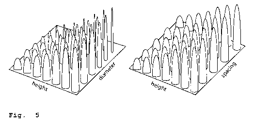
Fig. 5 shows a single substrate covered by nanopillars with
different height and diameter (left) and different height and
spacing (right).
Fig. 6 shows the basic principle of an optical device wherein
a beam of light passes through one aperture, a nanostructure
gradient filter (NGF) and another aperture.
Fig. 7 shows the basic principle of an optical device wherein
a rotating mirror is used to deflect a beam of light towards a
pre-selected region of a NGF.
Fig. 8 shows the basic principle of an optical device wherein
a movable light-source projects a beam of light into a prism
with at least one side covered by a NGF.
The following examples are used for more in depth explanation
of the present invention, without limiting the same thereto,
however. It will be evident for the person skilled in the art
that variations of these conditions in dependence of the
specific materials used may be required and can be determined
without difficulty by means of routine experiments.
EXAMPLE 1
Creation of a plurality of nanostructure gradients
on the same single substrate
1. Providing a composite substrate
A primary substrate, such as suprasil glass, is coated with at
least one layer of an easily RIE etchable material such as Si02
by means of sputter coating (UHV system; 99.995% Si02 target,
CA 02994503 2018-02-01
WO 2017/028948 PCT/EP2016/001387
18
3.00 inch diameter, 0.125 inch thickness, room temperature
sputter at 150W RF power with 02 and Ar at 2*10-3 mbar, base
pressure: 10-6 mbar).
By slowly tilting the substrate during the deposition process,
a gradient with varying thickness is deposited onto the
substrate. By selecting the appropriate deposition methods and
changing the tilting orientation during the deposition, it is
possible to create simple 2D gradient or more complex 3D
gradients (compare Fig. 2) with a linear or any other increase
of layer thickness.
2. Providing an array of nanoparticles on the substrate
surface
The surface of the graded "sacrificial" layer of the composite
substrate was coated with gold nanoparticles in a defined
arrangement by means of micellar nanolithography. In this
step, one of the protocols described in EP 1 027 157 Bl, DE
197 47 815 Al or DE 10 2007 017 032 Al can be followed.
The method involves the deposition of a micellar solution
of a block copolymer (e.g.
polystyrene(n)-b-poly(2-
vinylpyridine(m)) in toluene) onto the substrate, e.g. by
means of dip or spin coating, as a result of which an ordered
film structure of polymer domains is formed on the surface.
The micelles in the solution are loaded with a gold salt,
preferably HAuClei, which, following deposition with the polymer
film, can be reduced to the gold nanoparticles.
The reduction can take place chemically, e.g. with hydrazine,
or by means of energy-rich radiation, such as electron
radiation or light. Optionally, after or at the same time as
the reduction, the polymer film can be removed (e.g. by means
of plasma etching with Ar-, H- or 0-ions). Thereafter, the
CA 02994503 2018-02-01
WO 2017/028948 PCT/EP2016/001387
19
substrate surface is covered with an arrangement of gold
nanoparticles.
By using the BCML technology in combination with dip-coating
techniques it is possible to create gold-dots with different
spacing and diameter on the Si02 sacrificial layer (compare
Fig.3). By selecting the dipping-orientation of the substrate,
the BCML gradient can either be parallel or in any orientation
relative to the Si02 gradient on the substrate.
3. First Etching
Subsequently, the etching of the substrate surface covered
with gold nanoparticles took place in a desired depth. A
"reactive ion etcher" from Oxford Plasma, device: PlasmaLab 80
plus was used to this end. Other devices known in the prior
art are likewise fundamentally suitable, however. The etching
consisted of two treatment steps with various etchants which
were carried out several times one after the other.
The following protocol was used to create conical
nanostructures:
Step 1:
A mixture of Ar/SF6/02 in the ratio 10:40:8 (sccm) was used as
etchant (process gas).
Pressure: 50 mTorr
RF power: 120 W
ICP power: 0 W
Time: 60 s
Step 2:
Etchant: Ar/CHF3:40:40
Pressure: 50 mTorr
CA 02994503 2018-02-01
WO 2017/028948 PCT/EP2016/001387
RF power: 120 W
ICP power: 20 W
Time: 20 s
These 2 steps were carried out alternately 8 times.
Alternatively, the following protocol was used to create
pillar-shaped nanostructures:
Step 1:
A mixture of Ar/SF6 in the ratio 40:40 (sccm) was used as
etchant (process gas).
Pressure: 50 mTorr
RF power: 120 W
ICP power: 0 W
Time: 60 s
Step 2:
Etchant: Ar/CHF3:40:40
Pressure: 50 mTorr
RF power: 120 W
ICP power: 20 W
Time: 20 s
These 2 steps were carried out alternately 8 times.
The total duration of the etching treatment varied depending
on the desired depth of the etching within about 1-15 minutes.
As a result, column-like or conical nanostructures were
obtained, which still can show gold nanoparticles on their
upper side.
CA 02994503 2018-02-01
WO 2017/028948 PCT/EP2016/001387
21
4. Second Etching
The nanostructures created on the graded layer as outlined
above can further be used as an etching mask for transferring
said nanostructures into the primary substrate layer by means
of RIE or reactive ion beam etching (RIBE). Compared to the
RIE process described above, the RIBE procesa is less
selective and can etch substrates, which cannot be etched
using RIE.
Reactive ion beam etching (RIBE) uses an energetic, broad beam
collimated and highly directional ion source to physically
mill material from a substrate mounted on a rotating fixture
with adjustable tilt angle. In contrast to ion beaming (IBE),
in the RIBE process reactive ions are incorporated in whole or
in part in the etching ion beam.
The ion sources used are "gridded" ion sources, e.g. of the
Kaufman type or microwave electron cyclotron resonance (ECR).
The etching process involves the control of the ion incident
angle and a separate control of the ion flux and ion energy.
Typical reactive and inert gases used for RIBE are Ar, N2, 02,
CHF3 CF4 and SF6.
The RIE or RIBE process directly transferred the nanostructure
of the mediating sacrifical layer into the primary substrate.
EXAMPLE 2
Characterisation of nanostructured composite
or primary substrates
Suprasil samples with a gradient Si02 layer and electroless
treated BCML patterns were etched on one side using a RIE
process as described above. Wavelength-dependent transmittance
CA 02994503 2018-02-01
WO 2017/028948 PCT/EP2016/001387
22
was then measured using a spectrometer set-up with a beam size
of -1mm. After the measurements the samples were cleaved to
take SEM pictures of the pillar cross sections. Fig. 1A shows
the geometry of the pillar structure on one side of the sample
(-42nm diameter, 350nm height, Fig. 1B on the opposite side of
the same sample (-78nm diameter, 420nm height). Fig. 10 shows
the corresponding improved overall transmittance (compared to
a plain suprasil substrate) and the shift of the transmission
maximum.