Note: Descriptions are shown in the official language in which they were submitted.
CA 02994649 2018-02-02
DESCRIPTION
TITLE OF THE INVENTION:
RESIN OPTICAL WAVEGUIDE
TECHNICAL FIELD
[0001]
The present invention relates to a resin optical waveguide.
BACKGROUND ART
[0002]
Non-Patent Documents 1 and 2 and Patent Document I propose a silicon
photonics interface in which a silicon optical waveguide is connected to a
resin optical
waveguide with low loss and at low cost. The silicon optical waveguide
referred to in the
present Description has a core-clad structure that functions as a (single-
mode) optical
waveguide formed on a silicon chip.
FIG. 3 is a perspective view illustrating a configuration example of such a
silicon
photonics interface and FIG. 4 is a side view thereof.
In a resin optical waveguide chip 300 illustrated in FIGs. 3 and 4, one or a
plurality of resin optical waveguides 310 are formed. At one end side of the
resin optical
waveguide chip 300, the resin optical waveguide(s) 310 is (are) connected to a
silicon
optical waveguide (not illustrated) formed on a silicon optical waveguide chip
200.
Another end side of the resin optical waveguide chip 300 is housed in a
connector 100.
[0003]
FIG. 5 is a perspective view illustrating a configuration example of the resin
optical waveguide to be used for the above purpose.
The resin optical waveguide 310 illustrated in FIG. 5 has an under cladding
330
and an over cladding 340 provided around a core 320. However, the tip of the
side with
which the silicon optical waveguide (not illustrated) formed on the silicon
optical
waveguide chip 200 is to be connected in FIGs. 3 and 4 has no over cladding
340 provided,
and forms a core-exposed section 350 where the core 320 is exposed to the
outside.
[0004]
FIG. 6 is a cross-sectional view illustrating a connecting part between the
silicon
optical waveguide 210 and the resin optical waveguide 310 in the silicon
photonics
CA 02994649 2018-02-02
interface illustrated in FIGs. 3 and 4. The resin optical waveguide 310 is the
resin optical
waveguide 310 illustrated in FIG 5. In FIG 6, the silicon optical waveguide
210 and the
resin optical waveguide 310 are connected by using an epoxy resin in a state
that the core
320 of the resin optical waveguide 310 faces to the silicon optical waveguide
210.
[0005]
FIG. 7 is a schematic view for explaining light propagation in the silicon
photonics interface illustrated in FIGs. 3 and 4. In FIG. 7, light is
propagated from a core
220 of the silicon optical waveguide 210 to the core 320 exposed at the tip of
the resin
optical waveguide 310 by adiabatic coupling. Then, the light is propagated
from the core
320 of the resin optical waveguide 310 to a core 140 of an optical fiber 130.
PRIOR ART DOCUMENT
NON-PATENT DOCUMENT
[0006]
Non-Patent Document 1: Jie Shu, Ciyuan Qiu, Xuezhi Zhang, and Qianfan Xu,
"Efficient coupler between chip-level and board-level optical waveguides",
OPTICS
LETTERS, Vol. 36. No. 18, pp 3614-3616 (2011)
Non-Patent Document 2: Tymon Barwics, and Yoichi Taira, "Low-Cost
Interfacing of Fibers to Nanophotonic Waveguides: Design for Fabrication and
Assembly
Toleranes", IEEE Photonics Journal, Vol. 6, No. 4, August, 660818 (2014)
PATENT DOCUMENT
[0007]
Patent Document 1: US Patent No. 8,724,937
SUMMARY OF THE INVENTION
PROBLEMS THAT THE INVENTION IS TO SOLVE
[0008]
The resin optical waveguide 310 illustrated in FIG. 5 is subjected to
performance
evaluation with the same procedure as in the case of conventional resin
optical waveguide
before being mounted on the silicon photonics interface illustrated in FIGs. 3
and 4. In
the performance evaluation of the resin optical waveguide, a single-mode
optical fiber is
connected to a tip of the resin optical waveguide. FIG 8 is a schematic view
for
explaining light propagation in the case where a single-mode optical fiber is
connected to a
tip of the resin optical waveguide 310 illustrated in FIG 5. In the connection
of the resin
optical waveguide 310 illustrated in FIG 5 and the single-mode optical fiber
400, a part of
CA 02994649 2018-02-02
the light is emitted from the portion at which the core 320 at the tip of the
resin optical
waveguide 310 is exposed and is not propagated, and also there is a problem
where
connection loss occurs. This connection loss does not occur at the time of
mounting on
the silicon photonics interface illustrated in FIGs. 3 and 4 and thus, lowers
the reliability of
.. the results of the performance evaluation.
[0009]
In order to solve the problems of the conventional art described above, an
object
of the present invention is to provide a resin optical waveguide which is
suitable for the use
in a silicon photonics interface in which a silicon optical waveguide is
connected to the
resin optical waveguide with low loss and at low cost, and which exhibits high
reliability
of performance evaluation using a single-mode optical fiber.
MEANS FOR SOLVING THE PROBLEMS
[0010]
In order to achieve the object described above, the present invention provides
a
resin optical waveguide containing a core, an under cladding and an over
cladding having
refractive indices lower than that of the core,
in which the resin optical waveguide has, at one end side thereof, a core-
exposed
section at which the over cladding is not present and the core and the under
cladding
nearby the core are exposed and,
of the under cladding, a portion corresponding to the core-exposed section has
a
first layer and a second layer that satisfy the following (1) to (3):
(1) the first layer and the second layer differ from each other in a
distance from an
interface with the core or an exposed surface of the under cladding, and the
first layer is
positioned on a near side to these surfaces and the second layer is positioned
on a far side
from these surfaces;
(2) the first layer is positioned within 151.1.1T1 in the distance from the
interface with
the core or the exposed surface of the under cladding; and
(3) the first layer and the second layer differ from each other in
refractive index, and
the first layer has the refractive index higher than that of the second layer.
[0011]
In the resin optical waveguide of the present invention, the core-exposed
section
has a length of preferably 100 pm or more in a light propagation direction.
[0012]
CA 02994649 2018-02-02
4
The resin optical waveguide of the present invention preferably has a
difference
(ni,max-n2,..) between the maximum value ni,ma, of the refractive index of the
first layer
and the maximum value n2,max of the refractive index of the second layer being
0.001 or
more.
[0013]
In the resin optical waveguide of the present invention, the first layer has a
thickness t of preferably 15 1.tm or less.
[0014]
The resin optical waveguide of the present invention preferably has a product
(tx(ni,max-nzmax)) of the thickness t of the first layer and the difference
(ni,max-nzmax)
between the maximum value ni,max of the refractive index of the first layer
and the
maximum value n2,max of the refractive index of the second layer being from
0.001 to 0.2
[0015]
The resin optical waveguide of the present invention preferably has a
difference
(ri,max-ni,max) between the maximum value n.,max of the refractive index of
the core and the
maximum value ni,max of the refractive index of the first layer being from
0.008 to 0.02.
[0016]
In the resin optical waveguide of the present invention, the under cladding
has a
thickness of preferably 10 iim or more.
[0017]
The resin optical waveguide of the present invention is preferably a single-
mode
optical waveguide at a wavelength of at least one of 1,310 nm and 1,550 nm.
[0018]
In the resin optical waveguide of the present invention, the resin optical
waveguide has a core size of preferably from 1 to 10 m.
[0019]
In the resin optical waveguide of the present invention, the core of the resin
optical waveguide is preferably composed of a resin containing fluorine.
[0020]
Moreover, the present invention provides a resin optical waveguide containing
a
core, an under cladding having a refractive index lower than that of the core
and an over
cladding,
84183398
in which the resin optical waveguide has, at one end side thereof, a core-
exposed section at
which the over cladding is not present and the core and the under cladding
nearby the core are exposed is
provided, and the core-exposed section has a length of 500 pm or more in a
light propagation direction
of the resin optical waveguide and,
5 of the under cladding, a portion corresponding to the core-exposed
section has a
first layer and a second layer that satisfy the following (1) to (4):
(1) the first layer and the second layer differ from each other in a
distance from an interface with the
core or an exposed surface of the under cladding, and the first layer is
positioned on a near side to these
surfaces and the second layer is positioned on a far side from these surfaces;
(2) the first layer is positioned within 8p.m in the distance from the
interface with the core or the
exposed surface of the under cladding;
(3) the first layer and the second layer differ from each other in
refractive index, and the first layer
has a refractive index higher than that of the second layer; and
(4) a difference (nt,max-n2,.) between the maximum value ni,m of the
refractive index of the first
layer and the maximum value n2,. of the refractive index of the second layer
is 0.002 or more.
[0021]
The resin optical waveguide of the present invention is preferably connected
with a silicon
optical waveguide at the core-exposed section.
[0021a]
Some embodiments disclosed herein may provide a resin optical waveguide
comprising a core,
an under cladding and an over cladding having refractive indices lower than
that of the core, wherein the
resin optical waveguide comprises, at one end side thereof, a core-exposed
section at which the over
cladding is not present and the core and the under cladding nearby the core
are exposed and, of the under
cladding, a portion corresponding to the core-exposed section comprises a
first layer and a second layer
that satisfy the following (1) to (5): (1) the first layer and the second
layer differ from each other in a
distance from an interface with the core or an exposed surface of the under
cladding, and the first layer is
positioned on a near side to these surfaces and the second layer is positioned
on a far side from these
surfaces; (2) the first layer is positioned within 15 )1m in the distance from
the interface with the core or
the exposed surface of the under cladding; (3) the first layer and the second
layer differ from each other
in refractive index, and the first layer has the refractive index higher than
that of the second layer; (4) a
difference (n1,max-n2,max) between a maximum value ni,max of the refractive
index of the first layer and a
Date Regue/Date Received 2023-01-09
84183398
5a
maximum value fl2,max of the refractive index of the second layer is from
0.005 to 0.015; and (5) the first
layer has a thickness t of 6 gm or less.
[0021b]
Some embodiments disclosed herein may provide a resin optical waveguide
comprising a core,
an under cladding and an over cladding having refractive indices lower than
that of the core, wherein the
resin optical waveguide comprises, at one end side thereof, a core-exposed
section at which the over
cladding is not present and the core and the under cladding nearby the core
are exposed, and the core-
exposed section has a length of 500 gm or more in a light propagation
direction of the resin optical
waveguide and, of the under cladding, a portion corresponding to the core-
exposed section comprises a
first layer and a second layer that satisfy the following (1) to (5): (1) the
first layer and the second layer
differ from each other in a distance from an interface with the core or an
exposed surface of the under
cladding, and the first layer is positioned on a near side to these surfaces
and the second layer is
positioned on a far side from these surfaces; (2) the first layer is
positioned within 8 gm in the distance
of from the interface with the core or the exposed surface of the under
cladding; (3) the first layer and
the second layer differ from each other in refractive index, and the first
layer has a refractive index
higher than that of the second layer; (4) a difference between a maximum
value ni,m of
the refractive index of the first layer and a maximum value nzmax of the
refractive index of the second
layer is 0.005 to 0.015; and (5) the first layer has a thickness t of 6 gm or
less.
ADVANTAGEOUS EFFECT OF THE INVENTION
[0022]
The resin optical waveguide of the present invention is suitable for the use
in a
silicon photonics interface in which a silicon optical waveguide is connected
to a resin
optical waveguide with low loss and at low cost.
The resin optical waveguide of the present invention exhibits low connection
loss during
performance evaluation using a single-mode optical fiber and thus the
performance evaluation is highly
reliable.
BRIEF DESCRIPTION OF DRAWINGS
[0023]
[FIG 1] FIG 1 is a perspective view illustrating a configuration example of
the resin optical
waveguide of the present invention.
Date Regue/Date Received 2023-01-09
CA 02994649 2018-02-02
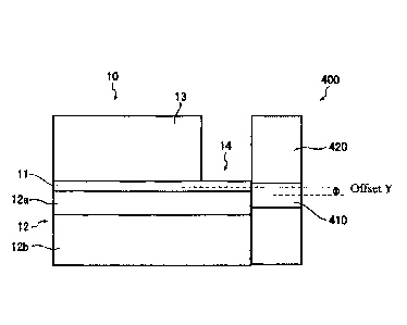
[FIG 2] FIG 2 is a schematic view illustrating a connecting part between a
resin
optical waveguide and a single-mode optical fiber in Examples.
[FIG 3] FIG. 3 is a perspective view illustrating a configuration example of a
silicon photonics interface.
[FIG 4] FIG 4 is a side view of the silicon photonics interface of FIG 3.
[FIG 5] FIG. 5 is a perspective view illustrating a configuration example of
the
resin optical waveguide for use in the silicon photonics interface of FIGs. 3
and 4.
[FIG 6] FIG. 6 is a cross-sectional view illustrating a connecting part
between a
silicon optical waveguide and a resin optical waveguide 310 formed on a
silicon optical
waveguide chip 200 in the silicon photonics interface illustrated in FIGs. 3
and 4.
[FIG 7] FIG 7 is a schematic view for explaining light propagation in the
silicon photonics interface illustrated in FIGs. 3 and 4.
[FIG 8] FIG. 8 is a schematic view for explaining light propagation when a
single-mode optical fiber is connected to the tip of the resin optical
waveguide 310
illustrated in FIG. 5.
MODE FOR CARRYING OUT THE INVENTION
[0024]
The following will explain the present invention with reference to Drawings.
FIG. 1 is a perspective view illustrating a configuration example of the resin
optical waveguide of the present invention. The resin optical waveguide 10
illustrated in
FIG 1 contains a core 11, an under cladding 12 having a refractive index lower
than that of
the core 11 and an over cladding 13 also having a refractive index lower than
that of the
core 11. The under cladding 12 is provided under the core 11 and the over
cladding 13 is
provided over the core 11. However, a core-exposed section 14 at which the
over
cladding 13 is not present and the core 11 is exposed is provided at one end
side of the
resin optical waveguide 10.
In the resin optical waveguide of the present invention, of the under cladding
and
over cladding provided around the core, the one that is not present at the
core-exposed
section is regarded as the over cladding. Therefore, the under cladding may be
provided
over the core and the over cladding may be provided under the core.
[0025]
The core-exposed section 14 is to be a connecting portion with a silicon
optical
waveguide when the resin optical waveguide 10 is used in a silicon photonics
interface.
CA 02994649 2018-02-02
Therefore, the core-exposed section 14 is required to have a sufficient length
for the use as
the connecting portion with the silicon optical waveguide. In the resin
optical waveguide
of the present invention, the length of the core-exposed section 14 in a light
propagation
direction of the resin optical waveguide is preferably 100 tun or more, which
is a sufficient
5 length for the use as the connecting portion with the silicon optical
waveguide.
Incidentally, the light propagation direction of the resin optical waveguide
is the long axis
direction of the core 11.
In the core-exposed section 14, the length in the light propagation direction
of the
resin optical waveguide is more preferably 300 p.m or more, further preferably
500 pm or
10 more, and even further preferably 1,000 lam or more.
However, in the case where the length of the core-exposed section 14 in the
light
propagation direction of the resin optical waveguide is too long, there is a
concern that the
connection loss may increase when connecting with a silicon optical waveguide
by using
an adhesive (e.g., an epoxy resin), due to absorption of the adhesive.
Therefore, the
length of the core-exposed section 14 in the light propagation direction of
the resin optical
waveguide is preferably 10,000 p.m or less, more preferably 5,000 p.m or less,
and further
preferably 3,000 vim or less.
[0026]
In the resin optical waveguide 10, the refractive indices of the under
cladding 12
and the over cladding 13 are made lower than that of the core 11 for
preventing the light
propagated through the core 11 from emitting to the under cladding 12 side or
to the over
cladding 13 side.
As mentioned above, when the resin optical waveguide 310 having the
core-exposed section is connected to the single-mode optical fiber 400 as
illustrated in FIG.
8, the core 320 is in an exposed state at the core-exposed section where the
over cladding
340 is not present. Since the performance evaluation of the resin optical
waveguide 310
is performed under a condition that the core-exposed section is present in air
or in water,
the exposed surface of the core 320 comes into contact with air or water. But
air or water
has a refractive index smaller than those of the materials of the core 320 and
the under
cladding 330 of the resin optical waveguide 310. As a result, a part of the
light
propagated through the core 320 is emitted to the under cladding 330 side,
which is a cause
of the connection loss.
CA 02994649 2018-02-02
a
In the resin optical waveguide 10 of the present invention, of the under
cladding
12, the portion corresponding to the core-exposed section 14 has a first layer
and a second
layer, which satisfy the following (1) to (3). Therefore, the connection loss
at the time of
connection with a single-mode optical fiber is suppressed:
(1) the first layer and the second layer differ from each other in distance
from the
interface with the core or the exposed surface of the under cladding, and the
first layer is
positioned on a near side to these surfaces and the second layer is positioned
on a far side
from these surfaces;
(2) the first layer is positioned within 15 pm in the distance from the
interface with
the core or the exposed surface of the under cladding;
(3) the first layer and the second layer differ from each other in
refractive index, and
the first layer has a refractive index higher than that of the second layer.
[0027]
As suggested in the above (1), of the under cladding 12, the portion
corresponding
to the core-exposed section 14 has a bilayer structure in which the near side
to the interface
with the core 11 or the exposed surface of the under cladding 12 is the first
layer and the
far side from these surfaces is the second layer. Incidentally, the interface
with the core
11 and the exposed surface of the under cladding 12 form a part of the first
layer.
As suggested in the above (3), the first layer has a refractive index higher
than that
of the second layer. Such a bilayer structure suppresses the emission of the
light
propagated through the core 11 to the under cladding 12 side in the core-
exposed section
14 and thus, suppresses the connection loss at the time of the connection with
a
single-mode optical fiber.
[0028]
As suggested in the above (2), the first layer is positioned within 15 im in a
distance from the interface with the core 11 or the exposed surface of the
under cladding
12. Therefore, the thickness t of the first layer is 15 pm or less. The
reason why the
distance from the interface with the core 11 or the exposed surface of the
under cladding
12 is controlled to 15 tm or less is as follows.
In the case where the distance from the interface with the core 11 or the
exposed
surface of the under cladding 12 is controlled to 15 p.m or less, the emission
of the light
propagated through the core 11 to the under cladding 12 side is suppressed and
thus the
CA 02994649 2018-02-02
connection loss at the time of the connection with a single-mode optical fiber
is
suppressed.
In the first layer, the distance from the interface with the core 11 or the
exposed
surface of the under cladding 12 is preferably 10 gm or less, more preferably
8 gm or less,
and further preferably 6 gm or less. Therefore, the thickness t of the first
layer is
preferably 10 gm or less, more preferably 8 p.m or less, and further
preferably 6 p.m or less.
However, in the first layer, too small distance from the interface with the
core 11
or the exposed surface of the under cladding 12 makes insufficient the
suppression of the
emission of the light propagated through the core 11 to the under cladding 12
side. In the
first layer, the distance from the interface with the core 11 or the exposed
surface of the
under cladding 12 is preferably 0.1 p.m or more, more preferably 0.2 p.m or
more, and
further preferably 0.5 p.m or more. Therefore, the thickness t of the first
layer is
preferably 0.1 gm or more, more preferably 0.2 gm or more, and further
preferably 0.5 p.m
or more.
[0029]
In order to suppress the connection loss at the time of the connection with a
single-mode optical fiber, the difference (ni,max-n2,max) between the maximum
value ni,max
of the refractive index of the first layer and the maximum value n2,.ax of the
refractive
index of the second layer is preferably 0.001 or more. fll,maxfl2,max being
0.001 or more
provides the aforementioned effect of suppressing the connection loss at the
time of the
connection with a single-mode optical fiber, preferably. ni,max-n2,max is
preferably 0.002
or more and more preferably 0.004 or more.
Incidentally, an upper limit value of the difference (ni,max-n2,max) between
the
maximum value fll,max of the refractive index of the first layer and the
maximum value
112,max of the refractive index of the second layer is not particularly
limited but, for example,
may be set to 0.020 owing to the production method or the like to be mentioned
later.
Here, the difference between the maximum value ni,max of the refractive index
of
the first layer and the maximum value n2,,,m, of the refractive index of the
second layer is
used because a case where the first layer and the second layer are each
separated into a
plurality of layers having different refractive indices each other is
considered. In this
case, it is required for the plurality of layers constituting the first layer
and the plurality of
layers constituting the second layer that a nearer side to the interface with
the core or the
exposed surface of the under cladding has a higher refractive index and a
farther side from
CA 02994649 2018-02-02
1
these surfaces has a lower refractive index. Moreover, it is required for the
plurality of
the layers constituting the first layer that the largest value of the
difference in the refractive
indices is less than 0.001.
[0030]
In order to suppress the connection loss at the time of connection with a
single-mode optical fiber, the product (tx(ni,max-nzmax)) of the thickness t
of the first layer
and the difference (ni,max-n2,,a.) between the maximum value nimia, of the
refractive index
of the first layer and the maximum value n2,max of the refractive index of the
second layer is
preferably from 0.001 to 0.2 p.m. The product is more preferably from 0.004 to
0.15 1.1m
and particularly preferably from 0.004 to 0.12 p.m.
[0031]
In view of suppression of the connection loss with a silicon optical waveguide
and
suppression of the connection loss at the time of connecting with a single-
mode optical
fiber, the difference (n'max-nniax) between the maximum value rim, of the
refractive index of
the core 11 and the maximum value nm of the refractive index of the first
layer is
preferably from 0.008 to 0.02. Here, the maximum value lima, of the refractive
index of
the core 11 is used because a case where refractive index distribution is
present also in the
core 11 is considered.
nn,ax-nmax is more preferably from 0.010 to 0.015.
[0032]
The thickness of the under cladding 12 is preferably 10 p.m or more in order
to
increase rigidity and improve easiness of handling. The thickness of the under
cladding
12 is more preferably 15 p.m or more and further preferably 20 pm or more. In
the case
where the under cladding 12 is composed of the first layer and the second
layer, the
emission of light can be suppressed in any thickness as long as the second
layer has a
refractive index lower than that of the first layer. The thickness is
preferably 70 p.m or
less and further preferably 50 p.m or less in terms of productivity.
[0033]
In the resin optical waveguide of the present invention, the refractive index
of the
under cladding 12 at the portion where the over cladding 13 and the under
cladding 12 are
provided over and under the core 11 is not particularly limited as long as the
numerical
value is lower than the refractive index of the core 11. Therefore, for
example, the under
cladding 12 at the portion may have a refractive index of an equal numerical
value as a
CA 02994649 2018-02-02
11
whole, or may have a portion where the refractive index is different between
at the near
side and at the far side with respect to the core 11. However, such a portion
is required to
have a higher refractive index at the near side to the core 11 and a lower
refractive index at
the far side from the core 11. Furthermore, the portion may have the same
configuration
= 5 as the first layer and the second layer which satisfy the above (1)
to (3).
[0034]
The resin optical waveguide of the present invention will be further
described.
(Core 11)
In the resin optical waveguide 10 illustrated in FIG 1, the cross-sectional
shape of
the core 11 is rectangular, but the shape is not limited thereto and may be,
for example,
trapezoidal, circular or elliptic. In the case where the cross-sectional shape
of the core 11
is polygonal, the corners may be rounded.
[0035]
The core size is not particularly limited and can be appropriately designed in
consideration of a light source, coupling efficiency with a light receiving
element, or the
like. The coupling efficiency depends on the core diameter and the numerical
aperture
(NA). For example, the core size (in the case where the cross-sectional shape
of the core
11 is rectangular as in the case of the core 11 illustrated in FIG. 1, width
and height of the
rectangle) of the core 11 is preferably from 1 to 10 gm in terms of the
coupling efficiency
with a silicon optical waveguide to be connected at the time of the use in a
silicon
photonics interface. The core size is more preferably from 1.5 to 8 gm and
further
preferably from 2 to 7 gm. Here, the width of the rectangle is the length of
the width at
the central position of the height and the height of the rectangle is the
length of the height
at the central position of the width. Incidentally, the core size may change
in a tapered
manner along the light propagation direction of the resin optical waveguide.
[0036]
The core 11 may have such refractive index distribution that the refractive
index
decreases toward the far side with respect to the center of the core. Also,
the core may
have such refractive index distribution that the refractive index at the over
cladding side is
higher and the refractive index at the under cladding side is lower or such
refractive index
distribution that the refractive index at the over cladding side is lower and
the refractive
index at the under cladding side is higher.
CA 02994649 2018-02-02
112
=
Here, the maximum value n'ma,, of the refractive index of the core 11 is used
because, for example, as mentioned above, the case where refractive index
distribution is
present also in the core 11 is considered.
[0037]
(Over cladding 13)
The over cladding 13 is not particularly limited as long as it has a
refractive index
lower than that of the core 11. Therefore, the over cladding 13 may have a
refractive
index of an equal numerical value as a whole. Alternatively, the over cladding
13 may
have a portion where the refractive indices are different between at the near
side and at the
far side with respect to the core 11. In this case, the over cladding 13 may
have a
configuration where the refractive index decreases toward the far side with
respect to the
core 11 or may have a configuration where the refractive index increases
toward the far
side with respect to the core 11.
The thickness of the over cladding 13 is not particularly limited. However, in
the
case where the resin optical waveguide 10 of the present invention is a single-
mode optical
waveguide, a propagated light leaks also to the clad part existing within the
range of about
10 m from the center of the core 11. Therefore, the thickness is preferably
10 1.1.m or
more from the viewpoint of decreasing the propagation loss of light. Moreover,
the total
thickness of the under cladding 12 and the over cladding 13 is preferably from
20 to 90 pm
and more preferably from 30 to 70 p.m.
[0038]
In the resin optical waveguide of the present invention, constituting
materials of
the core 11, the under cladding 12 and the over cladding 13 are not
particularly limited as
long as they satisfy the required properties as the resin optical waveguide.
However, the
constituting material of the core 11 is preferably a resin containing fluorine
in view of
suppressing the loss of the light propagated through the core 11.
Moreover, with regard to the constituting materials of the core 11, the under
cladding 12 and the over cladding 13 and the production procedures of the
resin optical
waveguide, for example, the descriptions in the following literatures can be
referenced.
W02010/107005
JP-A-2013-120338
JP-A-2012-63620
[0039]
CA 02994649 2018-02-02
13
In the case where the resin optical waveguide 10 of the present invention
illustrated in FIG. 1 is produced with reference to the above literatures, the
core-exposed
section 14 of the resin optical waveguide 10 can be formed by the following
procedure.
An under cladding is formed and a core is formed on the under cladding by
using
a photolithography process. And then, a curable composition is applied on the
under
cladding and the core and the curable resin composition is cured by heating
and/or light
irradiation to form an over cladding. At the time of forming the over cladding
layer, a
region having the over cladding and a region where the over cladding is absent
and the
core is exposed (i.e., a core-exposed section) can be formed by using a
photolithography
process.
[0040]
Furthermore, the under cladding 12 having a first layer 12a and a second layer
12b which satisfy the above (1) to (3) can be formed by the following
procedure.
The under cladding 12 having the first layer 12a and the second layer 12b can
be
formed by adjusting heating temperature and heating time and/or by adjusting
irradiation
intensity and irradiation time of light at the time of forming the under
cladding as above.
Alternatively, the under cladding 12 having the first layer 12a and the second
layer 12b can
be formed by adding a dopant for adjusting the refractive index. Also, the
under cladding
12 having the first layer 12a and the second layer 12b can be formed by
applying a curable
composition (b) to form the under cladding 12b, performing heating and/or
light irradiation
to cure the composition, applying a curable composition (a) to form the under
cladding 12a
thereon, and performing heating and/or light irradiation to cure the
composition. For the
curable composition (a) and the curable composition (b), materials described
in the
above-mentioned literatures can be appropriately used.
In the case where the refractive index is adjusted by dopant addition, the
refractive
index depends on the material constituting the under cladding and the kind of
the dopant.
Therefore, the dopant is appropriately selected depending on the material
constituting the
under cladding to obtain the target refractive index.
[0041]
For the use in a silicon photonics interface in which a silicon optical
waveguide is
connected to an optical fiber with low loss and at low cost, the resin optical
waveguide of
the present invention is preferably a single-mode optical waveguide since
optical signals
can be highly densified. In this case, the resin optical waveguide is
preferably the
single-mode optical waveguide at a wavelength of at least one of 1,310 nm and
1,550 nm
CA 02994649 2018-02-02
1.4
=
since it can propagate light also to a silicon optical waveguide and a single-
mode optical
fiber with low loss.
[0042]
In the case where the resin optical waveguide of the present invention is used
in a
.. silicon photonics interface, the resin optical waveguide is connected with
the silicon
optical waveguide at the core-exposed section thereof.
EXAMPLES
[0043]
The following will describe the present invention in further detail with
reference
to Examples but the present invention should not be construed as being limited
to these
Examples.
[0044]
In Examples described below, the structures (size and refractive index) of a
resin
optical waveguide and a single-mode optical fiber were defined by RSoft CAD
manufactured by RSoft Design Group Inc. and simulation of light propagation
was
performed by BeamProp (finite difference beam propagation method) that is a
simulation
engine manufactured by RSoft Design Group Inc. FIG. 2 is a schematic view
illustrating
a connecting part between the resin optical waveguide and the single-mode
optical fiber in
Examples.
[0045]
(Examples 1 to 40)
Of Examples 1 to 40, Examples 1 to 7, 9 to 23, and Examples 25 to 40 are
Working Examples and each under cladding 12 had a bilayer structure of a first
layer and a
second layer. Example 8 and Example 24 are Comparative Examples and each under
cladding had a structure of a first layer alone.
The structures of the resin optical waveguide and the single-mode optical
fiber
were defined by RSoft CAD as shown below.
[0046]
(Single-mode optical fiber 400)
Core 410
Core diameter: 8.41.tm
Refractive index: 1.47
Clad 420
CA 02994649 2018-02-02
13
Clad diameter: 80 p.m
Refractive index: 1.4652
[0047]
(Resin optical waveguide 10)
Single-mode optical waveguide
Core 11
Core size: 5.9 jim in the width direction, 2.3 p.m in the longitudinal
direction
Refractive index: 1.534
Under cladding 12
Thickness: 40 pm
First layer 12a
Refractive index: 1.52
Thickness t: 2 to 14 p.m
Second layer 12b
Difference in refractive index between the first layer 12a and the second
layer 12b: 0 to 0.015
In Example 8 and Example 24, the under cladding 12 does not have a bilayer
structure and the refractive index of the whole under cladding 12 is 1.52.
Over cladding 13
Refractive index: 1.52
Thickness: 40 p.m
Core-exposed section 14
Length in the light propagation direction of the resin optical waveguide 10:
2,000
p.m
Under a condition that the core-exposed section 14 was filled with water
(refractive index: 1.32) or air (refractive index: 1.00), connection loss at a
wavelength of
1.55 p.m was determined through calculation by BeamProp. The results are shown
in the
following tables. In the tables, of the refractive index (ni-n2), the
refractive index of the
first layer 12a is denoted as ni and the refractive index of the second layer
12b is denoted
as 112. The thickness in the tables is thickness of the first layer 12a.
Moreover, offset Y
between the core 11 of the optical waveguide 10 and the core 410 of the single-
mode
optical fiber 400 is as illustrated in FIG 2. The index in the tables is as
shown in the
following table.
CA 02994649 2018-02-02
1
[0048]
[Table 1]
Table 1
Index Connection loss
5 dB or less
4 more than 5 dB, 10 dB or less
3 more than 10 dB, 15 dB or less
2 more than 15 dB, 20 dB or less
1 more than 20 dB
5 [0049]
[Table 2]
Table 2
Ex. 1 Ex. 2 Ex. 3 Ex. 4 Ex. 5 Ex. 6 Ex. 7 Ex. 8
Difference in refractive
0.002 0.020 0.020 0.005 0.005 0.005 0.005 0.000
index (ni-n2)
Thickness t of first layer
2.0 4.0 6.0 2.0 6.0 10.0 14.0 0.0
(11m)
(ni-n2)xthicicriess t (m) 0.004 0.080 0.120 0.010 0.030 0.050 0.070 0.000
Condition of
water water water water water water water water
core-exposed section
Connection loss (dB) 4.7 5.0 5.7 4.4 4.9 7.1 13.4 -
>30
Index 5 5 4 5 5 4 3 1
[0050]
[Table 3]
CA 02994649 2018-02-02
17
Table 3
Ex. 9 Ex. 10 Ex. 11 Ex. 12 Ex. 13 Ex. 14 Ex. 15 Ex. 16
Difference in refractive
0.010 0.010 0.010 0.010 0.015 0.015 0.015 0.015
index (ni-n2)
Thickness t of first layer
2.0 4.0 6.0 8.0 2.0 4.0 6.0 8.0
(11m)
(ni-n2)xthickness t (j.1m) 0.020 0.040 0.060 0.080 0.030 0.060 0.090 0.120
Condition of
water water water water water water water water
core-exposed section
Connection loss (dB) 4.6 4.4 4.7 5.4 4.8 4.4 4.6
5.3
Index 5 5 5 4 5 5 5 4
[0051]
[Table 4]
Table 4
Ex. 17 Ex. 18 Ex. 19 Ex. 20 Ex. 21 Ex. 22 Ex. 23 Ex. 24
Difference in refractive
0.002 0.020 0.020 0.005 0.005 0.005 0.005 0.000
index (ni-n2)
Thickness t of first layer
2.0 4.0 6.0 2.0 6.0 10.0 14.0 0.0
(un)
(ni-n2)xthickness t (pm) 0.004 0.080 0.120 0.010 0.030 0.050 0.070 0.000
Condition of
air air air air air air air air
core-exposed section
Connection loss (dB) 7.6 6.6 7.8 5.0 6.1 11.3 18.5
>30
Index 4 4 4 5 4 3 2 1
[0052]
[Table 5]
CA 02994649 2018-02-02
18
Table 5
Ex. 25 Ex. 26 Ex. 27 Ex. 28 Ex. 29 Ex. 30 Ex. 31 Ex. 32
Difference in refractive
0.010 0.010 0.010 0.010 0.015 0.015 0.015 0.015
index (ni-n2)
Thickness t of first layer
2.0 4.0 6.0 8.0 2.0 4.0 6.0
8.0
(11m)
(ni-n2)xthickness t (um) 0.020 0.040 0.060 0.080 0.030 0.060 0.090 0.120
Condition of
air air air air air air air
air
core-exposed section
Connection loss (dB) 5.1 5.0 5.7 7.3 5.3 5.0 5.5
7.0
Index 4 5 4 4 4 5 4 4
[0053]
[Table 6]
Table 6
Ex. 33 Ex. 34 Ex. 35- Ex. 36 Ex. 37 Ex. 38 Ex. 39 Ex. 40
Difference in refractive
0.005 0.005 0.005 0.005 0.005 0.005 0.005 0.005
index (ni-n2)
Thickness t of first layer
4.0 4.0 4.0 4.0 4.0 4.0 4.0
4.0
(11m)
(ni-n2)xthickness t (pm) 0.020 0.020 0.020 0.020 0.020 0.020 0.020 0.020
Condition of
water water water water air air air air
core-exposed section
Offset Y (um) 0 2 4 6 0 2 4 6
Connection loss (dB) 4.5 3.3 4.2 6.8 5.2 3.7 4.2
6.4
Index 5 5 - 5 4 4 5 5 4
[0054]
The above Tables 1 to 6 show Examples where the length of the core-exposed
section 14 in the light propagation direction was set to 2,000 p,m. Table 7
and Table 8
below show results of Examples where the length of the core-exposed section 14
was set to
500 um, 1,000 um, 1,500 um, or 3,000 um.
[0055]
CA 02994649 2018-02-02
19
[Table 7]
Table 7
Ex. 41 Ex. 42 Ex. 43 Ex. 44 Ex. 45 Ex. 46 Ex. 47 Ex. 48
Difference in refractive
0.005 0.005 0.005 0.005 0.005 0.005 0.005 0.005
index (ni-n2)
Thickness t of first layer
4.0 4.0 4.0 4.0 4.0 4.0 4.0
4.0
(Pm)
(ni-n2)xthickness t (pm) 0.020 0.020 0.020 0.020 0.020 0.020 0.020 0.020
Condition of
air air air air air air air
air
core-exposed section
Length of core-exposed
500 500 500 500 1000 1000 1000 1000
section (1.1,m)
Offset Y (pm) 0 2 4 6 0 2 4 6
Connection loss 5.1 3.8 4.5 6.9 5.2 3.8 4.4
6.7
Index 4 5 5 4 4 5 5 4
[0056]
[Table 8]
Table 8
Ex. 49 Ex. 50 Ex. 51 Ex. 52 Ex. 53 Ex. 54 Ex. 55 Ex. 56
Difference in refractive
0.005 0.005 0.005 0.005 0.005 0.005 0.005 0.005
index (ni-n2)
Thickness t of first layer
4.0 4.0 4.0 4.0 4.0 4.0 4.0
4.0
(Pm)
(ni-n2)xthickness t (p.m) 0.020 0.020 0.020 0.020 0.020 0.020 0.020 0.020
Condition of
air air air air air air air
air
core-exposed section
Length of core-exposed
1500 1500 1500 1500 3000 3000 3000 3000
section (1.1m)
Offset Y (pin) 0 2 4 6 0 2 4 6
Connection loss 5.2 3.7 4.3 6.5 5.1 3.7 4.2
6.4
Index 4 5 5 4 4 5 5 4
84183398
[0057]
As is apparent from Tables, connection loss was large in Examples 8 and 24
where the under cladding 12 did not have a bilayer structure.
On the other hand, the connection loss was small in Examples 1 to 7, Examples
9
5 to 23, and Examples 25 to 56 where the under cladding 12 had a bilayer
structure.
Especially, the connection loss was small in Examples 1 to 7, Examples 9 to
23, and
Examples 25 to 56 where the bilayer structure had a difference in refractive
index (nl-n2)
of 0.001 or more.
In each of Examples 1 to 7, Examples 9 to 23, and Examples 25 to 32, the
product
10 (tx(nl-n2)) of the thickness t of the first layer and the difference (n1
-n2) between the
refractive index n1 in the first layer and the refractive index n2 in the
second layer satisfied
from 0.001 to 0.2 gm. Moreover, as shown in Table 6, in both cases of the
condition that
the core-exposed section 14 is filled with water and the condition that it is
filled with air,
when the difference (nl-n2) in refractive index between the first layer 12a
and the second
15 layer 12b is 0.001 or more, the influence of the offset Y between the
core 14 of the optical
waveguide 10 and the core 410 of the single-mode optical fiber 400 is small
regardless of
the difference (n1 -n1) in refractive index between the first layer 12a and
the second layer
12b.
[0058]
20 The present invention is described in detail with reference to specific
embodiments, but it is apparent for those skilled in the art that various
changes or
modifications can be added without departing from the spirit and the scope of
the present
invention. This application is based upon Japanese Patent Application (No.
2015-154192),
filed on August 4, 2015.
DESCRIPTION OF REFERENCE NUMERALS AND SIGNS
[0059]
10: Resin optical waveguide
11: Core
12: Under cladding
12a: First layer,
12b: Second layer
13: Over cladding
Date Recue/Date Received 2023-01-09
CA 02994649 2018-02-02
21
14: Core-exposed section
100: Connector
200: Silicon optical waveguide chip
210: Silicon optical waveguide
220: Core
230: Coating
300: Resin optical waveguide chip
310: Resin optical waveguide
320: Core
330: Under cladding
340: Over cladding
350: Core-exposed section
400: Single-mode optical fiber