Note: Descriptions are shown in the official language in which they were submitted.
A SYSTEM AND METHOD FOR DIRECT-SAMPLE EXTREMELY WIDE BAND
TRANSCEIVER
[0001]
TECHNICAL FIELD
[0002] This disclosure relates generally to radios, and in particular but not
exclusively,
relates to wide band, high dynamic range direct-sample transceivers.
BACKGROUND INFORMATION
[0003] Radios are traditionally based on super-heterodyne architecture. The
super-
heterodyne architecture, however, is complex and is only amenable to one small
band of frequencies
at a time, e.g., a spectral window. The complexity is due in part to the
addition of mixers and
various operational frequencies along with the inclusion of filters to
suppress unwanted signals
outside the desired spectral window. While conventional radios work well and
provide robust
communication systems, the ability to use a single radio for wider bands and
to reduce the
complexity of radios is highly desirable.
[0004] The desire for replacement radios that meet the goals of complexity
reduction and
high bandwidth has led to direct-sampling, wide band radios. The development
of the direct-
sampling, wide band radios has been predicated on the advances in analog-to-
digital converter
technology, as well as digital-to-analog converters. These radios, however,
suffer when in-band
strong signals drown out the weaker signals, which reduces the dynamic range
of the radio, and have
only operated as desired in controlled environments. Additionally, very high
speed analog-to-digital
converters have limited precision (8 to 10 bits), which suffices for strong
signals, but hinders the
detection and sampling of weak signals in the presence of strong signals.
1
CA 2997183 2019-08-19
SUMMARY
10004a1 According to one aspect there is provided a transceiver, comprising: a
first antenna
to receive an input signal, wherein the input signal is an RF signal spanning
a wide band of
frequencies and including weak signals and a strong signal; a first analog to
digital converter (ADC)
coupled to receive the input signal and provide a digital sample signal in
response, wherein the first
ADC oversamples the input signal, wherein the digital sample signal at least
includes a sample of
the strong signal, and wherein the first ADC is a N-bit ADC; a first digital
signal processor coupled
to receive the digital sample signal and provide a digital cancellation signal
in response, wherein the
digital cancellation signal is a complementary estimation of the digital
sample signal, wherein the
first digital signal processor generates the digital cancellation signal using
M-bits, wherein M is
greater than N; a first digital-to-analog converter (DAC) coupled to receive
the digital cancellation
signal and provide an analog cancellation signal in response, wherein the
first DAC generates
quantization noise when converting the digital cancellation signal into the
analog cancellation
signal, and wherein the quantization noise is injected into the analog
cancellation signal; and an
adder coupled to receive the input signal and the analog cancellation signal
and provide a residual
analog signal in response, wherein the residual analog signal is the
combination of the input signal
and the analog cancellation signal, and wherein the strong signal is at least
reduced in the residual
analog signal due to the analog cancellation signal; a second ADC coupled to
receive the residual
analog signal from the adder and provide a digital residual signal in response
through sampling the
residual analog signal; and a second digital signal processor coupled to
receive the digital residual
signal and coupled to receive the digital cancellation signal from the first
digital signal processor,
the second digital signal processor further coupled to provide a digital
representation of the input
signal including the weak signals and the strong signal in response, and
wherein the second digital
la
CA 2997183 2019-08-19
signal processor removes the quantization noise from the digital residual
signal and reinserts the
strong signal.
[0004b] According to another aspect there is provided a method, comprising:
sampling, by a
first analog-to-digital converter (ADC), an input signal to provide a digital
sample signal of at least a
strong signal, wherein the first ADC is an N-bit ADC, and wherein the input
signal is an RF input
signal spanning a wide band of frequencies and includes weak signals and the
strong signal;
generating, by a first digital processor, a digital cancellation signal of the
strong signal based on the
digital sample signal, wherein the digital cancellation signal is an M-bit
signal, M being greater than
N; generating, by a first digital to analog converter (DAC), an analog
cancellation signal based on
the digital cancellation signal, wherein the analog cancellation signal
provides a more precise
estimate of the strong signal than the digital sample signal provides, and
wherein the analog
cancellation signal is a complement of the strong signal; and summing the
analog cancellation signal
and the input signal to provide a residual signal, wherein the residual signal
includes the weak
signals and a suppressed strong signal, and wherein the residual signal is an
analog signal;
generating, by a second ADC, a digital residual signal based on the residual
signal, wherein the
digital residual signal includes quantization noise injected into the analog
cancellation signal by the
first DAC; and removing, by a second digital signal processor, the
quantization noise from the
digital residual signal by estimating the quantization noise based on the
digital cancellation signal
and subtracting the estimated quantization noise, wherein the removal of the
quantization noise from
the digital residual signal uncovers the weak signals.
10004c1 According to another aspect there is provided at least one machine-
accessible
storage medium that provides instructions that, when executed by a machine,
will cause the machine
to: sample an input signal to provide a digital sample signal, wherein the
input signal is a wide-band
RF signal having weak signals and a strong signal, and wherein the digital
sample signal is based on
lb
CA 2997183 2019-08-19
N-bit sampling; generate a digital cancellation signal of the strong signal
based on the digital sample
signal, wherein the digital cancellation signal is an M-bit signal, M being
greater than N; generate an
analog cancellation signal based on the digital cancellation signal; and sum
the input signal with the
analog cancellation signal to generate a residual signal, wherein the residual
signal is an analog
signal including the weak signals and at least a reduced strong signal; sample
the residual signal to
generate a digital residual signal, wherein the digital residual signal
includes quantization noise
injected by the generation of the analog cancellation signal; estimate the
quantization noise based on
knowledge of the strong signal in the input signal; and subtract the
quantization noise from the
digital residual signal to recover the weak signals in the digital residual
signal.
1 c
CA 2997183 2019-08-19
CA 02997183 2018-03-01
WO 2017/041034
PCT/US2016/050261
BRIEF DESCRIPTION OF THE DRAWINGS
[0005] Non-limiting and non-exhaustive embodiments of the invention are
described
with reference to the following figures, wherein like reference numerals refer
to like parts
throughout the various views unless otherwise specified. Not all instances of
an element are
necessarily labeled so as not to clutter the drawings where appropriate. The
drawings are not
necessarily to scale, emphasis instead being placed upon illustrating the
principles being
described.
[0006] Figure 1 is a block diagram of an example direct-sample wide band radio
in
accordance with an embodiment of the disclosure.
[0007] Figure 2 is a block diagram of an example direct-sample wide band
transceiver
in accordance with an embodiment of the disclosure.
[0008] Figure 3 is a succession of RF plots showing the broadband operation of
a
transceiver in accordance to an embodiment of the present disclosure.
[0009] Figure 4 is an example method of a wide-band, high dynamic range direct-
sample transceiver in accordance with an embodiment of the present disclosure.
[0010] Figure 5 is an example computer readable storage medium for
implementing a
wide-band, high dynamic range direct-sample transceiver in accordance with an
embodiment of
the present disclosure.
2
CA 02997183 2018-03-01
WO 2017/041034 PCT/US2016/050261
DETAILED DESCRIPTION
[0011] Embodiments of a system and method for extremely wide band, high
dynamic
range direct-sample transceivers are described herein. In the following
description numerous
specific details are set forth to provide a thorough understanding of the
embodiments. One
skilled in the relevant art will recognize, however, that the techniques
described herein can be
practiced without one or more of the specific details, or with other methods,
components,
materials. etc. In other instances, well-known structures, materials, or
operations are not shown
or described in detail to avoid obscuring certain aspects.
[0012] Reference throughout this specification to "one embodiment" or "an
embodiment" means that a particular feature, structure, or characteristic
described in connection
with the embodiment is included in at least one embodiment of the present
invention. Thus, the
appearances of the phrases "in one embodiment" or "in an embodiment" in
various places
throughout this specification are not necessarily all referring to the same
embodiment.
Furthermore, the particular features, structures, or characteristics may be
combined in any
suitable manner in one or more embodiments.
[0013] Direct-sample, extremely-wide-band transceivers may be able to convert
all
received radio frequency (RF) signals occurring in the extremely-wide-band of
frequencies
received into digital signals, for example. The RF signals may be directly
converted into digital
signals without the use of an intermediate frequency and mixers, for example.
Additionally, the
direct-sample, extremely-wide-band transceiver may not include filters to
filter out undesired
frequencies, outside of a primary Nyquist filter that admits the entire
frequency spectrum of
interest. As such, the direct-sample, extremely-wide-band transceiver may
provide digital
signals across the extremely-wide-band of signals received, which may span any
desirable
spectral window. For a non-limiting example, the extremely-wide-band may span
up to 2 GHz
of spectrum. Additionally, the desired spectral window may include AM, FM,
GPS, DTV, etc.,
bands. The direct-sample, extremely-wide-band transceivers, and receivers, may
replace
3
CA 02997183 2018-03-01
WO 2017/041034 PCT/US2016/050261
multiple conventional super-heterodyne radios due to their ability to detect
signals across the
extremely wide-band.
[0014] The direct-sample, extremely-wide-band transceivers may include an
analog-to-
digital converter (ADC) to convert the RF signals received into digital
signals capable of being
analyzed and used by digital signal processors, for example. The RF signals
received may
include weak signals and strong signals. The ADC, however, may be saturated by
the strong
signals, which may raise the noise floor above the strength of the weak
signals. As a result, the
ADC may not be able to sample, e.g., detect, the weak signals. Because any and
all signals in
the band-width of the transceiver may be desired signals, the loss of the weak
signals may
severely diminish the usefulness of the direct-sample, extremely-wide-band
transceiver.
[0015] Stated another way, extremely-wide-band, direct-sample transceivers in
uncontrolled environments may be overwhelmed by strong in-band signals, which
may prevent
the signal processor from detecting weak signals in the wide-band. For
example, the in-band
strong signals, which may occur at any frequency in the range, may saturate an
ADC, and/or
drive an automatic gain control system in a way that pushes all weaker signal
below the noise
floor of the ADC. If one or more large signals saturate the ADC, the digital
representation of the
large signals will be distorted, and all weaker signals will suffer from
severe spectral pollution
from the nonlinear operation of saturation, effectively increasing the noise
floor of the receiver.
[0016] A system and method for receiving and transmitting radio frequency (RF)
signals with an extremely-wide-band, direct-sample transceiver, in the
presence of strong, in-
band transmission signals is disclosed herein. The strong, in-band
transmission signals may be
"own-ship" transmissions or transmissions from nearby or high power
transmitters. The
transceiver may consist of a preliminary sampling stage, an
injection/cancellation stage, a
secondary sampling stage, and a digital signal processing system. The
preliminary sampling
stage samples any and all strong signals with an analog to digital converter,
and a cancellation
signal may be generated by the digital processing system. The cancellation
signal may be a
4
CA 02997183 2018-03-01
WO 2017/041034 PCT/US2016/050261
higher resolution signal (more bits), e.g., a better approximation of the
strong signal, than the
preliminary sampling signal, and may be converted into the analog domain by a
digital to analog
converter (DAC). Information defining the cancellation signal may also be
forwarded to the
digital processing system, and the cancellation signal may be combined with
the total RF signal
in the injection stage, producing a residual signal. The residual signal may
have two properties:
it may have a low magnitude (e.g., all the strong signals have been removed),
and it may be
dominated by quantization noise associated with the generation of the
cancellation signal. This
residual signal may then be sampled by the second sampling stage. The
digitized residual signal
may be forwarded to the digital processing system.
[0017] Since the dominating quantization "noise" was generated from a known
signal
(e.g., the cancellation signal), this sampling noise may be digitally
subtracted from the digital
residual signal. The main digital processing system may estimate the
cancellation signal
quantization noise, and remove it from the digitized residual signal. With the
quantization noise
thus removed, the original weak signals may be recovered. Both the weak
signals and the strong
signals captured by the first stage may subsequently be available for further
digital processing,
and/or retransmission. The receiver may then be characterized as a very high
dynamic range,
direct digitization receiver.
[0018] Figure 1 is a block diagram of an example direct-sample, wide-band
radio 100
in accordance with an embodiment of the present disclosure. The radio 100 may
directly sample
a wide-band of RF signal and convert the RF signal into a digital signal in
the presence of one or
more strong in-band signals. The strong in-band signals may be accounted for
so that the weaker
signals within the RF signal are detectable. In general, the radio 100 may be
a wide-bad, high
dynamic range capable of detecting weak and strong signals included in the RF
input signal
without the strong signals adversely affecting the detection of the weak
signals.
[0019] The illustrated embodiment of the radio 100 includes an antenna 102, a
cancellation signal generation circuit 104, a summation circuit 106, and a
receiver 108. The
CA 02997183 2018-03-01
WO 2017/041034 PCT/US2016/050261
cancellation signal generation circuit 104 may be a preliminary sampling
stage, the summer 106
an injection/cancellation stage, and the receiver 108 a secondary sampling
stage. Additionally,
the receiver 108 and the cancellation signal generation circuit 104 may
include and/or be coupled
to a digital signal processing system. The antenna 102 may receive the wide-
band RF input
signal and provide an analog signal of the same to the cancellation signal
generation circuit 104
and the summer 106. In some embodiments, the antenna 102 may be able to
receive an RF
signal spanning around 2 GHz of bandwidth. For example, the RF input signal
received by the
antenna 102 may range from zero hertz up to 2 GHz, and up to 2.5 GHz in other
examples. In
some embodiments, the range of frequencies included in the input may be
dependent upon the
sampling rate of the receiver 108, where the higher the sampling rate, the
larger the frequency
range that may be received. In general, the antenna 102 may receive an
extremely wide-band RF
input signal in reference to a bandwidth of the weak and/or strong signals
contained within the
RF input signal, which may have bandwidths ranging from 25 KHz to 6 MHz, for
example.
[0020] The RF input signal may include a number of weak signals and zero, one,
or
more strong signals. The strong signals may exceed the strength of the weak
signals by 50 dB or
more, for example. The zero, one, or more strong signals may be in-band
signals occurring at
various center frequencies within the bandwidth of the RF input signal,
whereas the weak signals
may make up the remainder of or larger portions of the bandwidth of the RF
input signal. In
some embodiments, the bandwidth of the RF input signal may encompass various
RF bands of
interest, such as AM and FM radio, GPS, digital TV(DTV), etc.
[0021] The cancellation signal generation circuit 104 may receive the RF input
signal
from the antenna 102 and provide an analog cancellation signal to the summer
106 in response.
The analog cancellation signal may be a precise approximation of the strong
signals in the RF
input signal, which may be suppressed or removed from the RF input signal due
to the analog
cancellation signal. The cancellation signal generation circuit 104 may
perform various analog-
to-digital and digital-to-analog conversions along with some digital signal
processing to generate
6
CA 02997183 2018-03-01
WO 2017/041034 PCT/US2016/050261
the analog cancellation signal. For example, the cancellation signal
generation circuit 104 may
sample the RF input signal to generate a digital sample, e.g., an A-to-D
conversion. The digital
sample may then be converted into a more precise digital estimation of the
strong signals. As
used herein, "more precise" may refer to a number of bits used to define the
strong signals.
Subsequently, the digital estimation of the strong signal may be converted
into a digital
cancellation signal by inverting a sign of the signal, e.g., converting into a
complementary signal.
The cancellation signal generation circuit 104 may then convert the digital
cancellation circuit to
an analog cancellation circuit, e.g., a D-to-A conversion. The digital
cancellation signal and/or
the digital estimation may additionally be stored and provided to the receiver
108.
[0022] The digital sample, which may only include the one or more strong
signals,
may have been oversampled using a high number of bits to provide a good
approximation of the
one or more strong signals. For example, the digital sample may have been
generated from the
RF input signal by sampling at around 5 Giga-samples per second (GSPS), e.g.,
5 GHz, using
eight bits per sample. The digital sample may then be converted into a more
precise digital
approximation, e.g., the digital estimation, using more bits than were used to
define the digital
sample. More precise may mean that the digital approximation may be a higher
resolution
approximation of the one or more strong signals than the digital sample
provides. Improving the
precision of the digital sample may be obtained due to oversampling the RF
input signal.
Further, because the one or more strong signals may be narrow band, especially
with regards to
the overall bandwidth of the RF input signal, the precision of the estimate
may exceed the
instantaneous sampling precision due to the oversampling, where the digital
sample represents
the instantaneous sample of the strong signals. In some embodiments, the
conversion of the
digital cancellation signal into the analog cancellation signal may include
the injection of
quantization noise into the analog cancellation signal. The quantization
noise, which may appear
as white noise having a flat, broad spectrum, may affect the detection of the
weak signals by the
receiver 108, for example.
7
CA 02997183 2018-03-01
WO 2017/041034 PCT/US2016/050261
[0023] In some embodiments, the cancellation signal generation circuit 104 may
include an analog-to digital converter (ADC), a digital signal processor, such
as an FPGA, and a
digital-to-analog converter (DAC). The ADC may sample the RF input signal and
provide the
digital sample to the digital signal processor, which may convert the digital
sample into the
digital cancellation signal. In turn, the digital cancellation signal may be
converted into the
analog cancellation signal by the DAC. Due to the strong signals, the ADC may
be saturated
and/or an automatic gain may suppress the weak signals below the noise floor
of the ADC,
which reduces the dynamic range of the ADC, and the radio 100 in turn. The
suppression of the
weak signals may make them undetectable. As a result, the digital sample may
only include
noise and the one or more strong signals. In some embodiments, the ADC may be
an eight-bit
ADC sampling at 5 GHz.
[0024] In some embodiments, a digital signal processor included in the
cancellation
signal generation circuit 104 may generate a more precise estimate of the one
or more strong
signals due to the oversampling of the RF input signal. Oversampling may
provide additional
detail regarding the voltage levels of the strong signals, which may allow the
digital signal
processor to increase the precision and add more bits to digital sample
signal, 13 for example.
The more precise digital sample may then be converted into the digital
cancellation signal. The
digital cancellation signal may then be converted into the analog cancellation
signal by a DAC.
In some embodiments, the DAC may be a 13-bit DAC.
[0025] The summation circuit 106 may be coupled to receive the RF input signal
from
the antenna 102 and the analog cancellation signal from the cancellation
signal generation circuit
104 and provide an analog residual signal in response. The one or more strong
signals in the RF
input signal may be reduced or removed due to the summation with the analog
cancellation
signal. In some embodiments, the residual signal may also include quantization
noise introduced
into the analog cancellation signal due to the DAC, for example. In some
embodiments, the
summer 106 may additionally include a delay element coupled between the
antenna 102 and the
8
CA 02997183 2018-03-01
WO 2017/041034 PCT/US2016/050261
summation circuit 106, which may delay the RF input signal prior to having the
analog
cancellation signal added thereto to account for a latency of the cancellation
signal generation
circuit 104.
[0026] The receiver 108 may be coupled to receive the residual signal and
convert the
same into a digital representation of the RF input signal in response.
Additionally, the receiver
108 may be coupled to receive the digital cancellation signal or information
about the digital
cancellation signal from the cancellation signal generation circuit 104. The
receiver 108 may use
the digital cancellation signal, or the information about, to recreate the
quantization noise
injected in the residual signal by the cancellation signal generation circuit
104. The digital
cancellation signal may additionally be added back to the residual signal in
case the strong
signals are signals of interest. Accordingly, the receiver 108 may sample the
residual signal,
which includes the injected quantization noise, and convert into a digital
residual signal. The
weak signals, however, may still not be detectable due to the injected
quantization noise
affecting the dynamic range of a DAC of the receiver 108. Yet, because the
receiver 108 has
estimated the injected quantization noise from the a priori knowledge of the
digital cancellation
signal, the injected quantization noise may be subtracted from the digital
residual signal, leaving
usable weak signals. Additionally, the strong signals may be inserted back
into the digital
residual signal in case they are signals of interest. As a result, the entire
RF input signal may
have been fully digitized by the radio 100 even in the presence of the strong
in-band signals.
[0027] Effectively, due to the oversampling of the strong signals, and the
subtraction of
the injected quantization noise, the radio 100 is a high dynamic range, wide-
band receiver.
[0028] While not shown in Figure 1, the radio 100 may also include various
band
relevant signal processors coupled to receive the digital representation of
the RF input signal in
order to demodulate desired signals, such as AM, FM, UPS, DTV, etc. in some
embodiments,
the radio 100 may include components capable of transmitting signals as well.
9
CA 02997183 2018-03-01
WO 2017/041034 PCT/US2016/050261
[0029] In operation, the radio 100 may receive an RF input signal that spans
the
frequency range of zero to 2 GHz, for example. The RF input signal may include
mostly
relatively weak signals along with one or more relatively strong signals. The
strong signal(s),
which may be transmitted by local strong emitters, may be multiple times the
strength of the
weak signals, for example. If, for example, the radio 100 only included the
antenna 102 and the
receiver 108, the strong signal(s) may saturate an ADC and/or drive an
automatic gain control
system of an ADC included in the receiver 108 in a way that pushes all weak
signals below the
noise floor, rendering all received data across all frequencies of the RF
input signal unusable.
However, the cancellation signal generation circuit 104 and the summer 106 may
provide
feedforward cancellation to the radio 100, which may alter the strong
signal(s) so that the weak
signals become detectable. The strong signal(s) may either be removed from the
RF input signal
or reduced to a level that allows the weak signals to be detected.
[0030] After the strong signal(s) have been removed or reduced, the receiver
108 may
sample a residual signal from the summer 106 to provide a digital
representation of the entire RF
input signal from 0 to 2 GHz after some additional processing. For example,
the receiver 108
may reinsert the strong signal(s) in case they are signals of interest and may
also remove
quantization noise injected into the residual signal. The digital
representation of the entire RF
input signal may then be available for use by any number of band specific
applications, for
example, and/or retransmitted.
[0031] Figure 2 is a block diagram of a transceiver 200 in accordance with an
embodiment of the present disclosure. The transceiver 200 may include an
example of the radio
100, plus additional functional components. The transceiver 200 may be a
direct-sample,
extremely-wide-band radio capable of detecting signals at all frequencies
included in the
received band-width. In some embodiments, the transceiver 200 may receive up
to 2 GHz of
band-width, for example, but the band-width is a non-limiting aspect of the
present disclosure.
The RF signal that covers the received band-width may include weak signals and
one or more
CA 02997183 2018-03-01
WO 2017/041034 PCT/US2016/050261
strong signals. The transceiver 200 may be able to detect the weak signals,
even in the presence
of the strong signals, and re-transmit the same. In general, the transceiver
200 may be a wide-
band, high dynamic range transceiver.
[0032] The illustrated embodiment of the transceiver 200 includes a receive
antenna
202, a cancellation signal generation circuit 204, a summation circuit 206, a
receiver 208, an
application processor 224, a transmit DAC 226, and a transmit antenna 228. The
receive antenna
202 may receive an RF input signal and provide the same to the cancellation
signal generation
circuit 204 and the summation circuit 206. Receive antenna 202 may be any type
of broadband
antenna currently known and developed in the future, and may affect the range
of frequencies the
transceiver 200 may receive. In some embodiments, the receive antenna 202 may
receive up to 2
GHz of frequency. The bandwidth of the receive antenna 202, however, is a non-
limiting aspect
of the present disclosure and any bandwidth is contemplated.
[0033] The cancellation signal generation circuit 204 may receive the RF input
signal
and provide an analog cancellation signal in response. The analog cancellation
signal may be a
complement of the strong signals included in the RF input signal, which may be
used to remove
or reduce the strength of the strong signals in the RF input signal. The
illustrated embodiment of
the cancellation signal generation circuit 204 includes an ADC 214, a signal
processor 216, and a
DAC 218. The ADC 214 may sample the RF input signal and provide a digital
sample of the
strong signals in response. The signal processor 216 may generate a more
precise estimation of
the strong signals and provide a digital cancellation signal in response. The
digital cancellation
signal may be a complement of the estimation of the strong signals in order to
reduce or remove
them from the RF input signals. The DAC 218 may receive the digital
cancellation signal and
provide an analog cancellation signal in response.
[0034] In some embodiments, the ADC 214 may oversample the RF input signal to
generate a precise digital sample in response. However, because the strong
signals may suppress
the weak signals below the noise floor of the ADC 214, the digital sample may
only include
11
CA 02997183 2018-03-01
WO 2017/041034 PCT/US2016/050261
samples of the strong signals. Oversampling the RF input signal may be
performed to increase
the precision of the digital sample, which may additionally increase the
precision of the digital,
and analog, cancellation signal. An amount of oversampling may be based on a
ratio of the
sampling frequency of the ADC 214 to the bandwidth of the strong signals. The
bandwidth of
the strong signals may be much less than the sampling frequency of the ADC
214, see Figure 3
for an example. In some embodiments, the ADC 214 may sample at 5 GHz, and the
strong
signals may have bandwidths ranging from around 25 KHz to around 6 MHz.
Accordingly,
oversampling rates may range from 1000 to 100,000. As noted, the oversampling
of the strong
signals may lead to a more precise approximation of the strong signals by the
digital and analog
cancellation signals. In some embodiments, the ADC 214 may be at least an 8-
bit ADC, which
may describe each voltage level along the strong signals using 8-bits.
[0035] The signal processor 216 may be a digital signal processor coupled to
generate
the more precise estimate of the digital sample. For example, the signal
processor 216 may
convert the digital sample, which may use 8-bits to describe each sampled
voltage level, into an
estimate of the strong signals using up to 13-bits to describe each sampled
voltage level. The 13-
bit estimate may be more precise than the digital sample. The added precision
may be due to
oversampling, which allows the precision of the estimate of a narrow band
signal, e.g., the strong
signals, to exceed the precision of the digital sample. The oversampling may
provide multiple
measures of each voltage point along the strong signal, which may be averaged,
for example, to
provide a finer measure of the actual voltage level. The more accurate sample
of the voltage
level may allow for a finer estimate of the voltage level of the points along
the strong signal due.
As such, the finer estimate may allow each point along the strong signal to be
defined with
greater precision, e.g., more bits, than the points were originally sampled
at. This, in turn, allows
the use of a higher bit DAC, such as the DAC 218, for converting the digital
cancellation signal
into an analog cancellation signal. It should be noted that the digital
cancellation signal may
have an opposite sign, e.g., be the complement of, the estimate of the strong
signal so that the
12
CA 02997183 2018-03-01
WO 2017/041034 PCT/US2016/050261
analog cancellation signal removes and/or suppresses the strong signals in the
RF input signal at
the summation circuit 206.
[0036] The DAC 218 may be coupled to receive the digital cancellation signal
and to
generate the analog cancellation signal in response. The DAC 218 may be
coupled at an output
of the signal processor 216 and coupled at an input of the summation circuit
206. During
generation of the analog cancellation signal, the DAC 218 may inject
quantization noise, which
may have the form of white noise, into the analog cancellation signal. The
injected quantization
noise may affect subsequent sampling, but because the basis of the injected
noise is known, e.g.,
the digital cancellation signal, the quantization noise may be subtracted
after the subsequent
sampling. The removal of the injected quantization noise will be discussed in
more detail below.
As noted, the DAC 218 may be a higher bit component than the ADC 214 due, at
least in part, to
the estimation performed by the signal processor 216. For example, the DAC 218
may be a 13-
bit DAC. In some embodiments, the DAC 218 may be less than 13-bits, such as 9,
10, 11, or 12
bits.
[0037] The illustrated embodiment of the summation circuit 206 includes a
delay 210
and an adder 212. The delay 210 may be coupled to receive the RF input signal
from the
antenna 202, delay the same an adjustable amount of time, and provide the
delayed RF input
signal to the adder 212. The adder 212 may be coupled to receive the delayed
RF input signal,
and further coupled to receive the analog cancellation signal from the
cancellation signal
generation circuit 204. The adder 212 may add the two signals, and provide a
residual signal as
an output. The residual signal may be the RF input signal having the strong
signals either
suppressed to an acceptable level or removed due to the addition of the analog
cancellation
signal and the RF input signal.
[0038] The delay 210, which may be optional, may be an adjustable delay
element
configured to introduce some latency into the propagation of the RF input
signal. The amount of
latency may be based on an amount of latency the cancellation signal
generation circuit 204
13
CA 02997183 2018-03-01
WO 2017/041034 PCT/US2016/050261
introduces into transceiver 200. For example, the amount of latency introduced
by the delay 210
may account for the amount of time it takes to generate the analog
cancellation signal and
provide the same to the adder 212. The latency may ensure the analog
cancellation signal and
the RF input signal are temporally aligned to suppress and/or remove the
strong signals from the
RF input signal. In some embodiments, however, the delay 210 may not introduce
any latency
into the RF input signal.
[0039] The adder 212 may be a physical connection point where the analog
voltages of
the RF input signal and the analog cancellation signal are superimposed to
generate the residual
signal. As such, the connections between the output of the delay 210, the
output of the DAC
218, and the input of the receiver 208 may be wires or metal traces with the
adder 212 being a
node where those wires/traces connect.
[0040] The illustrated embodiment of the receiver 208 includes an ADC 220 and
a
signal processor 222. The ADC 220 may be coupled to receive the residual
signal, and sample
the residual signal to generate a digital residual signal. In some
embodiments, the ADC 220 may
have the same bit resolution as the ADC 214. The residual signal may be
provided to the signal
processor 222. The signal processor 222 may be coupled to receive the digital
residual signal
and further coupled to receive the digital cancellation signal from the
cancellation signal
generation circuit 204. In some embodiments, the signal processor 222 may
receive information
about the digital cancellation signal, such as central frequency, bandwidth,
and strength, instead
of the signal itself. The information received may be the minimum information
required to
reconstruct the digital signal provided to DAC 218, for example. The signal
processor 222 may
add the strong signals back into the digital residual signal and remove the
noise injected by the
DAC 218 in order to generate a digital representation of the RF input signal
including the weak
and strong signals.
[0041] The ADC 220 may sample the residual signal to provide the digital
residual
signal. However, due to the injected noise from the DAC 218, the ADC 220 may
not be able to
14
CA 02997183 2018-03-01
WO 2017/041034 PCT/US2016/050261
detect some or all of the weak signals included in the residual signal.
Additionally, if the strong
signals are not completely removed from the residual signal, their strength
may increase the
noise floor of the ADC 220 to further swamp out the weak signals. As such, the
output of the
ADC 220 may be dominated by the digital sample provided by the ADC 214.
However, because
the source and basis of the injected noise is known, the signal processor 222
may be able to
remove, e.g., subtract out, the injected noise.
[0042] The signal processor 222, which may be a digital signal processor
similar to the
signal processor 216, may be coupled to receive the digital residual signal
from the ADC 220
and provide the digital representation of the RF input signal in response.
Additionally, the signal
processor 222 may be coupled to receive the digital cancellation signal or
information about the
same from the signal processor 216, for example. Further, the signal processor
222 may
reconstruct the quantization noise injected into the analog cancellation
signal by the DAC 218,
and subsequently remove the same from the digital residual signal.
[0043] Because the signal processor 222 receives the digital cancellation
signal, it may
approximate the analog cancellation signal and the characteristics of the
injected noise based on
the operating properties of the DAC 218. The approximated injected noise may
then be
subtracted from the digital residual signal, which may uncover the weak
signals. The weak
signals may then be provided in the digital representation of the RF input
signal. Additionally,
because the strong signal may be a signal of interest, the strong signals may
be added back to the
digital representation of the RF input signal using the digital cancellation
signal received from
the signal processor 216. It should be noted that the digital cancellation
signal may be the same
as the strong signals as sampled by the ADC 214 other than a reversed sign.
[0044] The application processor 224 may be coupled to receive the digital
representation of the RF input signal from the receiver 208 and process
various bands of the
same. In some embodiments, the application processor 224 may include a
plurality of sub-
blocks, e.g., sub-processors, tailored to perform receive operations, e.g.,
demodulation, of
CA 02997183 2018-03-01
WO 2017/041034 PCT/US2016/050261
various sub-bands within the band-with of the RF input signal. For example,
the application
processor 224 may have sub-blocks tailored to receive AM radio, FM radio, DTV,
and GPS sub-
bands. Additionally, the application processor 224 may provide digital
information in the
various sub-bands for transmission, and/or re-transmission of the various sub-
bands of the
received RF input signal.
[0045] Further, the application processor 224 may generate a digital
transmission
signal. In some embodiments, the digital transmission signal may include a sub-
signal form one
or more of the sub-blocks. The digital transmission signal may be provided to
the signal
processor 216, in some embodiments. The digital transmission signal may
provide a priori
knowledge to the signal processor 216 of the digital transmission signal,
which may be used for
calibration and/or pre-distortion purposes, for example.
[0046] The transmit DAC 226 may be coupled to receive a digital transmit
signal from
the application processor 224. The DAC 226, which may be similar to the DAC
218, may
convert the digital transmit signal into an analog transmit signal and provide
the same to the
transmit antenna 228. The transmit antenna 228, in turn, may transmit the
analog transmit
signal.
[0047] While the various components of the transceiver 200 are shown as
individual
components, such a depiction is for ease of discussion. In some embodiments,
like or similar
components and/or functions may be performed by the same physical component.
For example,
the ADC 214 and the ADC 220 may be the same physical ADC in an embodiment.
Additionally, the receive antenna 202 and the transmit antenna 228 may be the
same physical
antenna, but time shared for example, in an embodiment. The same may go for
the signal
processors 216 and 220.
[0048] Further, the various components of the transceiver 200 may be software,
hardware, or a combination thereof. For example, the signal processors 216 and
220 may be
floating point gate arrays (FPGAs), application specific circuits (ASICs), or
they may be
16
CA 02997183 2018-03-01
WO 2017/041034 PCT/US2016/050261
software and/or firmware installed on a specialized computing system. The ADCs
214, 220, the
DACs 218, 226, and the application processor 224 may likewise he formed from
FPGAs, ASICs,
or software operating on an application specific computer.
[0049] The receiver 200 may additionally be able to perform various
calibration,
timing, and pre-distortion functions to enhance the overall operation. These
various functions
may be performed internally and/or through receiving the transmit signal as
feedback. For
example, reference signals may be added to the digital cancellation signal by
the signal processor
216, which may be used to self-calibrate at least part of the signal path. The
transmitted signal
may be analyzed by the receiver 200 to determine transmission distortions
and/or to provide
antenna characterization and calibration operability.
[0050] The signal processor 216 may inject reference signals into the digital
cancellation signal. The reference signals may be below the saturation levels
of ADC 220, for
example, so as not to affect its operation. The reference signals (which may
be, for example,
pseudo-random number sequences) may be used as timing markers and as a vehicle
for
characterizing the analog path from the DAC 218 to the ADC 220, for example.
The
characterization of the analog path may provide the analog path's transfer
function, which may
be used by the signal processor 222 in recreating the injected noise. The
analog path's transfer
function may affect the inject noise and having a priori knowledge of the
transfer function may
allow the signal processor 222 to more accurately recreate the injected noise
for enhanced
removal of the same from the digital residual signal.
[0051] The transceiver 200 may be enabled by the effective high-dynamic range
over-
sampling of the RF input signal. One issue with the transmitter side of the
transceiver 200,
however, may be distortion. The distortion may cause the transmitted signal to
deviate from the
intended signal. However, the transceiver 200 may be able to identify the
distortion effects on
the transmission through receipt and analysis of the transmitted signal and
comparison of the
received transmitted signal to the digital transmission signal. For example,
the signal processor
17
CA 02997183 2018-03-01
WO 2017/041034 PCT/US2016/050261
may compare the digital transmission signal received from the application
processor 224 to the
received transmission signal via the ADC 214, and determine an amount of
distortion in the
transmitted signal based on the comparison. Based on the identification and
characterization of
the distortion, the transceiver 200, by the signal processor 222 and/or the
application processor
224, may pre-distort the transmission signal prior to transmission. Pre-
distortion may remove or
reduce some or all of the dominant distortion effects. As such, if the
transceiver 200 includes
direct signal generation via the DAC 226 with no tuner, then the analog
transmit signal may be
"pre-un-distorted" using the identified distorting properties of the
transmitter, such that the final
transmitted signal is distortionless.
[0052] Additionally, the transceiver 200 may perform continuous built in test
and
calibration, which may be directed to the antennae 202 and 228, for example.
If each antennae
202, 228 has both a transmit and receive capability, the individual antenna
characteristics and the
coupling parameters can be continuously estimated. As such, transceiver 200
may provide
health and status information on all aspects of the transmitter and receiver
operations, as well as
evolving estimates of key antenna parameters, such as S11, Snm, etc. The later
parameter can
evolve as the transceiver 200 is operated in different conditions, such as
rain. Further, graceful
degradation in the presence of subsystem failure/degradation can be maintained
by continuous
monitoring of the parameters and adjusting accordingly.
[0053] Figure 3 is a succession of RF plots showing the broadband operation of
the
transceiver 200 in accordance to an embodiment of the present disclosure. The
succession of
plots 305-335 will be used to further illustrate an example operation of the
transceiver 200. The
plots 305-335 depict the change in noise floor throughout the signal path of
the transceiver and
further illustrate the both wideband and dynamic range capabilities of the
transceiver 200.
[0054] Each of the plots show the power spectral density over the total
spectral range
of the RF input signal. The power spectral density is shown in units of
dBW/Hz, and the spectral
range is given in Hz. The total spectral range is from zero to 2 GHz, and the
power spectral
18
CA 02997183 2018-03-01
WO 2017/041034 PCT/US2016/050261
density ranges from zero down to -220 dBW/Hz. The RF input signal includes
four strong
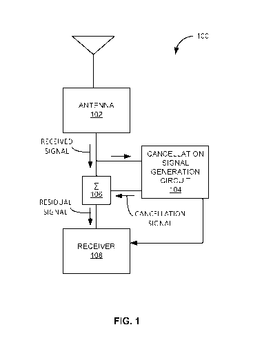
signals spread through the spectral range, with the remaining spectral range
including weak
signals and background noise. Additionally, plots 315, 325, and 335 include
the quantization
noise included in the signals post some corresponding process. The
quantization noise from the
processes is shown in subsequent plots for ease of comparison, but would not
be included in the
various signals as it would appear in the transceiver 200.
[0055] Plot 305 shows the RF input signal as provided by the antenna 202, for
example. The plot shows the strong signals, the weak signals, and the
background noise. The
RF signal as shown in plot 305 may be provided as an input to the ADC 214 and
the summer
206.
[0056] Plot 315 shows the RF input signal and the quantization noise post
sampling by
the ADC 214, e.g., ADC QUANT'N NOISE. The quantization noise may be generated
by the
sampling process, as is known in the art, and is depicted as the light grey
broad spectrum signal.
Further, the noise floor, e.g., the level of the quantization noise, is above
the level of the weak
signals, which may cause the weak signals to be undetectable. As discussed
above, the weak
signals may be suppressed below the level of the noise floor due to the strong
signals either
saturating the ADC 214 and/or due to automatic gain control system lowing the
gain of the ADC
214. In effect, the fixed dynamic range of the ADC 214 may be consumed by the
strong signals
dominating the RF input signal. As such, if the transceiver 200 were to
attempt to use the digital
sample as a final signal to provide to the application processor 224, only the
strong signals may
be usable, rendering a majority of the RF input signal unusable.
[0057] Plot 325 shows the RF input signal and the quantization noise injected
by the
DAC 218 post digital-to-analog conversion by the DAC 218. The quantization
noise injected by
the DAC 218 is labeled DAC QUANT'N NOISE, and may be present in the analog
stream from
the DAC 218 to the receiver 208, for example. The lighter grey is the ADC
QUANT'N NOISE,
which is shown in plot 325 for comparison purposes only and may not be present
in the analog
19
CA 02997183 2018-03-01
WO 2017/041034 PCT/US2016/050261
stream in the transceiver 200. The DAC QUANT'N NOISE may be lower than the ADC
QUANT'N NOISE due to the DAC 218 being based on a higher number of bits, which
may
generate less quantization noise. However, even though it may be lower, the
DAC QUANT'N
NOISE may dominate and obscure many of the weak signals in the RF input
signal.
[0058] Plot 335 shows the RF input signal and the ADC and DAC quantization
noise,
and the system noise floor after the digital residual signal has been
processed by the signal
processor 222. The plot 335 may be the digital representation of the RF input
signal after the
injected quantization noise, e.g., the DAC QUANT'N NOISE, has been subtracted
from the
digital residual signal. Although the ADC and DAC quantization noises are
shown in plot 335,
their depiction is for purposes of illustration and would not be in the actual
signal provided by
the signal processor 222. The system noise floor may be the lower noise of the
transceiver 200,
but may be low enough so that all, or almost all, weak signals are usable by
downstream
components, such as the application processor 224. The strong signals included
in the plot 335
may also be the original strong signals as sampled by the ADC 214, which may
have been added
into the digital residual signal by the signal processor 222.
[0059] As illustrated by plot 335, the transceiver 200 may be characterized as
a high-
bandwidth, high dynamic range radio. The high dynamic range shown by the large
signal
strength difference between the weakest of the weak signals and the strong
signals.
[0060] Figure 4 is an example method 400 of a wide-band, high dynamic range
direct-
sample transceiver in accordance with an embodiment of the present disclosure.
The method
400 may illustrate an example operation of the transceiver 200.
[0061] The method 400 may begin at process block 402, which includes receiving
the
input signal by a wide-band antenna, such as the antenna 202. The input signal
may be an RF
input signal that spans at least two gigahertz of frequency, and include weak
signals and at least
one strong signal. The strong signal is at least 50 dB stronger than the weak
signals, for
example.
CA 02997183 2018-03-01
WO 2017/041034 PCT/US2016/050261
[0062] The process block 402 may be followed by the process block 404, which
may
include oversampling an input signal to provide a digital sample signal of at
least the strong
signal. The oversampling may be performed by an ADC, such as the ADC 214,
which may be
an 8-bit ADC sampling at a rate of 5 GHz, for example. The digital sample may
only include the
strong signal due to the strong signal causing the weak signals to be
suppressed below the noise
floor of the ADC, which may be due to the relative strength of the strong
signal to the weak
signals. The relative strength of the signals may affect the dynamic range of
the ADC.
[0063] The process block 404 may be followed by the process block 406, which
includes generating a digital cancellation signal of the strong signal based
on the digital sample
signal. The digital cancellation signal may be formed by a digital signal
processor, such as the
signal processor 216. Additionally, the number of bits used to define the
digital cancellation
signal may be greater than generated by the ADC. For example, the number of
bits to define the
digital cancellation signal may be 13. Further, the digital cancellation
signal may be the
complement of the digital sample, e.g., a negative of, so that the strong
signal may be removed
or reduced when the analog cancellation signal is added to the RF input
signal.
[0064] The process block 406 may be followed by the process block 408, which
includes generating an analog cancellation signal based on the digital
cancellation signal. The
analog cancellation signal, which may be generated by a DAC, such as the DAC
218, may
provide a more precise estimate of the strong signal than the digital sample
signal provides. The
DAC may be a 13-bit DAC, in some embodiments.
[0065] The process block 408 may be followed by the process block 410, which
includes summing the analog cancellation signal and the input signal to
provide a residual signal.
The summation may be performed by the adder 212, for example. The residual
signal may
include the weak signals and a suppressed strong signal. In some embodiments,
the strong signal
may be absent in the residual signal.
21
CA 02997183 2018-03-01
WO 2017/041034 PCT/US2016/050261
[0066] The process block 410 may be followed by the process block 412, which
includes generating a digital residual signal based on the residual signal.
The digital residual
signal may be formed by an ADC, such as the ADC 220. The residual signal may
have
quantization noise due to the conversion of the analog cancellation signal,
which may be injected
into the analog cancellation signal by the DAC 218.
[0067] The process block 412 may be followed by the process block 414, which
includes removing the quantization noise from the digital residual signal. A
digital signal
processor, such as the signal processor 222, may estimate the quantization
noise based on apriori
knowledge of the strong signal, and then remove the quantization noise from
the digital residual
signal. Accordingly, removal of the quantization noise from the digital
residual signal may
uncover the weak signals, which may make them usable.
[0068] The process block 414 may be followed by the process block 416, which
includes inserting the strong signal into the digital residual signal to
provide a digital
representation of the input signal including the weak signals and the strong
signal. The signal
processor 222, for example, may insert the strong signal back into the digital
residual signal
because the strong signal may be a signal of interest.
[0069] The order in which some or all of the process blocks appear in the
method 400
should not be deemed limiting. Rather, one of ordinary skill in the art having
the benefit of the
present disclosure will understand that some of the process blocks may be
executed in a variety
of orders not illustrated, or even in parallel.
[0070] Figure 5 is an example computer readable storage medium 500 for
implementing a wide-band, high dynamic range direct-sample transceiver in
accordance with an
embodiment of the present disclosure. The computer readable storage medium
(CRM) 500 may
include instruction set 505 to implement the method 400, for example. CRM 500
may be
coupled to or incorporated into a computing system or machine and may be
performed by the
22
CA 02997183 2018-03-01
WO 2017/041034 PCT/US2016/050261
computing system/machine in order to implement an example wide-band, high
dynamic range
direct-sample transceiver.
[0071] The instruction set 505 may include instructions that may cause an
executing
computing system or machine to oversample an input signal to provide a digital
sample signal.
The input signal may be a wide-band RF signal having weak signals and a strong
signal, and the
digital sample signal is based on N-bit sampling. In some embodiments, N may
be 8 and the
input signal may be sampled at 5 GHz.
[0072] The instruction set 505 may further cause the machine to generate a
digital
cancellation signal of the strong signal based on the digital sample signal,
where the digital
cancellation signal is an M-bit signal, and M may be greater than N. In some
embodiments, M
may be 13. Further, the instruction set 505 may cause the computing system or
machine to
generate an analog cancellation signal based on the digital cancellation
signal, and sum the input
signal with the analog cancellation signal to generate a residual signal. The
residual signal may
be an analog signal including the weak signals and at least a reduced strong
signal. In some
embodiments, the strong signal may be removed from the residual signal.
[0073] The instruction set 505 may further cause the computing system or
machine to
sample the residual signal to generate a digital residual signal, where the
digital residual signal
includes quantization noise injected by the generation of the analog
cancellation signal, and
estimate the quantization noise based on knowledge of the strong signal in the
input signal. The
quantization noise may further be subtracted from the digital residual signal
to recover the weak
signals in the digital residual signal, and the strong signal may be inserted
into the digital
residual signal to provide a digital representation of the input signal.
[0074] The processes explained above are described in terms of computer
software and
hardware. The techniques described may constitute machine-executable
instructions embodied
within a tangible or non-transitory machine (e.g., computer) readable storage
medium, that when
executed by a machine will cause the machine to perform the operations
described.
23
CA 02997183 2018-03-01
WO 2017/041034 PCT/US2016/050261
Additionally, the processes may be embodied within hardware, such as an
application specific
integrated circuit ("AS-IC") or programmable firmware such as a field
programmable gate array
("ASIC"), or otherwise.
[0075] A tangible machine-readable storage medium includes any mechanism that
provides (i.e., stores) information in a non-transitory form accessible by a
machine (e.g., a
computer, network device, personal digital assistant, manufacturing tool, any
device with a set of
one or more processors, etc.). For example, a machine-readable storage medium
includes
recordable/non-recordable media (e.g., read only memory (ROM), random access
memory
(RAM), magnetic disk storage media, optical storage media, flash memory
devices, etc.).
[0076] The above description of illustrated embodiments of the invention,
including
what is described in the Abstract, is not intended to be exhaustive or to
limit the invention to the
precise forms disclosed. While specific embodiments of, and examples for, the
invention are
described herein for illustrative purposes, various modifications are possible
within the scope of
the invention, as those skilled in the relevant art will recognize.
[0077] These modifications can be made to the invention in light of the above
detailed
description. The terms used in the following claims should not be construed to
limit the
invention to the specific embodiments disclosed in the specification. Rather,
the scope of the
invention is to be determined entirely by the following claims, which are to
be construed in
accordance with established doctrines of claim interpretation.
24