Note: Descriptions are shown in the official language in which they were submitted.
CA 02998688 2018-03-14
WO 2017/051019 PCT/EP2016/072774
Title: Polymer coatings and methods for depositing polymer coatings.
Description of Invention
The present invention relates to polymer coatings and methods for depositing
polymer coatings and, in particular, to polymer coatings for improving the
corrosion resistance of substrates, e.g. electronic devices or component parts
thereof. In some embodiments, the invention may relate to an electronic device
or
one or more components thereof-such as a printed circuit board (PCB) - having
a
polymer coating thereon.
The electronics industry is a fast growing industry. Electronic devices such
as
smartphones, mobile phones, e-readers, tablets, computers, earphones,
headphones, speakers, e.g. portable speakers, are used all around the world on
a
daily basis.
The primary reason for failure of such electronic devices is damage by fluid
ingress
or ingress of humidity. Humidity condensates inside the device, and the
minerals
and salts therein generate corrosion spots, which can cause short circuiting
of
electrical connections. This short circuiting can lead to damage beyond repair
of the
device.
Upon exposure to water (or other liquids), many manufacturers advise their
customers to dry the product as soon as possible. However, some devices have
complex designs such that even after up to 48 hours of drying, water /
condensation can remain in the device. Thus, many devices are damaged beyond
repair either upon immediate exposure to water or during the drying process
due
to prolonged water exposure.
The most severe damage is observed when the device is powered on during water
ingression. Water on a powered electronic circuit that has not had any
protective
coating applied thereon can result in almost instant corrosion and consequent
short
circuiting of the electronics. This is because the minerals and salts
dissolved in
water act as electrical conductors.
CA 02998688 2018-03-14
WO 2017/051019 2 PCT/EP2016/072774
Embodiments of the present invention seek to provide improved methods for
depositing polymer coatings onto surfaces of substrates (such as electronic
devices
or component parts thereof) which methods have the effect of improving the
water
resistance of the deposited coating. In some embodiments, the invention seeks
to
provide a polymer coating which, when applied on a substrate, is able to
prevent
(or at least substantially prevent) water ingress through the coating to the
substrate, especially in cases when the component or device including the
substrate is powered on whilst exposed to water.
In one aspect of the invention we provide a method for protecting a substrate
from
corrosion, which method comprises in sequence:
a first step including plasma polymerization of a precursor monomer and
deposition of the resultant polymer onto at least one surface of a substrate;
a second step including exposing the polymer to an inert gas in the
presence of a plasma without further deposition of polymer onto the or each
surface of the substrate;
a third step including plasma polymerization of the precursor monomer used
in the first step and deposition of the resultant polymer onto the polymer
deposited
in the first step so as to increase the thickness of the polymer; and
optionally, a fourth step including exposing the polymer to an inert gas in
the presence of a plasma without further deposition of polymer onto the or
each
surface of the substrate.
The inert gas used in the optional fourth step may be the same as or different
from
the inert gas used in the second step.
The applicant has discovered that the step(s) of exposing the polymer to an
inert
gas in the presence of a plasma without further deposition of polymer
increases the
density of the polymer coating and / or changes the orientation of functional
groups on at least the surface of the polymer, thereby leading to improved
resistance to water through the polymer coating. For instance, the step(s) of
exposing the polymer to an inert gas in the presence of a plasma without
further
deposition of polymer can promote further crosslinking of at least the surface
of
the polymer, which has the effect of increasing the number of barriers through
which water must diffuse to reach the underlying substrate.
CA 02998688 2018-03-14
WO 2017/051019 3 PCT/EP2016/072774
In other words, exposing the polymer to an inert gas has the effect of
modifying
the surface of the polymer coating (without destroying the polymer coating) to
improve its resistance to water. Exposing the polymer to a reactive gas, such
as
H2 or 02, could at least partially destroy the polymer which could lead to a
reduction in its resistance to water.
The method may include repeating the third and fourth steps at least once
more,
so that the sequence is essentially first step : second step : first step :
second step
: first step : second step.
The method may include repeating the third and fourth steps up to about ninety
nine times, e.g. up to about forty nine times, e.g. up to about nineteen
times, e.g.
up to about nine times, such as up to about four times. For instance, in a
case
where the third and fourth steps are repeated ninety nine times the total
sequence
is essentially (first step : second step) x 100.
By repeating the steps the thickness of the polymer coating can be increased,
whilst at the same time providing discrete regions of the polymer with
increased
density. For instance, the first step may be carried out to deposit a polymer
coating followed by carrying out the second step. The second step does not add
to
the polymer coating but instead increases its density. The first step may then
be
carried out again so as to increase the thickness of the polymer coating,
followed
by a further second step to increase the density of the newly deposited
polymer
coating. By successively carrying out the first and second steps the resultant
polymer coating has increased numbers of barriers through which water must
diffuse. Thus, a polymer coating deposited by this method is more resistant to
water when compared to polymer coatings having the same thickness, but
deposited using conventional methods such as those including a single coating
step.
It goes without saying that the resultant coating consists of a polymer formed
from
a single monomer species, albeit with discrete regions of increased density.
This
'ingle layer" differs from the "multi-layer" polymer coatings found in the
prior art
which include two or more discrete layers of polymer, whereby at least two of
the
discrete layers are formed from different monomer species. The polymer coating
of the present invention is formed from a single monomer species.
CA 02998688 2018-03-14
4
WO 2017/051019 PCT/EP2016/072774
The method may involve repeating the steps until the polymer coating has a
total
thickness of from approximately 200 nm to approximately 10000 nm, e.g.
approximately 400 nm to approximately 8000 nm, such as approximately 5000 nm
or approximately 2500 nm or approximately 2000 nm or approximately 1500 nm
or approximately 1000 nm.
Each step including plasma polymerization of the precursor monomer may include
depositing polymer having a thickness from approximately 10 nm to
approximately
500 nm, e.g. from approximately 50 nm to approximately 200 nm, such as
approximately 100 nm. In some embodiments, each step including plasma
polymerization of the precursor monomer may include depositing polymer having
a
thickness from approximately 25 nm to approximately 200 nm, such as
approximately 50 nm.
Each step including plasma polymerization of a precursor monomer may be
carried
out for a duration that is greater than or equal to the duration of the
step(s)
including exposing the polymer to an inert gas in the presence of the plasma
without further deposition of polymer.
The duration of the step(s) including exposing the polymer to an inert gas in
the
presence of the plasma without further deposition of polymer may be from about
10 seconds to about 20 minutes, e.g. from about 1 minute to about 10 minutes.
In some embodiments, the duration of the step(s) including exposing the
polymer
to an inert gas in the presence of the plasma without further deposition of
polymer
may be from about 10 seconds to about 1 minute.
The power of the plasma in the step(s) including exposing the polymer to an
inert
gas in the presence of the plasma without further deposition of polymer may be
equal to or lower than the power of the plasma in each step including plasma
polymerization of a precursor monomer. Alternatively, the power of the plasma
in
the step(s) including exposing the polymer to an inert gas in the presence of
the
plasma without further deposition of polymer may be higher than the power of
the
plasma in each step including plasma polymerization of a precursor monomer,
e.g.
up to 200% of the power of the plasma in each step including plasma
polymerization of a precursor monomer.
CA 02998688 2018-03-14
WO 2017/051019 5 PCT/EP2016/072774
The power of the plasma in each step including plasma polymerization of a
precursor monomer may be from approximately 20 Watts to approximately 750
Watts, e.g. approximately 50 Watts to approximately 250 Watts.
The method may include continuous wave or pulsed wave plasma deposition.
The power of the plasma in the step(s) including exposing the polymer to an
inert
gas in the presence of the plasma without further deposition of polymer may be
from approximately 10 Watts to approximately 750 Watts, e.g. approximately 50
Watts to approximately 150 Watts.
The applicant has discovered that by carrying out the step(s) including
exposing
the polymer to an inert gas in the presence of the plasma without further
deposition of polymer for a shorter duration than each step including plasma
polymerization of a precursor monomer the resultant polymer coating has
increased resistance to water. Without being bound to any particular theory,
it is
believed that by carrying out the step(s) including exposing the polymer to an
inert
gas in the presence of the plasma without further deposition of polymer for
relatively short periods the degree of crosslinking of the polymer coating is
maximized without causing degradation of the polymer coating. In other words,
the physical properties of the polymer are changed during said step(s) by
exposure
to the inert gas in the presence of a plasma.
The inert gas may comprise any one of Ar, N2, He, Ne, Kr, Xe, or a mixture
thereof.
The precursor monomer may be:
= acrylate;
= methacrylate; or
= organosilane.
The precursor monomer may comprise a compound having the general formula (I):
CnF2n-F1CmX2mCR1Y-OCO-C(R2)=CH2 (I)
wherein:
n is 2 to 8;
m is 0 to 9;
X and Y are independently H, F, Cl, Br or I;
R1 is H or alkyl, e.g.-CH3, or a substituted alkyl; and
CA 02998688 2018-03-14
WO 2017/051019 6 PCT/EP2016/072774
R2 is H or alkyl, e.g.-CH3, or a substituted alkyl.
In some embodiments the monomer is 1H, 1H, 2H, 2H-perfluorodecyl acrylate.
The precursor monomer may comprise a compound having the general formula
(II):
R3-Z-R4 (II)
wherein:
Z is 0 or NH;
R3 and R4 are each independently-Si(R5)(R6)R7; and
R5, R6, R7 are each independently H, an alkyl group of up to 10 carbon
atoms or an alkenyl group of up to 10 carbon atoms, wherein, in each of R3
and R4, at least two of R5, R6 or R7 is an alkyl group; and
the total number of carbon atoms in the precursor monomer is not more
than 20.
In embodiments R5, R6 and R7 are all alkyl groups. The alkyl groups may be
straight or branched-chain. The alkyl groups may be methyl or ethyl groups.
In some embodiments the precursor monomer is hexamethyldisiloxane (HMDSO).
In embodiments R5 and R6 may be alkyl groups and R7 may be an alkenyl group.
The alkyl groups may be straight or branched-chain. The alkyl groups may be
methyl or ethyl groups. The alkenyl group may be vinyl.
In some embodiments the precursor monomer is 1,3-divinyltetramethyldisiloxane.
Advantages of using organosilane precursor monomers having an alkenyl group
over organosilane precursor monomers without an alkenyl group are as follows.
The presence of one or more C=C in the alkenyl group means that this category
of
precursor monomer is more reactive than, for example, HMDSO. As such, 1,3-
divinyltetramethyldisiloxane, for example, requires less energy to initiate
polymerisation than HMDSO. Therefore, precursor monomers having alkenyl
groups may not require reactive carrier gasses, such as 02, because such
monomers can readily polymerise in the plasma without. Due to the increased
reactivity such monomers may also exhibit high rates of deposition when
compared
to organosilane precursor monomers without an alkenyl group. Advantageously,
CA 02998688 2018-03-14
7
WO 2017/051019 PCT/EP2016/072774
higher deposition rates lead to shorter processing times and higher throughput
for
users. The inventors have also determined that the presence of the alkenyl
group
results in a polymer coating having a denser crosslinked structure when
compared
to organosilane precursor monomers without an alkenyl group.
Denser
crosslinking has an effect of improving the polymer coatings resistance to
water
and other liquids.
The precursor monomer may comprise a cyclic compound having the general
formula (III):
-[Si(CH3)q(H)2_q-Z-b- (III)
wherein:
p is 2 to 10;
q is 0 to 2;
Z is 0 or NH; and
the total number of carbon atoms in the precursor monomer is not more
than 20.
The precursor monomer may be one in which p is 3, or p is 4, or p is 5, or p
is 6.
In embodiments the precursor monomer is hexamethylcyclotrisilazane.
The precursor monomer may comprise a compound having the general formula
(IV):
CH2 = C(R8)-si(R9)(R10)-R11 (IV)
wherein:
R8 is H or an alkyl group, e.g.-CH3; and
R9, R1 and R11 are each independently H, an alkyl group of up to 10 carbon
atoms or an alkoxy groupR1 2 ) , wherein R12 is preferably -CtH2t-F1, wherein
t is 1
to 10.
The precursor monomer may comprise a compound having the general formula
(V):
R13_si(R14)(R15)-R16 (V)
wherein:
R13 is H or an alkyl group, e.g.-CH3;
K-14,
R15 and R16 are each independently H, an alkyl group of up to 10 carbon
atoms or an alkoxy groupR1 2 ) wherein R12 is preferably -CtH2t-F1, wherein t
is 1
to 10.
CA 02998688 2018-03-14
WO 2017/051019 8 PCT/EP2016/072774
The alkoxy groups may be straight, branched or cyclic. In some embodiments the
alkoxy groups are methoxy or ethoxy groups.
The precursor monomer may comprise a compound having the general formula
(VI):
CH2=C(R17)C(0)-0-(CH2)r-Si(R18)(R19)-R20 (VI)
wherein:
r is from 0 to 10;
R17 is H or an alkyl group, e.g.-CH3;
K R19
and R2 are each independently H, an alkyl group of up to 10 carbon
atoms or an alkoxy group (R12-u r.,N
)
, wherein R12 is preferably -CtH2t+1, wherein t is 1
to 10.
The precursor monomer may be one in which r is 2 and wherein each of R18, R19
and R2 are an alkoxy group, e.g. methoxy. In some embodiments the precursor
monomer is 3-(trimethoxysilyl)propyl acrylate.
The alkoxy groups may be straight, branched or cyclic. In some embodiments the
alkoxy groups are methoxy or ethoxy groups.
In a second aspect of the invention we provide a method for protecting an
electronic device from corrosion, which method comprises:
a. providing an electronic device including a printed circuit board having
electronic components applied thereto;
b. plasma polymerization of a first precursor monomer and deposition
of the resultant polymer onto at least one surface of the printed
circuit board, wherein the first precursor monomer is an alkane,
alkene, alkyne or a mixture thereof; and
c. plasma polymerization of a second precursor monomer and
deposition of the resultant polymer onto the polymer formed in step
b., wherein the second precursor monomer is an acrylate,
methacrylate, organosilane or a mixture thereof.
The alkane, alkene or alkyne may be substituted, e.g. with one or more
heteroatom(s).
CA 02998688 2018-03-14
WO 2017/051019 9 PCT/EP2016/072774
The first precursor monomer may comprise a linear or branched alkane having
the
general formula (VII):
C,X2u+2 (VII)
wherein:
u is from 1 to 20, preferably from 1 to 10, even more preferably from 2 to
5; and
X is H, F, Cl, Br or I.
The first precursor monomer may comprise a linear or branched alkene having
the
general formula (VIII):
CvX2v (VIII)
wherein:
v is from 2 to 20, preferably from 2 to 10;
X is H, F, Cl, Br or I; and
the first precursor monomer may contain from 1 to 10 carbon-carbon
double bonds (C=C).
The first precursor monomer may be ethylene.
The first precursor monomer may comprise a linear or branched alkyne having
the
general formula (IX):
CwZ2w-2 (IX)
wherein:
w is from 2 to 20, preferably from 2 to 10;
Xis H, F, Cl, Br or I; and
the first precursor monomer may contain from 1 to 10 carbon-carbon triple
bonds (CEC), preferably from 1 to 2 carbon-carbon triple bonds.
The second precursor monomer may comprise a compound having the general
formula (I), (II), (III), (IV), (V) or (VI).
The polymer coating may have a total thickness of approximately 200 nm to
approximately 10000 nm, e.g. approximately 400 nm to approximately 8000 nm,
such as approximately 5000 nm or approximately 2500 nm or approximately 2000
nm or approximately 1500 nm or approximately 1000 nm. By total thickness, we
mean the combined thickness of polymer formed from the first precursor monomer
and polymer formed from the second precursor monomer.
CA 02998688 2018-03-14
WO 2017/051019 10 PCT/EP2016/072774
The polymer coating formed from the second precursor monomer may have a
thickness of approximately 10 nm to approximately 3000 nm, e.g. approximately
20 nm to approximately 1000 nm, e.g. approximately 50 nm to approximately 500
nm or approximately 250 nm.
The polymer coating formed from the first precursor monomer may have a
thickness of approximately 50 nm to approximately 9000 nm, e.g. approximately
100 nm to approximately 8000 nm, e.g. approximately 250 nm to approximately
5000 nm, e.g. approximately 500 nm to approximately 2500 nm, such as
approximately 2000 nm or approximately 1500 nm or approximately 1000 nm or
approximately 750 nm.
In a further aspect of the invention we provide a method for protecting a
substrate
from corrosion, which method comprises:
a first step including plasma polymerization of a precursor monomer and
deposition of the resultant polymer onto at least one surface of a substrate;
and
subsequently, a second step including exposing the polymer to a gas in the
presence of a plasma without further deposition of polymer onto the or each
surface of the substrate.
In a further aspect of the invention we provide a method for protecting a
substrate
from corrosion, which method comprises:
a. plasma polymerization of a first precursor monomer and deposition
of the resultant polymer onto at least one surface of a substrate,
wherein the first precursor monomer is an alkane, alkene, alkyne or
a mixture thereof; and
b. plasma polymerization of a second precursor monomer and
deposition of the resultant polymer onto the polymer formed in step
a., wherein the second precursor monomer is an acrylate,
methacrylate, organosilane or a mixture thereof.
The following features may apply to either aspect of the present invention.
An outgassing and/or pre-treatment step may be carried out prior to plasma
deposition of polymer.
CA 02998688 2018-03-14
WO 2017/051019 11 PCT/EP2016/072774
Outgassing removes not only contaminants and moisture from a surface of a
substrate, but also contaminants and moisture from internal surfaces, i.e.
surfaces
that are not directly exposed to the atmosphere but can be accessed via
openings
and channels. Outgassing of the substrates in the plasma chamber prior to
conducting the method allows for an improved penetration of the plasma into
the
substrate, resulting in an improved coating in terms of thickness and
performance,
in this case corrosion protection.
Pre-treatment may involve carrying out an activation and/or cleaning and/or
etching step.
The pre-treatment step may be performed using an inert gas (e.g. He or Ar) or
a
reactive gas (e.g. 02) or a combination of both.
In embodiments, the precursor monomer may be transported to a plasma chamber
by a carrier gas. A carrier gas is typically required when the precursor
monomer
does not easily vaporise. The carrier gas may be an inert gas which serves
solely to
transport the precursor monomer. Alternatively, the carrier gas may be a
reactive
gas which serves both to transport the precursor monomer and contribute to the
polymerisation reaction. The carrier gas may contribute to the polymerisation
reaction by striking the plasma to ignite the plasma, or by influencing the
polymerization reaction to realize coatings with a better performance.
Use of a carrier gas to transport precursor monomers is known in the art and
need
not be discussed further.
The invention may relate to a polymer coating formed according to a method of
any previous aspect.
The invention may also relate to a substrate (such as an electronic device or
component part thereof) having a polymer coating formed according to a method
of any previous aspect.
Embodiments of the invention will now be described, by way of example only,
with
reference to the accompanying figures.
Figures 1A and 1B show schematics of an electrical shortcut test;
CA 02998688 2018-03-14
WO 2017/051019 12 PCT/EP2016/072774
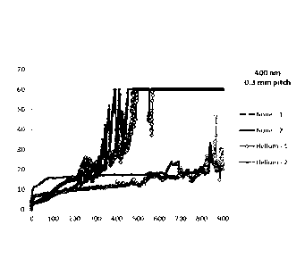
Figure 2 shows a graph comparing (i) PCBs coated with a polymer having a
thickness of 400 nm deposited using a conventional method (None); and (ii)
PCBs coated with the same polymer as (i) having a thickness of 400 nm
deposited using a method according to the invention (Helium);
Figures 3A to 3C show graphs comparing (i) PCBs coated with a polymer
having a thickness of 2000 nm deposited using a conventional method (No
sequence); and (ii) PCBs coated with the same polymer as (i) having a
thickness of 2000 nm deposited using a method according to the invention
(Stacked);
Figures 4A to 4C show graphs comparing (i) PCBs coated with a polymer
having a thickness of 5000 nm deposited using a conventional method (No
sequence); and (ii) PCBs coated with the same polymer as (i) having a
thickness of 5000 nm deposited using a method according to the invention
(Stacked);
Figures 5A to 5C show graphs comparing (i) PCBs coated with a polymer
having a thickness of 8000 nm deposited using a conventional method (No
sequence); and (ii) PCBs coated with the same polymer as (i) having a
thickness of 8000 nm deposited using a method according to the invention
(Stacked);
Figure 6 shows a graph comparing (i) PCBs coated with a single polymer
having a thickness of 1000 nm (no supporting layer); and (ii) PCBs coated
with first and second polymer layers having a total thickness of 1000 nm
(supporting layer).
To test the performance of coatings an electrical shortcut test was carried
out,
which involves submersing a substrate-in this case a printed circuit board
(PCB)-in
water whilst powered.
Figures 1A and 1B show the schematic set-up of the electrical shortcut test.
Wires
105 and 106 are connected to a PCB 104. The opposite end of wire 105 is
connected to a power supply 101 and the opposite end of wire 106 is connected
to
a multimeter 102, which measures currents in the pA and mA range. Multimeter
CA 02998688 2018-03-14
WO 2017/051019 13 PCT/EP2016/072774
102 and power supply 101 are connected through a wire 107. After the circuit
has
been prepared, the PCB 104 is placed horizontally in water 103. Bottled water
is
preferred to ensure stability for repeat testing. Alternatively, tap water may
be
used. The water may have a temperature of from 20 C to 25 C. The PCB may be
submersed to a depth of 5 mm.
The PCB 104 itself may consist of a pair of comb patterns 108, 109. The
patterns
108, 109 may be formed from spaced-apart copper tracks 111. The distance
between the copper tracks 111 is the so-called"pitclf 110.
Typically, the pitch 110 varies between 0.3 mm and 5.0 mm, which are normal
distances used on electronic components. Typically, the copper tracks 111 are
between 0.5 mm and 2.0 mm wide.
To start the test, the power supply 101 is turned on at a set value, which
remains
constant over the whole test duration. Alternatively, a current limitation may
be
set, which reduces the applied power when a maximal current, e.g. of 60 mA or
180 mA, is reached, to protect the circuit, power supply and multimeter.
The set power value may be chosen as a function of the average, typical,
minimal
or maximal power that is generated on the electronic device when used. A
typical
average value for a battery connection of a smartphone is 4.7 V. A typical
average
value for a camera flash, a charge portal or a touchscreen device may be up to
24
V or higher.
Once the power is turned on via the power supply 101, the current that flows
from
the copper tracks 111 of one comb structure 108 to the copper tracks 111 of
the
other comb structure 109 is measured by multimeter 102 and is logged. This
current is so-called "shortcut current', or "short circuiting current', as it
means a
current bridge is formed between the two comb patterns 108 and 109, which are
separated from each other. In air, the resistance between the copper tracks
111 of
comb structures 108 and 109 is very high, so no current is measured.
Damage in the form of corrosion and short circuiting is measured by an
increase in
current for a given applied voltage, which implies a decrease of resistance
over the
copper tracks 111 of the comb patterns 108 and 109.
CA 02998688 2018-03-14
WO 2017/051019 14 PCT/EP2016/072774
The electrical shortcut test duration is typically up to 20 minutes, such as
up to 15
minutes.
Comparison of"no post treatmenrand"post treatment'
A coating was deposited onto a PCB having a pitch of 0.3 mm according to a
conventional low pressure polymerisation method (Table 1). The polymer coating
has a thickness of 400 nm. The precursor monomer used was an acrylate, namely
1H,1H,2H,2H-Perfluorodecyl acrylate.
Parameter Value
Plasma Chamber
Dimensions 700 x 700 x 1000 mm
Temperature wall 30-60 C
Electrodes RF/ground
Pre-treatment
Gas Argon
Flow 300-500 sccm
Power 300- 600 W
Frequency 13.56 MHz
Frequency mode Cw
Time 5 minutes
Coating
Monomer 1H,1H,2H,2H-Perfluorodecyl
acrylate
Flow 25-50 sccm
Additional gas -
Flow ( /0 of monomer flow) -
Base pressure 10-30 mTorr
Work pressure 20-75 mTorr
Power 40-150 W
Frequency 13.56 MHz
Frequency mode cw
Time 20 minutes
Table 1: Conventional method (no post treatment)
CA 02998688 2018-03-14
WO 2017/051019 15 PCT/EP2016/072774
A coating was deposited onto a PCB having a pitch of 0.3 mm according to a low
pressure polymerisation method according to the invention (Table 2). The
polymer
coating had a thickness of 400 nm. The same precursor monomer to the
conventional method was used, namely 1H,1H,2H,2H-Perfluorodecyl acrylate. The
method according to the invention involved a second step subsequent to the
polymerisation step, in which the polymer coating was exposed to Helium in the
presence of a plasma (post treatment). The second step did not involve further
deposition of polymer onto the PCB, but instead promoted a change in the
physical
properties of at least the surface of the polymer coating. As mentioned
previously,
the applicant has discovered that the density of the polymer coating on at
least a
surface thereof can be increased (without damaging the polymer coating) by
exposing the polymer coating to an inert gas in the presence of a plasma.
Parameter Value
Plasma Chamber
Dimensions 700 x 700 x 1000 mm
Temperature wall 30-60 C
Electrodes RF/g round
Pre-treatment
Gas Argon
Flow 300- 500 sccm
Power 300- 600 W
Frequency 13.56 MHz
Frequency mode cw
Time 5 minutes
Coating
Monomer 1H,1H,2H,2H-Perfluorodecyl
acrylate
Flow 25-50 sccm
Additional gas -
Flow (% of monomer flow) -
Base pressure 10-30 mTorr
Work pressure 20-75 mTorr
Power 40-150W
Frequency 13.56 MHz
Frequency mode cw
CA 02998688 2018-03-14
W02017/051019 16 PCT/EP2016/072774
Time 20 minutes
Post-treatment
Gas Helium
Flow 50- 200 sccm
Power 50- 150 W
Frequency 13.56 MHz
Frequency mode cw
Time 5-10 minutes
Table 2: Method according to the invention (post treatment)
An electrical shortcut test (as described above) was conducted on each coated
PCB
(i.e. no post treatment and post treatment). The electrical shortcut test was
carried out on two PCBs that had been subjected to the method of Table 1 (no
post
treatment) and two PCBs that had been subjected to the method of Table 2 (post
treatment).
Figure 2 is a plot of the electrical shortcut test data. The current (mA) is
shown
along the y-axis and time (seconds) is shown along the x-axis.
The measured shortcut current after 900 seconds of water submersion has been
recorded in Table 3 for the conventional method (no post treatment) and the
inventive method (post treatment). Table 3 shows the average shortcut current
measured from the two tests.
The degree of protection of the PCB afforded by the polymer coating is
inversely
proportional to the measured current. Thus, the lower the current the higher
the
degree of protection afforded by the polymer coating.
Post-treatment Current (mA) after
900 seconds
No 58.3
Yes 20.1
Table 3: Shortcut currents for no post-treatment vs post-treatment; 0.3 mm
pitch;
400 nm polymer coating
CA 02998688 2018-03-14
WO 2017/051019 17 PCT/EP2016/072774
It is clear from Table 3 and Figure 2 that after 900 seconds submersion, the
helium
post-treatment results are significantly better than without post-treatment.
The
effect of the post-treatment is significant even for such a narrow pitch - 0.3
mm.
After 900 seconds submersion, the shortcut value for a 0.3 mm pitch PCB with
post-treatment and a 400 nm thick coating is 65.5 % lower than the shortcut
value
for a 0.3 mm pitch PCB without post-treatment.
Comparison of"no post treatmenrand"repeated polymerisation / post treatment'
1. Polymer coating having a thickness of 2 pm
2 pm polymer coatings were deposited onto PCBs having pitches of 0.3 mm, 1.1
mm and 5 mm according to the conventional low pressure polymerisation method
(Table 1), with the exception that the coating time was increased from 20
minutes
to 100 minutes. The reason for increasing the coating time is that it takes
(under
the conditions in Table 1) approximately 1 minute to deposit a coating having
a
thickness of approximately 20 nm. Thus, it follows that it will take
approximately
100 minutes to deposit a coating having a thickness of approximately 2 pm. The
precursor monomer used was an acrylate, namely 1H,1H,2H,2H-Perfluorodecyl
acrylate.
2 pm polymer coatings were deposited onto PCBs having pitches of 0.3 mm, 1.1
mm and 5 mm according to a low pressure polymerisation method according to the
invention (Table 4). The same precursor monomer to the conventional method
was used, namely 1H,1H,2H,2H-Perfluorodecyl acrylate. The method according to
the invention involved a second step subsequent to the polymerisation step, in
which the polymer coating was exposed to Helium in the presence of a plasma
(post treatment). The method additionally involved repeating the
polymerisation
and post-treatment steps a further nine times. In other words, the sequence
was
(first step : second step) x 10.
Parameter Value
Plasma Chamber
Dimensions 700 x 700 x 1000 mm
CA 02998688 2018-03-14
WO 2017/051019 18 PCT/EP2016/072774
Temperature wall 30-60 C
Electrodes RF/ground
Pre-treatment
Gas Argon
Flow 300-500 sccm
Power 300-600W
Frequency 13.56 MHz
Frequency mode cw
Time 5 minutes
Coating
Monomer 1H,1H,2H,2H-Perfluorodecyl acrylate
Flow 25- 50 sccm
Additional gas
Flow (% of monomer flow)
Base pressure 10-30 mTorr
Work pressure 20-75 mTorr
Power 40- 150 W
Frequency 13.56 MHz
Frequency mode cw
Time 10 minutes
Post-treatment
Gas Helium
Flow 50- 200 sccm
Power 50- 150 W
Frequency 13.56 MHz
Frequency mode cw
Time 1-5 minutes
Table 4: Method according to the invention-repeated polymerisation / post
treatment
An electrical shortcut test was conducted on each coated PCB. The test was
carried
out twice for the PCBs having 0.3 mm and 1.1 mm pitches and once for the PCBs
having a 5.0 mm pitch.
CA 02998688 2018-03-14
WO 2017/051019 19 PCT/EP2016/072774
Figures 3A (0.3 mm pitch), 3B (1.1 mm pitch) and 3C (5.0 mm pitch) are plots
of
the electrical shortcut test data.
The measured shortcut currents after 60 seconds and 900 seconds of water
submersion have been recorded in Table 5 (0.3 mm pitch), Table 6 (1.1 mm
pitch)
and Table 7 (5.0 mm pitch) for the conventional method (no post treatment) and
the inventive method (which involved repeating polymerisation and post
treatment
steps). Tables 5 and 6 show the average shortcut current measured from the two
tests.
Table 5 to 7 and Figure 3A to 3C show that a higher degree of protection of
the
PCB by the polymer coating can be afforded by conducting repeated
polymerisation
and post treatment steps.
Post-treatment Current (mA) after 60 Current (mA) after 900
seconds seconds
No 3.3 11.9
Yes 0.21 0.39
Table 5: Shortcut currents for no post-treatment vs repeated polymerisation /
post
treatment; 0.3 mm pitch; 2 pm polymer coating
Post-treatment Current (mA) after 60 Current (mA) after
seconds 900 seconds
No 4.0 12.9
Yes 0.25 0.41
Table 6: Shortcut currents for no post-treatment vs repeated polymerisation /
post
treatment; 1.1 mm pitch; 2 pm polymer coating
Post-treatment Current (mA) after 60 Current (mA) after
seconds 900 seconds
No 1.1 12.2
Yes 0.35 0.57
CA 02998688 2018-03-14
WO 2017/051019 20 PCT/EP2016/072774
Table 7: Shortcut currents for no post-treatment vs repeated polymerisation /
post
treatment; 5.0 mm pitch; 2 pm polymer coating
It is clear from Tables 5 to 7 and Figures 3A to 3C that after 900 seconds
submersion, the repeated polymerisation / post treatment results are
significantly
better than without post treatment.
For example, after 60 seconds submersion, the shortcut value for a 0.3 mm
pitch
PCB with a 2 pm thick polymer coating deposited using repeated polymerisation
/
post treatment steps is 93.8 % lower than the shortcut value for a 0.3 mm
pitch
PCB with a 2 pm thick polymer coating deposited without post treatment.
For example, after 900 seconds submersion, the shortcut value of a 1.1 mm
pitch
PCB with a 2 pm thick polymer coating deposited using repeated polymerisation
/
post treatment steps is 96.8 % lower than the shortcut value of a 1.1 mm pitch
PCB with a 2 pm thick polymer coating deposited without post treatment.
2. Polymer coating having a thickness of 5 pm
5 pm polymer coatings were deposited onto PCBs having pitches of 0.3 mm, 1.1
mm and 5 mm according to the conventional low pressure polymerisation method
(Table 1), with the exception that the coating time was increased from 20
minutes
to 250 minutes to deposit the 5 pm coating. The precursor monomer used was an
acrylate, namely 1H,1H,2H,2H-Perfluorodecyl acrylate.
5 pm polymer coatings were deposited onto PCBs having pitches of 0.3 mm, 1.1
mm and 5 mm according to a low pressure polymerisation method according to the
invention (Table 4). The same precursor monomer to the conventional method
was used, namely 1H,1H,2H,2H-Perfluorodecyl acrylate. The method according to
the invention involved a second step subsequent to the polymerisation step, in
which the polymer coating was exposed to Helium in the presence of a plasma
(post treatment). The method additionally involved repeating the
polymerisation
and post-treatment steps a further twenty four times. In other words, the
sequence was (first step : second step) x 25.
An electrical shortcut test was conducted on each PCB.
CA 02998688 2018-03-14
WO 2017/051019 21 PCT/EP2016/072774
Figures 4A (0.3 mm pitch), 4B (1.1 mm pitch) and 4C (5.0 mm pitch) are plots
of
the electrical shortcut test data.
The measured shortcut currents after 60 seconds and 900 seconds of water
submersion have been recorded in Table 8 (0.3 mm pitch), Table 9 (1.1 mm
pitch)
and Table 10 (5.0 mm pitch) for the conventional method (no post treatment)
and
the inventive method (which involved repeating polymerisation and post
treatment
steps).
Post-treatment Current (mA) after 60 Current (mA) after
seconds 900 seconds
No 0.44 1.02
Yes 0.02 < 0.1 0.002 < 0.1
Table 8: Shortcut currents for no post-treatment vs repeated polymerisation /
post
treatment; 0.3 mm pitch; 5 pm polymer coating
Post-treatment Current (mA) after 60 Current (mA) after
seconds 900 seconds
No 0.79 3.57
Yes 0.01 < 0.1 0.03 < 0.1
Table 9: Shortcut currents for no post-treatment vs repeated polymerisation /
post
treatment; 1.1 mm pitch; 5 pm polymer coating
Post-treatment Current (mA) after 60 Current (mA) after
seconds 900 seconds
No 0.83 2.52
Yes 5.6E-09 < 0.1 2.02E-05 < 0.1
Table 10: Shortcut currents for no post-treatment vs repeated polymerisation /
post treatment; 5.0 mm pitch; 5 pm polymer coating
It is clear from Tables 8 to 10 and Figures 4A to 4C that after 900 seconds
submersion, the repeated polymerisation / post treatment results are
significantly
better than without post treatment.
CA 02998688 2018-03-14
WO 2017/051019 22 PCT/EP2016/072774
For example, after 60 seconds submersion, the shortcut value of a 0.3 mm pitch
PCB with a 5 pm thick polymer coating deposited using repeated polymerisation
/
post treatment steps is 95.9 % lower than the shortcut value of a 0.3 mm pitch
PCB with a 5 pm thick polymer coating deposited without post treatment.
For example, after 15 minutes submersion, the shortcut value of a 1.1 mm pitch
PCB with a 5 pm thick polymer coating deposited using repeated polymerisation
/
post treatment steps is 99.2 % lower than the shortcut value of a 1.1 mm pitch
PCB with a 5 pm thick polymer coating deposited without post treatment.
For the 3 measured pitches- 0.3 mm, 1.1 mm and 5.0 mm-the 5 pm thick polymer
coating deposited using repeated polymerisation / post treatment steps shows
shortcut current values much lower than the limit of visual corrosion (0.1
mA).
3. Polymer coating having a thickness of 8 pm
8 pm polymer coatings were deposited onto PCBs having pitches of 0.3 mm, 0.9
mm and 5 mm according to the conventional low pressure polymerisation method
(Table 1), with the exception that the coating time was increased from 20
minutes
to 400 minutes to deposit the 8 pm coating. The precursor monomer used was an
acrylate, namely 1H,1H,2H,2H-Perfluorodecyl acrylate.
8 pm polymer coatings were deposited onto PCBs having pitches of 0.3 mm, 0.9
mm and 5 mm according to a low pressure polymerisation method according to the
invention (Table 4). The same precursor monomer to the conventional method
was used, namely 1H,1H,2H,2H-Perfluorodecyl acrylate. The method according to
the invention involved a second step subsequent to the polymerisation step, in
which the polymer coating was exposed to Helium in the presence of a plasma
(post treatment). The method additionally involved repeating the
polymerisation
and post-treatment steps a further thirty nine times. In other words, the
sequence
went (first step : second step) x 40
An electrical shortcut test was conducted on each PCB.
Figures 5A (0.3 mm pitch), 5B (0.9 mm pitch) and 5C (5.0 mm pitch) are plots
of
the electrical shortcut test data.
CA 02998688 2018-03-14
WO 2017/051019 23
PCT/EP2016/072774
The measured shortcut currents after 60 seconds and 900 seconds of water
submersion have been recorded in Table 11 (0.3 mm pitch), Table 12 (0.9 mm
pitch) and Table 13 (5.0 mm pitch) for the conventional method (no post
treatment) and the inventive method (which involved repeating polymerisation
and
post treatment steps).
Post-treatment Current (mA) after 60 Current (mA) after
seconds 900 seconds
No 0.40 1.12
Yes 0.002 < 0.1 0.01 < 0.1
Table 11: Shortcut currents for no post-treatment vs repeated polymerisation /
post treatment; 0.3 mm pitch; 8 pm polymer coating
Post-treatment Current (mA) after 60 Current (mA) after
seconds 900 seconds
No 0.63 1.53
Yes 2.19E-06 < 0.1 1.39E-05 < 0.1
Table 12: Shortcut currents for no post-treatment vs repeated polymerisation /
post treatment; 0.9 mm pitch; 8 pm polymer coating
Post-treatment Current (mA) after 60 Current (mA) after
seconds 900 seconds
No 0.25 1.21
Yes 0.001 < 0.1 0.002 < 0.1
Table 13: Shortcut currents for no post-treatment vs repeated polymerisation /
post treatment; 5.0 mm pitch; 8 pm polymer coating
It is clear from Tables 11 to 13 and Figures 5A to 5C that after 900 seconds
submersion, the repeated polymerisation / post treatment results are
significantly
better than without post treatment.
For example, after 60 seconds submersion, the shortcut value of a 0.3 mm pitch
PCB with a 8 pm thick polymer coating deposited using repeated polymerisation
/
CA 02998688 2018-03-14
WO 2017/051019 24 PCT/EP2016/072774
post treatment steps is 99.5 % lower than the shortcut value of a 0.3 mm pitch
PCB with a 8 pm thick polymer coating deposited without post treatment.
For example, after 900 seconds submersion, the shortcut value of a 0.9 mm
pitch
PCB with a 8 pm thick polymer coating deposited using repeated polymerisation
/
post treatment steps is 99.9 % lower than the shortcut value of a 0.9 mm pitch
PCB with a 8 pm thick polymer coating deposited without post treatment.
For the 3 measured pitches- 0.3 mm, 0.9 mm and 5.0 mm-the 8 pm thick polymer
coating deposited using repeated polymerisation / post treatment steps shows
shortcut current values much lower than the limit of visual corrosion (0.1
mA).
Comparison of"no supporting layerand"supporting layer"
A polymer coating was deposited onto a PCB having a pitch size of 1.1 mm
according to the parameters and monomer listed in Table 14. The precursor
monomer used was a siloxane, namely Hexamethyldisiloxane. The polymer
coating had a thickness of 1000 nm and comprised only polyhexamethyldisiloxane
(no supporting layer).
Parameter Value
Plasma Chamber
Dimensions 500 x 400 x 250 mm
Temperature wall 30-60 C
Electrodes RF/ground
Pre-treatment
Gas Argon
Flow 10- 200 sccm
Power 50-300W
Frequency 13.56 MHz
Frequency mode cw
Time 1-5 minutes
Supporting layer None
Coating
Monomer Hexamethyldisiloxane
Flow 5-20 sccm
CA 02998688 2018-03-14
WO 2017/051019 25 PCT/EP2016/072774
Additional gas Oxygen (02)
Flow (% of monomer flow) 5-20 %
Base pressure 10-20 mTorr
Work pressure 20-50 mTorr
Power 100-300W
Frequency 13.56 MHz
Frequency mode cw
Table 14: Conventional method (no supporting layer)
A polymer coating was deposited onto a PCB having a pitch size of 1.1 mm
according to the parameters and monomers listed in Table 15. The polymer
coating comprised a first layer of a polymerised alkene, namely polyethylene,
and
a second layer of polymerised siloxane, namely polyhexamethyldisiloxane. The
first layer had a thickness of approximately 200 nm and the second layer had a
thickness of approximately 800 nm, resulting in a total polymer coating having
a
thickness of approximately 1000 nm.
Parameter Value
Plasma Chamber
Dimensions 500 x 400 x 250 mm
Temperature wall 30-60 C
Electrodes RF/ground
Pre-treatment
Gas Argon
Flow 10- 200 sccm
Power 50-300W
Frequency 13.56 MHz
Frequency mode cw
Time 1-5 minutes
Supporting layer
Monomer Ethylene
Flow 5-20 sccm
Power 100-300W
Frequency 13.56 MHz
Frequency mode cw
Coating
CA 02998688 2018-03-14
WO 2017/051019 26 PCT/EP2016/072774
Monomer Hexamethyldisiloxane
Flow 5-20 sccm
Additional gas Oxygen (02)
Flow (% of monomer flow) 5-20 %
Base pressure 10-20 mTorr
Work pressure 20-50 mTorr
Power 100-300W
Frequency 13.56 MHz
Frequency mode cw
Table 15: Method according to the invention (supporting layer)
An electrical shortcut test was conducted on each PCB. The electrical shortcut
test
was carried out on two PCBs that had been subjected to the method of Table 14
(no supporting layer) and two PCBs that had been subjected to the method of
Table 15 (supporting layer).
Figure 6 shows plots of the electrical shortcut test data.
The measured shortcut currents after 60 seconds and 900 seconds of water
submersion have been recorded in Table 16. Table 16 shows the average shortcut
current measured from the two tests.
Supporting layer Coating layer Current (mA) Current (mA)
after 60 seconds after 900 seconds
1000 nm 2.1 4.3
200 nm 800 nm 0.11 0.09 < 0.1
Table 16: Shortcut currents comparing no supporting layer and supporting
layer;
1.1 mm pitch; 1000 nm total polymer coating thickness
It is clear from Table 16 and Figure 6 that by providing a polyethylene
supporting
layer beneath the polyhexamethyldisiloxane coating the shortcut currents are
significantly lower than the shortcut currents for a single layer of
polyhexamethyldisiloxane, which indicates that the polymer coating with
supporting layer is more resistant to water than a conventional single layer
coating.
CA 02998688 2018-03-14
WO 2017/051019 27 PCT/EP2016/072774
For example, after 60 seconds submersion, the shortcut value of the 1.1 mm
pitch
PCB with a 200 nm polyethylene supporting layer and a 800 nm thick
polyhexamethyldisiloxane coating (total coating thickness of 1000 nm) is
around
0.1 mA, and is 94.7 % lower than the shortcut value of a 1.1 mm pitch PCB
without any supporting layer (coating thickness of 1000 nm).
For example, after 900 seconds submersion, the shortcut value of a 1.1 mm
pitch
PCB with a 200 nm polyethylene supporting layer and a 800 nm thick
polyhexamethyldisiloxane coating (total coating thickness of 1000 nm) is below
0.1
mA and is 97.8 % lower than the shortcut value of a 1.1 mm pitch PCB without
any
supporting layer (coating thickness of 1000 nm).
As used herein, the following terms have the following meanings:
"A", "an", and "the" as used herein refers to both singular and plural
referents
unless the context clearly dictates otherwise. By way of example, "a
compartment"
refers to one or more than one compartment.
"About" or"approximatelr as used herein referring to a measurable value such
as a
parameter, an amount, a temporal duration, and the like, is meant to encompass
variations of +/-20% or less, preferably +/-10% or less, more preferably +/-5%
or
less, even more preferably +/-1% or less, and still more preferably +/-0.1% or
less of and from the specified value, in so far such variations are
appropriate to
perform in the disclosed invention. However, it is to be understood that the
value
to which the modifier "about" or "approximately' refers is itself also
specifically
disclosed.
"Comprise," "comprising," and "comprises" and "comprised of' as used herein
are
synonymous with "include', "including", or "contain","containiny', tontain
and
are inclusive or open-ended terms that specifies the presence of what follows
e.g.
component and do not exclude or preclude the presence of additional, non-
recited
components, features, elements, members or steps, known in the art or
disclosed
therein.
The recitation of numerical ranges by endpoints includes all numbers and
fractions
subsumed within that range, as well as the recited endpoints.
CA 02998688 2018-03-14
WO 2017/051019 28 PCT/EP2016/072774
The terms"outgassing"and"degassing", as used herein, are used interchangeably
and
refer to a process of removing gases and liquids, more in particular within
the
context of this document, removing contaminants, gases and liquids from the
substrates to be coated, in order to ensure a good adhesion between coating
and
the exposed surfaces of the substrate.
The term inhibition is defined by a shortcut current value equal to or lower
than 0.1
mA (100 pA) for an applied voltage of 4.7 V, when measured in a shortcut test
as
described further in this document. It has been noticed by the applicants that
a
shortcut current value equal to or lower than 0.1 mA is the upper limit for
visual
corrosion. When the maximum shortcut current during the test was equal to or
lower than 0.1 mA during the complete test, the tested sample didnt show any
signs of corrosion, whereas samples that had values above 0.1 mA did show
corrosion spots.
The term substrate as used herein refers to any substrate that comprises
electrical
circuits or electrical connections or electrical connectors. Examples of
substrates
are electronic devices, such as smartphones, mobile phones, e-readers,
tablets,
computers, earphones, headphones, speakers, e.g. portable speakers. Another
example of substrates are components of electronic devices, such as one or
more
printed circuit boards (PCBs), a battery, etc.
References to plasma powers as used herein are based on plasma chambers having
a volume of approximately 500 litres and having conventional designs.
Adjustment
to the plasma power may necessary if the plasma chamber has a larger or
smaller
volume, or an unconventional design. For instance, the plasma wattage will
usually be adjusted to a lower value when a plasma chamber having a volume
smaller than 500 litres is utilised. Such adjustments are routine within the
field
and need not be discussed in detail.