Note: Descriptions are shown in the official language in which they were submitted.
CA 02998800 2018-03-15
WO 2017/055243
PCT/EP2016/072911
SEMICONDUCTOR SWITCHING STRING
This invention relates to a semiconductor switching string for use in a high
voltage
direct current (HVDC) power converter.
In power transmission networks alternating current (AC) power is typically
converted
to direct current (DC) power for transmission via overhead lines and/or under-
sea cables.
This conversion removes the need to compensate for the AC capacitive load
effects
imposed by the transmission line or cable and reduces the cost per kilometre
of the lines
and/or cables, and thus becomes cost-effective when power needs to be
transmitted over
a long distance.
HVDC power converters are used to convert AC power to DC power. Semiconductor
switching elements, such as thyristors, are a key component of HVDC power
converters,
and act as controlled rectifiers to convert AC power to DC power and vice
versa.
While such semiconductor switching elements have very high breakdown voltages
and
are capable of carrying high current loads, even semiconductor switching
elements from
the same batch exhibit different performance characteristics. This creates
difficulties in
the operation of, e.g. a HVDC power converter in which the semiconductor
switching
elements are incorporated.
According to a first aspect of the invention there is provided a semiconductor
switching
string, for use in a HVDC power converter, comprising: a plurality of series-
connected
semiconductor switching assemblies, each semiconductor switching assembly
having a
main semiconductor switching element, each main semiconductor switching
element
when switched on operating in a conducting mode in which a conducting current
flows
from a first terminal thereof to a second terminal thereof, each main
semiconductor
switching element while turning off transitioning from a reverse recovery mode
in
which a reverse recovery current flows from the second terminal to the first
terminal to
a blocking mode in which no current flows between the first and second
terminals, each
main semiconductor switching element having an active auxiliary circuit
electrically
1
CA 02998800 2018-03-15
WO 2017/055243
PCT/EP2016/072911
connected between the first and second terminals thereof, and each active
auxiliary
circuit including an auxiliary semiconductor switching element and a resistive
element
connected in series with one another; and a control unit operatively connected
with each
auxiliary semiconductor switching element, the or each control unit being
configured
to switch a respective auxiliary semiconductor switching element into a
conducting
state to divert current through the corresponding resistive element, and the
or each
control unit being further configured to have all of the auxiliary
semiconductor
switching elements in their conducting state simultaneously at least while
each main
semiconductor switching element is operating in one of its reverse recovery
mode or its
blocking mode, whereby when a given main semiconductor switching element
transitions to operating in its blocking mode the voltage thereacross is
determined solely
by the voltage across the resistive element in the corresponding active
auxiliary circuit
electrically connected between the first and second terminals of the said
given main
semiconductor switching element.
Having the voltage across the or each main semiconductor switching element
which is
operating in its blocking mode determined solely by the voltage across the
resistive
element in the corresponding active auxiliary circuit is advantageous because
it allows
the said voltage across the or each such main semiconductor switching element
to be
established by a resistance value of the corresponding resistive element.
Such resistance values can be controlled very accurately to tight
manufacturing
tolerances and so it is possible to accurately control the voltage arising
across the or
each such main semiconductor switching element. The ability to provide
accurate
voltage control in turn permits precise management of the sharing of voltage
by the
various semiconductor switching elements in the semiconductor switching
string.
Preferably the or each control unit is additionally configured to subsequently
turn off
simultaneously all of the auxiliary semiconductor switching elements to
simultaneously
stop the flow of current through each auxiliary circuit and associated
resistive element.
2
CA 02998800 2018-03-15
WO 2017/055243
PCT/EP2016/072911
Turning off, i.e. switching into a non-conducting state, each auxiliary
semiconductor
switching element to simultaneously stop the flow of current through each
resistive
element further helps to maintain accurate control of the voltage across each
main
semiconductor switching element that is operating in its blocking mode.
Optionally the or each control unit is configured to simultaneously turn off
all of the
auxiliary semiconductor switching elements following an event experienced
within the
semiconductor switching string.
The event may be one of:
(a) the turning on of each auxiliary semiconductor switching element;
(b) a peak voltage arising across one or both of the corresponding main
semiconductor switching element and the semiconductor switching string;
(c) the receipt of a dedicated turn-off signal from a higher-level
controller;
(d) a stabilisation
of the current flowing through each auxiliary circuit; and
(e) a
stabilisation of the voltage across one or both of the corresponding
main semiconductor switching element and the semiconductor switching string.
The foregoing features desirably permit the reliable, accurate and repeatable
simultaneous turn off of all of the auxiliary semiconductor switching elements
by the
or each associated control unit.
In a preferred embodiment of the invention the resistive element in each
auxiliary
circuit has a resistance value which results in the amount of current that
continues to
flow through the resistive element once the corresponding main semiconductor
switching element is operating in its blocking mode equating to at least 10%
of the peak
reverse recovery current flowing through the said corresponding main
semiconductor
switching element when it is operating in its reverse recovery mode.
The resistive element in each auxiliary circuit may have a resistance value
which results
in the amount of current that continues to flow through the resistive element
once the
corresponding main semiconductor switching element is operating in its
blocking mode
3
CA 02998800 2018-03-15
WO 2017/055243
PCT/EP2016/072911
equating to between 30% and 40% of the peak reverse recovery current flowing
through
the said corresponding main semiconductor switching element when it is
operating in
its reverse recovery mode.
The inclusion of a resistive element having such resistive values helps to
ensure that
the resulting string of auxiliary circuits created when all of the auxiliary
semiconductor
switching elements are switched on simultaneously is able to handle a desired
level of
current to allow, e.g. continued operation of a HVDC power converter in which
the
invention is located, while at the same time permitting each resistive element
to have a
desired degree of influence on the voltage arising across the corresponding
main
semiconductor switching element.
In a further preferred embodiment of the invention the resistive element in
each
auxiliary circuit has the same resistance value.
Such an arrangement means that the voltage across each resistive element in
the
semiconductor switching string will be the same when each of the associated
auxiliary
semiconductor switching elements is in its conducting state, such that the
voltage
arising across each of the various main semiconductor switching elements, when
operating in their blocking mode, will also be the same.
As a consequence, having all of the auxiliary semiconductor switching elements
in their
conducting state simultaneously has the effect of causing, within a few tens
of
microseconds, an equal voltage to arise across all of the main semiconductor
switching
elements operating in their blocking mode. Such equalising o f the voltage
arising across
each individual main semiconductor switching element is particularly desirable
since it
helps contribute to optimum operation of the semiconductor switching string of
the
invention, e.g. within a HVDC power converter.
Optionally each auxiliary semiconductor switching element includes at least
one self-
commutated semiconductor switch.
4
CA 02998800 2018-03-15
WO 2017/055243
PCT/EP2016/072911
Respective self-commutated semiconductor switches, i.e. switches that can be
switched
on and off via a gate control, exhibit a much lower variation in turn-off
performance
characteristics than, e.g. naturally commutated semiconductor switches (such
as
conventional thyristors) which can be turned on via a gate control but can
only be turned
off by arranging the circuit in which they are located to force the current
flowing
through them to fall to zero and then maintaining a period (typically of a few
hundred
microseconds) during which they are reverse-biased.
Such a low variation in turn-off performance characteristics allows for much
more
accurate turning off, i.e. more accurate simultaneous turning off, of such
devices which
in turn helps to maintain accurate control of the voltage across a
corresponding main
semiconductor switching element.
Preferably the or each self-commutated switch includes a snubber circuit
connected in
parallel thereacross.
The inclusion of one or more such snubber circuits desirably helps to supress
a rise in
voltage across the or each self-commutated switch when they are turned off,
and also
helps to ensure that the rate of change of voltage across the corresponding
main
semiconductor switching element is kept within safe limits.
In addition, the inclusion of a capacitive component in such a snubber circuit
provides
a useful source of power for, e.g. the or each associated control unit.
One or more of the or each control unit may be still further configured to
have at least
one auxiliary semiconductor switching element in its conducting state while
the
corresponding main semiconductor switching element is operating in its
conducting
mode.
Having a given auxiliary semiconductor switching element switched on while the
main
semiconductor switching element associated therewith is operating in its
conducting
mode creates a discharge path for the capacitive component within the snubber
circuit
5
CA 02998800 2018-03-15
WO 2017/055243
PCT/EP2016/072911
through the auxiliary semiconductor switching element rather than through the
corresponding main semiconductor switching element. This reduces the current
stress
that the main semiconductor switching element would otherwise experience when
switching into its conducting mode, i.e. when turning on.
Optionally the or each control unit is configured to have all of the auxiliary
semiconductor switching elements in their conducting state simultaneously a
predetermined period of time after a given reference point in the operating
cycle of the
semiconductor switching string.
Such a feature means that the or each control unit is able to adopt an open
loop mode
of control in which it is not reliant on feedback from other elements which
might
otherwise increase the complexity of the or each control unit and/or require a
more
extensive communications network to convey the said feedback.
Preferably the given reference point is one of:
(a) dispatch of a switch-on signal to each main semiconductor switching
element;
(b) dispatch of a switch-on signal to a further semiconductor switching
string with which the semiconductor switching string of the invention is
operatively
associated; and
(c) a zero voltage arising across one or both of the corresponding main
semiconductor switching element and the semiconductor switching string.
The foregoing features desirably permit the reliable, accurate and repeatable
simultaneous turn on, i.e. switching into their conducting state, of all of
the auxiliary
semiconductor switching elements by the or each associated control unit.
There now follows a brief description of preferred embodiments of the
invention, by
way of non-limiting example, with reference to the following figures in which:
6
CA 02998800 2018-03-15
WO 2017/055243
PCT/EP2016/072911
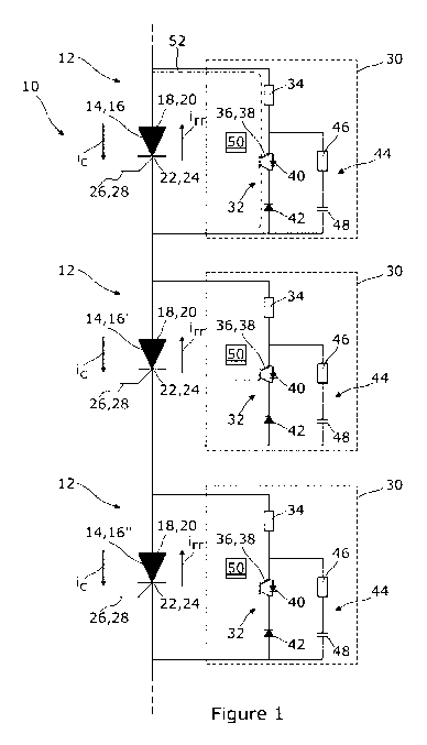
Figure 1 shows a portion of a semiconductor switching string according to a
first
embodiment of the invention; and
Figure 2 illustrates current and voltage levels during operation of a given
semiconductor
switching assembly which forms a part of the semiconductor switching string
shown in
Figure 1.
A semiconductor switching string according to a first embodiment of the
invention is
designated generally by reference numeral 10, as shown in Figure 1.
The semiconductor switching string 10 includes a plurality of series-connected
semiconductor switching assemblies 12, each of which semiconductor switching
assembly 12 includes a main semiconductor switching element 14. Only three
semiconductor switching assemblies 12 are shown in Figure 1 although the
semiconductor switching string 10 may include many tens of such semiconductor
switching assemblies 12 and even many hundreds of semiconductor switching
assemblies 12.
In the embodiment shown each main semiconductor switching element 14 is a main
thyristor 16, 16', 16", although in other embodiments of the invention a
different main
semiconductor switching element 14 may be used such as a diode, Light-
Triggered
Thyristor (LTT), Gate Turn-Off thyristor (GTO), Gate Commutated Thyristor
(GCT)
or Integrated Gate Commutated Thyristor (IGCT). Preferably the main
semiconductor
switching element 14 is optimised for lowest conduction (on-state) losses at
the expense
of other parameters such as turn-off performance characteristics.
Each main thyristor 16, 16', 16" shown includes an anode 18 which defines a
first
terminal 20, a cathode 22 which defines a second terminal 24, and a gate 26
that defines
a control terminal 28 via which the main thyristor 18 may be switched on.
More particularly, each main thyristor 16, 16', 16" is naturally commutated,
and so
while it can be turned on via the aforementioned gate 26, i.e. the control
terminal 28, it
7
CA 02998800 2018-03-15
WO 2017/055243
PCT/EP2016/072911
can only be turned off by arranging the circuit in which it is located to
force the current
flowing through it to fall to zero and then maintaining a period (typically of
a few
hundred microseconds) during which it is reverse-biased, i.e. during which a
negative
voltage is applied between the first and second connection terminals 20, 24.
When switched on each main thyristor 16, 16', 16" operates in a conducting
mode in
which a conducting current ic flows from the first terminal 20 to the second
terminal 24.
While turning off, i.e. while naturally commutating, each main thyristor 16,
16', 16"
transitions from a reverse recovery mode, in which a reverse recovery current
in. flows
from the second terminal 24 to the first terminal 20, to a blocking mode in
which no
current flows between the first and second terminal 20, 24.
Each main semiconductor switching element 14, i.e. each main thyristor 16,
16', 16",
has an active auxiliary circuit 30 electrically connected between the
aforementioned
first and second terminals 20, 24 so as to lie in parallel with the
corresponding main
semiconductor switching element 14. Within the context of the invention
'active' is
intended to mean that the auxiliary circuit can be controlled at will, i.e.
switched
between operative and inoperative configurations, e.g. by an electronic
programmable
control unit, rather than its use being controlled by passive components such
as resistors
and capacitors which are able only to react to changes in a current flowing
therethrough
or a voltage applied thereto and are unable make an operational decision
independently
of such a current or voltage.
Each auxiliary circuit 30 includes an auxiliary semiconductor switching
element 32 and
a resistive element 34 which are connected in series with one another.
In the embodiment shown, each auxiliary semiconductor switching element 32
includes
a single self-commutated semiconductor switch 36, i.e. a semiconductor switch
36 that
can be switched on and off via a signal applied to a gate control within the
switch 36.
By way of example, the semiconductor switch 36 shown is an insulated-gate
bipolar
transistor (IGBT) 38, but other possible self-commutated semiconductor
switches 36
include metal-oxide-semiconductor field-effect-transistors (MOSFETs), gate
turn-off
8
CA 02998800 2018-03-15
WO 2017/055243
PCT/EP2016/072911
transistors (GT0s), bipolar junction transistors (BJTs) and integrated gate-
commutated
thyristors (IGCTs).
Each IGBT 38 is connected in anti-parallel with the corresponding main
thyristor 16,
16', 16" and itself includes an anti-parallel diode 40 connected thereacross.
In addition, each auxiliary semiconductor switching element 32 shown includes
a
series-connected diode 42 to provide a reverse current blocking capability.
Each
auxiliary semiconductor switching element 32 also has a snubber circuit 44
connected
in parallel across both the self-commutated switch 36, i.e. the IGBT 38, and
the series-
connected diode 42. Each snubber circuit 44 includes a snubber resistor 46 and
a
capacitive component, in the form of a snubber capacitor 48, which are
connected in
series with one another. In other embodiments of the invention, some or all of
the
snubber circuits may be connected in parallel across only the self-commutated
switch.
In other embodiments of the invention (not shown) one or more of the auxiliary
semiconductor switching elements 32, e.g. those in which the corresponding
self-
commutated semiconductor switch 36 is able to provide a symmetrical voltage
blocking
capability, may omit the series-connected diode 42. In such arrangements the
corresponding self-commutated semiconductor switch 36 is likely to be based on
a
wide-band gap material such as silicon carbide.
In still further other embodiments of the invention (also not shown) one or
more of the
auxiliary semiconductor switching elements 32 may include a plurality of self-
commutated semiconductor switches 36 which are connected in series with one
another.
Each such semiconductor switch 36 may include its own anti-parallel diode 40
and
associated series-connected diode 42. Such multiple semiconductor switch 32
and diode
40, 42 combinations may each have their own respective snubber circuit
connected in
parallel thereacross, or a number of semiconductor switch 32 and diode 40, 42
combinations may instead have a single snubber circuit connected in parallel
thereacross.
9
CA 02998800 2018-03-15
WO 2017/055243
PCT/EP2016/072911
Returning the embodiment partially shown in Figure 1, each resistive element
34 is in
the form of a resistor, although other types of resistive element may also be
used. Each
resistor has a resistance value which, in use, results in the amount of
current that
continues to flow through the resistive element 34 once the corresponding main
thyristor 16, 16', 16" is operating in its blocking mode, i.e. once the
corresponding main
thyristor 16, 16', 16" has turned off completely, equating to at least 10%,
and preferably
between 30% and 40%, of the peak reverse recovery current iiT flowing through
the said
corresponding main thyristor 16, 16', 16" when it is operating in its reverse
recovery
mode.
More particularly each resistive element 34 has the same resistance value (so
far as is
possible with very tight manufacturing tolerances) which, by way of example,
would
lie in the range of 75E2 to 90E2. The resistance value could, however, lie
outside the
aforementioned range depending on the type of main thyristor 16, 16', 16" and
the peak
reverse recovery current iiT associated with the said main thyristor 16, 16',
16" included
in the semiconductor switching string 10.
As well as the plurality of semiconductor switching assemblies 12 mentioned
hereinabove, the semiconductor switching string 10 of the invention also
includes a
control unit 50 which is operatively connected with each auxiliary
semiconductor
switching element 32.
Such a semiconductor switching string 10 may, as shown in Figure 1, include a
plurality
of individual control units 50, each of which is arranged in direct, operative
communication with a single corresponding semiconductor switching element 32.
Alternatively a plurality of, or indeed all of, the semiconductor switching
elements 32
within a given semiconductor switching string 10 may share a single control
unit (not
shown).
In the embodiment shown, each control unit 50 is configured to switch the
corresponding auxiliary semiconductor switching element 32 into a conducting
state,
i.e. turn on the self-commutated semiconductor switch 36 located therein, to
create an
CA 02998800 2018-03-15
WO 2017/055243
PCT/EP2016/072911
alternative current path 52 (only one such path shown in Figure 1 for clarity)
between
the first and second terminals 20, 24 of the corresponding main thyristor 16,
16', 16",
via which current is diverted through the corresponding resistive element 34.
In addition, each control unit 50 is further configured to have all of the
auxiliary
semiconductor switching elements 32, i.e. all of the self-commutated
semiconductor
switches 36 therein, in their conducting state simultaneously while each main
semiconductor switching element 14, i.e. each main thyristor 16, 16', 16", is
first
operating in its reverse recovery mode and then in its blocking mode.
Accordingly, each control unit 50 is configured to turn on its associated
auxiliary
semiconductor switching element 32 while the corresponding main thyristor 16,
16',
16" is operating in its reverse recovery condition (although in other
embodiments of the
invention this may be prior to the corresponding main thyristor 16, 16', 16"
operating
in its reverse recovery condition), and to turn the said associated auxiliary
semiconductor switching element 32 off once the said corresponding main
thyristor 16,
16', 16" has completed its reverse recovery and is operating in its blocking
mode.
In other embodiments of the invention, however, the or each control unit 50
may be
configured to have all of the auxiliary semiconductor switching elements 32 in
their
conducting state simultaneously only while each main semiconductor switching
element 14 is operating in one or other of its reverse recovery mode and its
blocking
mode.
As such, one or more of the control units 50 in other embodiments of this
nature may
instead be configured to turn on its associated auxiliary semiconductor
switching
element 32 at the same time as the main thyristor 16, 16', 16" begins to
operate in its
blocking mode.
Each control unit 50 may be configured in each of the aforementioned manner by
being
individually programmed and able to coordinate its operation with each of the
other
11
CA 02998800 2018-03-15
WO 2017/055243
PCT/EP2016/072911
control units 50, or by being instructed to operate as required by, e.g. a
higher-level
controller.
In embodiments including only one, or a reduced number of shared control
units, the or
each such control unit may be configured in a similar way, i.e. individually
programmed
and able to coordinate its operation, or instructed to operate as required by
some higher-
level entity.
Returning to the embodiment shown, a practical way in which the control units
50 are
able to ensure that all of the auxiliary semiconductor switching elements 32
are in their
conducting state simultaneously while each main thyristor 16, 16', 16" is
operating in
both its reverse recovery mode and then its blocking mode, is to configure the
control
units 50 to have all of the auxiliary semiconductor switching elements 32 in
their said
conducting state simultaneously a predetermined period of time after a given
reference
point in the operating cycle of the semiconductor switching string 10.
Possible reference points within such an operating cycle are:
(a) the
dispatch of a switch-on signal, e.g. from a higher-level controller, to
each main semiconductor switching element 14, i.e. each main thyristor 16,
16', 16";
(b) the dispatch of
a switch-on signal, e.g. from a higher-level controller, to
a further semiconductor switching string with which the semiconductor
switching string
10 of the invention is operatively associated, e.g. a further semiconductor
switching
string in a different limb portion of a HVDC power converter in which the
semiconductor switching string 10 of the invention is located; or
(c) a zero voltage
arising across one or both of the main thyristor 16, 16',
16" and the semiconductor switching string 10.
In any event, each control unit 50 is additionally configured to subsequently
turn off
simultaneously all of the auxiliary semiconductor switching elements 32. This
simultaneously stops the flow of current through each auxiliary circuit 30 and
its
associated resistive element 34, current which was previously flowing via the
12
CA 02998800 2018-03-15
WO 2017/055243
PCT/EP2016/072911
associated alternative current path 52 temporarily created by turning on the
said
auxiliary semiconductor switching element 32.
As indicated above, each control unit 50 is configured to turn off its
associated auxiliary
semiconductor switching element 32 after the corresponding main thyristor 16,
16', 16"
has completed its reverse recovery, i.e. once the corresponding main thyristor
16, 16',
16" is operating in its blocking mode.
However, in other embodiments of the invention, one or more of the control
units 50
may be configured to turn off its associated auxiliary semiconductor switching
element
32 while the corresponding main thyristor 16, 16', 16" is in the late stages
of reverse
recovery, i.e. slightly before the main thyristor 16, 16', 16" begins to
operate in its
blocking mode and as the reverse recovery current irr flowing through the main
thyristor
16, 16', 16" approaches zero.
Again, a practical way in which the control units 50 can simultaneously turn
off all of
the auxiliary semiconductor switching elements 32 at a desired point is to do
so
following an event experienced within the semiconductor switching string 10.
Such an event may be one of:
(a) the turning on of each auxiliary semiconductor switching element 32;
(b) a peak voltage arising across one or both of the corresponding main
thyristor 16, 16', 16" and the semiconductor switching string 10;
(c) the receipt of a dedicated turn-off signal for each auxiliary
semiconductor switching element 32 from a higher-level controller;
(d) a stabilisation of the current flowing through each auxiliary circuit
30;
Or
(e) a stabilisation of the voltage across one or both of the main thyristor
16,
16', 16" and the semiconductor switching string 10.
In use the semiconductor switching string 10 illustrated in Figure 1 operates
as follows,
with reference being made to Figure 2 which shows the current flowing through
a main
13
CA 02998800 2018-03-15
WO 2017/055243
PCT/EP2016/072911
thyristor 16, 16', 16", i.e. a thyristor current ithy, and the current flowing
through the
corresponding auxiliary circuit 30, i.e. an auxiliary current Lux, within a
given
semiconductor switching assembly 12 of the switching string 10, as well as the
current
flowing through the switching string 10 itself, i.e. a string current i
-string.
While each main semiconductor switching element 14, i.e. each main thyristor
16, 16',
16", is switched on and operating in its respective conducting mode (as
illustrated
during a first period 54 in Figure 2) a positive conducting current ic is able
to flow from
the first terminal 20 to the second terminal 24 of each main thyristor 16,
16', 16", and
hence through the semiconductor switching string 10 as a whole via each
semiconductor
switching assembly 12. Hence each of the thyristor current ithy and the string
current
istring is equal to the conducting current ic. Meanwhile each auxiliary
semiconductor
switching element 32 is switched off, i.e. is in its non-conducting state, and
so the
current flowing through each corresponding auxiliary circuit 30, i.e. the
auxiliary
current Lux is zero.
When each main thyristor 16, 16', 16" is turned off, i.e. when the conducting
current ic
flowing through them is forced to zero and they become reverse-biased, they
first
operate in their reverse recovery mode (as illustrated during a second period
56 in
Figure 2) in which a reverse recovery current irr is able to flow from the
second terminal
24 to the first terminal 20 thereof.
Initially during this second period 56 both the thyristor current ithy and the
string current
istring are equal to the reverse recovery current irr and the auxiliary
current Lux remains at
zero.
The turn on 58 of each auxiliary semiconductor switching element 32 takes
place prior
the corresponding main thyristor 16, 16', 16" beginning 66 to support a
voltage and
while the corresponding main thyristor 16, 16', 16" is operating in its
reverse recovery
mode. Such turn on 58 causes current, i.e. current flowing from the preceding
semiconductor switching assembly 12 in the semiconductor switching string 10,
to be
diverted through the corresponding auxiliary circuit 30 and the resistive
element 34
14
CA 02998800 2018-03-15
WO 2017/055243
PCT/EP2016/072911
lying therein. Such current is initially shared between the main thyristor 16,
16', 16"
and the corresponding auxiliary circuit 30.
Thereafter, as each such main thyristor 16, 16', 16" continues to recover,
i.e. transitions
to being able to block current while operating in its blocking mode, the
auxiliary current
faux, i.e. the current flowing through both the semiconductor switch 36 and
resistive
element 34 of each auxiliary circuit 30, increases while the thyristor current
ithy falls.
During the same period the string current i
-string increases and then falls.
Once each main thyristor 16, 16', 16" has transitioned to its blocking mode
(as
illustrated during a third period 60 in Figure 2) no current flows between the
first and
second terminals 20, 24 thereof, and hence the thyristor current ithy is zero.
In the
meantime all the auxiliary semiconductor switching elements 32 remain
simultaneously
in their conducting state, i.e. all of the auxiliary semiconductor switching
elements 32
and their respective associated auxiliary circuit 30 are in an operative
configuration at
the same time, and so the current continuing to flow through the semiconductor
switching string 10 is made up solely of the current flowing through each
auxiliary
circuit 30. As a consequence the string current i
-string becomes equal to the auxiliary
current Lux.
At this stage the semiconductor switching string 10 is essentially a string of
auxiliary
circuits 30 since each main thyristor 16, 16', 16" has recovered its voltage
blocking
capability, i.e. is operating in its blocking mode, and so effectively defines
an open
circuit. As a consequence, the voltage across each main thyristor 16, 16',
16", i.e. each
main semiconductor switching element 14, is determined solely by the voltage
across
the resistive element 34 in the corresponding auxiliary circuit 30 which is
electrically
connected between the first and second terminals 20, 24 of the said main
thyristor 16,
16', 16".
Moreover, since the resistance value of each resistive element 34 is the same,
the
voltage v, v', v" across each main thyristor 16, 16', 16" is also the same, as
illustrated
CA 02998800 2018-03-15
WO 2017/055243
PCT/EP2016/072911
in Figure 2. Consequently the voltage across the whole semiconductor switching
string
is shared equally amongst the various main thyristors 16, 16', 16".
Simultaneous turn off 62 of each auxiliary semiconductor switching element 32,
i.e.
5 each self-
commutated semiconductor switch 34, results in a temporary voltage
overshoot across each said auxiliary semiconductor switching element 32 and
associated snubber circuit 44, which in turn appears as a voltage overshoot 64
across
each corresponding main thyristor 16, 16', 16". However, current is stopped
from
flowing through each corresponding auxiliary circuit 30 and so the auxiliary
current Lux
10 drops to
zero and the voltage v, v', v" across each main thyristor 16, 16', 16" returns
to
being the same, equal shared value.
In still further embodiments of the invention (not shown) one or more of the
semiconductor switching assemblies may include a modified auxiliary
semiconductor
switching element in which the series-connected diode is replaced by a further
self-
commutated semiconductor switch which is connected in an opposite sense to the
original self-commutated semiconductor switch, such that the modified
auxiliary
semiconductor switching element is able to provide a symmetrical voltage
blocking
capability. In such embodiments, the control unit operatively associated with
the
modified auxiliary semiconductor switching element may be still further
configured to
have the said modified auxiliary semiconductor switching element in its
conducting
state while the corresponding main thyristor is operating in its conducting
mode.
Such switching on of the modified auxiliary semiconductor switching element
provides
a current discharge path for the capacitor within a snubber circuit connected
in parallel
across the said modified auxiliary semiconductor switching element, through
the
auxiliary semiconductor switching element rather than through the
corresponding main
thyristor, and so reduces the current stress that the main thyristor
experiences compared
to that it would otherwise experience when switching into its conducting mode,
i.e.
when turning on.
16
CA 02998800 2018-03-15
WO 2017/055243
PCT/EP2016/072911
Once the capacitor has discharged the current flowing through the auxiliary
semiconductor switching element falls to zero and the auxiliary semiconductor
switching element can be turned off in order to save power. It can be turned
on again,
as needed, nearer the time of the corresponding main semiconductor switching
element
operating in its reverse recovery mode. Alternatively it can remain on for the
whole
time for which the corresponding main semiconductor switching element operates
in
its conducting mode.
17