Note: Descriptions are shown in the official language in which they were submitted.
CA 02999372 2018-03-21
THIN FILM COATING LAYER COMPOSITION AND COATING METHOD
FIELD OF THE INVENTION
This invention relates to the field of solution-based film coating of
substrates like polyester film, polyimide film, polyvinyl chloride film, semi-
embossed film, polyvinyl chloride film and like, and is specifically concerned
with coating substrates with a coating based on SU-8 and poly(4-vinyl
pyridine) (P4VP).
DESCRIPTION OF THE PRIOR ART
Recently, flexible electronics are gaining increasing research interest due to
their promising applications in many practical fields, such as wearable
electronics, portable devices, medical implants, etc.( S. R. Forrest, Nature
2004,
428, 911-918.; D.H. Kim, N.S. Lu, R. Ma, Y.S. Kim, R.H. Kim, S.D. Wang, J. Wu,
S. M. Won, H. Tao, A. Islam, K. J. Yu, T. I. Kim, R. Chowdhury, M. Ying, L. Z.
Xu,
M. Li, H. J. Chung, H. Keum, M. McCormick, P. Liu, Y. W. Zhang, F. G.
Omenetto, Y. G. Huang, T. Coleman, J. A. Rogers, Science 2011, 333, 838.; Y.
G. Sun, J. A. Rogers, Adv. Mater. 2007,19, 1897-1916.) Flexible circuit, as
"blood circulation system" of flexible electronic products, plays an
especially
important role. Attributed to flexible digital processing mode and a rapid
scalable
manner, nowadays printing techniques are providing a powerful tool for the
fast
design and fabrication of different patterns. The application of printing
technique
in fabricating flexible electronics will undoubtedly open a new door for the
production of flexible circuits. Since the printer can make patterns in a high-
efficiency mode, the conversion of printed patterns into conductive circuits
naturally becomes the crux of the question. Electroless metal deposition
(ELD),
1
CA 02999372 2018-03-21
relying on an autocatalytic redox reaction to deposit thin-layer metal on a
catalyst-
preloaded substrate, provides a good solution to this question. (R. S. Guo, Y.
Yu,
Z. Xie, X. Liu, X. Zhou, Yufan Gao, Z. Liu, F. Zhou, Y. Yang, Z. Zheng, Adv.;
M.
S. Miller, H. L. Filiatrault, G. J. E. Davidson, M. Luo, T. B. Carmichael, J.
Am.
Chem. Soc. 2010,132, 765-772.; T. Zhang, X. Wang, T. Li, Q. Guo and J. Yang,
J. Mater. Chem. C, 2014, 2, 286-294.) With the assistance of printing
techniques,
active catalyst can be deployed on the specified area of flexible substrate,
and
thus induce the formation of as-required metal pattern. However, as an open
problem, it is known that untreated flexible plastics cannot well grasp
catalyst
moieties due to lacking binding sites, and simple physical absorption usually
results in the diffusion of catalyst into ELD solution and poor adhesion of as-
deposited metal to the substrate, and further leads to bad coating quality
especially when metal layer become thick, such as delamination and metal bump,
and thus it is necessary to modify the surface of flexible substrate for
effective
uptake of catalyst moieties and improved adhesion of as-deposited metal to the
substrate.
Currently, there are mainly two general approaches for surface modification
of plastics, which can be classified into surface reforming and surface
addition.
Surface reforming refers to changing surface roughness or making active
functional groups on the original surface via in-situ oxidizing reaction, such
as
chemical etching, oxygen plasma. (A. Garcia, T. Berthelot, P. Viel, A.
Mesnage,
P. Jegou, F. Nekelson, Sebastien Roussel, S. Palacin, ACS Appl. Mater.
Interfaces 2010, 2, 1177-1183.; J. B. Park, J. S. Oh, E. L. Gil, S. J. Kyoung,
J. T.
Lim, G. Y. Yeom, J. Electrochem. Soc., 2010, 157, D614-D619.) Surface addition
means to add an extra active layer onto existing plastics surface, typically
including polymer grafting, (A. Garcia, J. Polesel-Maris, P. Viel, S. Palacin,
T.
2
CA 02999372 2018-03-21
Berthelot, Adv. Funct. Mater. 2011, 21, 2096-2102.; A. Garcia, T. Berthelot,
P.
Viel, P. Jegou, S. Palacin, ChemPhysChem 2011, 12, 2973 ¨ 2978.) surface
silanization (S. Sawada, Y. Masuda, P. Zhu, K. Koumoto, Langmuir 2006, 22,
332-337.; Y. Chang, C. Yang, X.-Y. Zheng, D.-Y. Wang, Z.-G. Yang, ACS Appl.
Mater. Interfaces 2014, 6, 768-772.) and layer-by-layer deposition of
polyelectrolytes, (K. Cheng, M.-H. Yang, W. W. W. Chiu, C.-Y. Huang, J. Chang,
T.-F. Ying, Y. Yang, Macromol. Rapid Commun. 2005, 26, 247-264.; T. C. Wang,
B. Chen, M. F. Rubner, R. E. Cohen Langmuir 2001,17, 6610-6615.) etc.
As is described, herein there are mainly two purposes for surface
modification of flexible substrates, namely realizing selective and efficient
uptake
of catalyst moieties, and improving the adhesion between the substrate and
metal. Consequently, surface modification of plastic substrate should at least
take
care of these two aspects. On the one hand, modified surface must contain the
functional groups that can effectively grasp catalyst moieties; on the other
hand,
modified surface should be chemically resistant to electroless plating bath
and
can further play a buffer layer between original substrate and metal for
better
adhesion. A lot of reports have indicated that modified surface by different
methods can enhance the compatibility of metal and organic plastics, but most
of
them are still far away from scalable low-cost application, either due to
complex
or environment-unfriendly technological process, or because of the difficulty
in
scaling up. For instance, typical chromium-containing etching agent for
surface
modification of printed circuit board have been prohibited in many countries
due
to its harm to the environment; ligand-containing silane modified film is not
acid or
alkali resistant, and thus cannot withstand long-time electroless metal
deposition
because most of metal plating bath is relatively alkali; the grafting of
polymer
brush usually involves complex steps and harsh requirements for experimental
3
CA 02999372 2018-03-21
conditions; layer-by-layer polyelectrolyte deposition is extremely slow and
low-
efficiency and will cost too much time due to tens of repeated coating
operation.
Therefore, these methods are not suitable for surface modification of large-
area
flexible plastics on a large scale.
P4VP molecules can also be directly coated on the surface of substrate, but
simple physical absorption usually results in poor adhesion of modified layer.
Thus there is a must to develop a more cost effective method for enhanced
adhesion of P4VP molecules on the substrates. As early as 1980s, it had been
found that pyridine molecules can help to cure epoxy, (Xue, G.; Ishida, H.;
Konig,
J. L. MakromoL Chem., Rapid Commun. 7 (1986) 37; ldem. , Angew. Makromol.
Chem. 142 (1986) 17) and subsequently P4VP also shows the ability to cross
link
epoxy. (Meng, F.; Zhang, W.; Zheng, S. J. Mater. ScL 40 (2005) 6367-6373)
Based on this mechanism, in this invention, we employ epoxy to cross link P4VP
molecules. On the one hand, epoxy has strong reactivity and can form good
chemical and mechanical adhesion with polymer substrate; on the other hand,
epoxy molecules can also react with each other and P4VP molecules to buildup
cross-linked polymer network on the substrate.
SUMMARY OF THE INVENTION
It is an object of the invention to provide a simple one-step solution-based
coating method for scalable surface modification of the films with different
sizes,
which will largely decrease the cost of film treatment while meeting the
requirements for high-quality metal deposition.
Another object of the invention is to provide an efficient coating to make
sure that the deposited copper layer with the thickness more than 7 microns
can
be easily made on the surface of flexible substrate without any delamination,
4
CA 02999372 2018-03-21
which is difficult to achieve in other modified surface may attributed to our
thicker
modified layer produced by dip coating for better adhesion promotion.
Another object of the invention is to provide a printing friendly film coating
which enables laser printing, inkjet printing, screen printing, gravure
techniques
and like to make the mask or to directly deposit functional catalyst on the
film
surface, in order to induce the formation of metal pattern.
These and other objects are accomplished by our invention which is
described below.
We have invented a solution-based method for the fast surface modification
of flexible plastics. The coating process can be completely executed under
atmosphere at a relatively low temperature, which renders this method suitable
for
large-scale surface modification of large-area flexible substrates. As-
employed
surface modifier was composed of polymer ligands and reactive adhesive, and
they cannot only react with each other to form cross-linked polymer network,
and
also reactively bond with the substrates to produce a highly adhesive alkali
resistant ligand layer on the surface of substrates for the selective and
effective
uptake of catalyst moieties.
With the invented coating composition and through electroless copper
plating, high-quality copper layer with controllable thickness can be
deposited on
the flexible substrates. Ultra-thick copper layer (> 7 pm) can be achieved by
increasing the plating time, which well overcome the existing problem of thick
copper deposition on flexible substrate and open a new way for real industrial
production and application of flexible circuits.
Furthermore, double-side flexible circuits with higher integration can be
fabricated fast on modified plastics, which will save more cost and space for
5
CA 02999372 2018-03-21
flexible electronic devices. In addition, this method for surface modification
of
flexible plastics can further be extended to other substances, such as 3D
objects,
paper, cloth, wood, and so on, which will provide a powerful tool for the
metallization of isolated materials.
BRIEF DESCRIPTION OF THE DRAWINGS
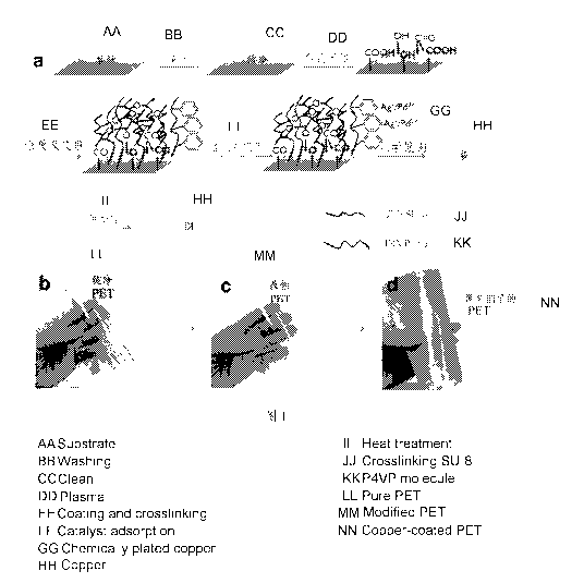
Figure la P4VP using SU-8 and PET film coated with a mixture of a
schematic flow diagram;
Figure lb is a photograph of a pure transparent PET film is thin;
Figure lc is a PET film using SU-8 and the P4VP modified;
Figure id lh is covered by a PET film with a copper plating copper layer.
Figure 2a P4VP respectively, and SU-8 P4VP composite coating, and SU-8
P4VP composite coating without NaOH treatment, after treatment P4VP 1M NaOH
1 hour after curing SU-8 and the composite coating FT-IR Spectrum;
Figure 2b is a diagram of the contact angle of pure water and the PET film;
Figure 2c is a schematic view of a contact angle of water with the modified
PET film;
Figure 2d is a schematic view of water treatment and post-curing modified
PET film contact angle of sodium hydroxide;
Figure 3a is a laser printer to produce a flexible circuit schematic printed
on
the surface modification of toner base reticle;
Figures 3b and 3c are two circuit patterns on the two different sides of the
same piece of PET film;
6
CA 02999372 2018-03-21
Figures 4a and 4b are SEM images of the surface of a copper layer of
copper over 10min;
Figures 4c and 4d are 30min, and lh after the copper plating layer on the
surface SEM image;
Figure 4e and 4f respectively through lh, 12h copper deposition layer of
copper cross-sectional SEM image.
Figure 5 shows the surface resistivity of the copper layer versus plating
time and a copper plating layer thickness increases with plating time.
Figures 6 shows cross-sectional SEM images of layers with different
thickness of the copper plating of time.
The following examples illustrate the present invention and its use in the
manufacture of printed electronics.
DETAILED DESCRIPTION OF THE INVENTION
In this invention, based on the thermally initiated cross-linked reaction
between epoxy and pyridine rings, we employ SU-8 molecules and poly (4-vinyl
pyridine) (P4VP) as the main components of film-making solution, in which SU-8
behaves as curing agent and adhesives, and P4VP acts as metal ligand, and
then dip coat on the surface of plastic substrate followed by low-temperature
curing.
Preferably the inventive film coating composition includes one or more of
the following components: poly (4-vinyl pyridine), SU-8, 1, 4-dioxane, 2-
propanol
and ethanol.
7
CA 02999372 2018-03-21
In accordance with the invention, a method of coating substrates, such as
polyester film, polyimide film, polyvinyl chloride film, semi-embossed film,
polyvinyl chloride film, and like with a film coating, comprises the steps of
dissolving 1) poly(4-vinyl pyridine), 2) SU-8 into 1,4-dioxane and 2-propanol
mixture to form an uniform coating solution, applying an effective amount of
the
coating solution onto the substrates using dip-coating, spin-coating, blade
coating, inkjet printing, screen printing and like to form an uniform film
coating on
the substrates, and baking the film coating on the substrates in an oven,
optionally, but preferably, one or more of the following components is/are
mixed
into the coating solution with the poly(4-vinyl pyridine), SU-8, 1,4-dioxane
and 2-
propanol to achieve the desired properties such as surface tension, viscosity
etc.
for different coating techniques mentioned above: glycerol, ethanol, polyvinyl
pyrrolidone, polyethylene glycol, surfactant and like.
Poly (4-vinyl pyridine) (P4VP) has been a good candidate of surface
modifiers used for uptake of transitional metal ions attributed to its good
alcohol
solubility, chelating ability, and pyridine ligands-bearing. 4-vinyl pyridine,
as a kind
of reactive monomer, can be used to modify substrate surfaces by in-situ
polymerization under UV or plasma.
SU-8 plays a bridging agent to anchor P4VP molecules on the substrate
surface. Attributed to strong covalent bonding, as-formed coating layer will
have a
good adhesion to the substrate. Furthermore, as a result of ring opening
reaction
of epoxide groups, carbon-oxygen bonds will be the dominant bonding type. In
contrast to silicon-oxygen bond and ester groups in other polymer grafting,
carbon-oxygen ether bonds are more alkali resistant. It is absolutely
beneficial for
subsequent electroless copper deposition in basic bath.
8
CA 02999372 2018-03-21
Preferably, the poly (4-vinyl pyridine) (P4VP) is dissolved in 2-propanol to
form a uniform solution, the preferred concentration is 1 w/v% - 8 w/v%, more
preferred 3 w/v% - 6 w/v%. Preferably, the SU-8 is dissolved in 1, 4-dioxane
to
obtain a uniform solution as well, the preferred concentration is 0.1 w/v% - 2
w/v%, more preferred 0.3 w/v% - 1 w/v%. Preferably the two solutions are mixed
to get a transparent coating solution. The preferred solution contains 0.5
w/v%
4 w/v% P4VP and 0.05 w/v% - 1 w/v% SU-8, more preferred 1.5 w/v% - 3 w/v%
P4VP and 0.15 w/v% - 0.5 w/v% SU-8.
The ranges of each components of the coating composition of the invention
are as follows, by weigh/volume:
COMPONENT ACCEPA TABLE PREFERRED RANGES
RANGES (wlv %) (wlv %)
poly (4 vinylpyridine) (P4VP) 0.5 to 4 1.5 to 3
SU-8 0.05 to 1 0.15 to 0.5
1,4-dioxane 47 to 50 48.25 to 49.75
2-propanol 47 to 50 48.25 to 49.75
The following examples illustrate the invention and its use in the fabrication
of printed electronics.
EXAMPLE 1
The poly (4-vinyl pyridine) is dissolved in 2-propanol to form 4 w/v%
solution, and SU-8 is dissolved in 1,4-dioxane to obtain 0.4 w/v% solution.
Then
the two solutions were mixed at 1:1 ratio to get a transparent solution. The
final
solution contains 2 w/v% P4VP and 0.2 w/v% SU-8.
Transparent PET film is cleaned by the mixed solution of 1:1 ethanol and
acetone, and then is treated with oxygen plasma followed by dip coating or
directly
immersed into the film-making solution for dip-coating without oxygen plasma
9
CA 02999372 2018-03-21
introduced. After 30 seconds, the film is drawn out of the solution slowly and
dried
in air. In the next, the coated film is put into oven of 120 C for 20mins for
in-situ
cross-linking reaction of P4VP and SU-8. The thickness of coated layer can be
controlled by adjusting the concentration of P4VP and SU-8 in mixed solvent of
2-
propanol and 1, 4-dioxane.
Upon completion of the coating process, the PET film shows a smooth
surface with excellent surface uniformity. The film coating on the PET
substrate
possesses an excellent long-lasting uniformity, minimal tackiness, good film
adhesion.
COMPONENT PERCENTAGE AMOUNT
poly (4-vinyl pyridine) (P4VP) 2 w/v % 2 grams
SU-8 0.2 w/v % 0.2 grams
1,4-dioxane 50 v/v % 50 mL
2-propanol 50 v/v % 50 mL
To demonstrate the functionality of the invented coating, AgNO3 was
dissolved into deionized water to get 1w/v% AgNO3 solution, and the coated PET
film is soaked into the AgNO3 solution for 10 seconds for the uptake of silver
ions.
Then the film is washed several times by water to remove free silver ions
without
bonding with pyridine ligands. The film is dried and put into electroless
copper
plating bath for different time. Electroless copper plating bath consists of
CuSO4.5H20 (14 g/L), NaOH (12 g/L), potassium sodium tartrate (16 g/L),
EDTA.2Na (20 g/L), HCHO (16.5 mL/L), 2, 2'-dipyridyl (20 mg/L), and potassium
ferrocyanide (10 mg/L).
Figure la shows the schematic flow of coating PET film by P4VP&SU-8
composites. Oxygen plasma was employed for surface activation to introduce
CA 02999372 2018-03-21
oxygen-containing groups and free radicals on the surface. In principle, these
active groups excited by plasma can react with the epoxide groups of SU-8 to
form covalent bonding. Figure lb and lc present the digital photos of pristine
transparent PET film and P4VP and SU-8 modified PET film respectively. It can
be seen that, although coated by a layer of P4VP and SU-8 composites, the film
is still flexible and highly transparent. The introduction of thin-layer of
P4VP and
SU-8 composites did not affect the appearance and mechanical properties of
PET film a lot.
To further demonstrate the inner principle of the invented coating
composition, FT-IR analysis is performed using FT-IR NICOLET 6700 (Thermo
Scientific Co.). The contact angle of water with different substrates was
measured
by Rame-Hart Contact Angle Goniometer.
Figure 2a shows FT-IR spectrum of P4VP and its composites coated on
the substrates. Different spectra present some discrepancies in peak position
and
intensity. In reference of standard infrared absorption of different
functional
groups, we can get much information from the spectra. The peaks located in 871
cm-1 well matches with the absorption of benzene ring, which indicates the
introduction of SU-8 in composite coating layer. We can also see that, after
curing, the epoxide groups at 915 cm -I almost completely disappear, which
demonstrate that strong reactive epoxide groups were nearly consumed up at
relatively high curing temperature. Plus, the vibration absorption at 1664cm-I
that
belongs to amide groups was enhanced, which further indicated that cross-
linked
reaction occurred between pyridine groups and epoxide groups, and new amide
groups-bearing products were formed, which is consistent with other research
reports. In addition, there are two strong absorption peaks between 1500 cm-1
and 1600 cm-1 for all the coating layers, which belong to pyridine rings of
P4VP
11
CA 02999372 2018-03-21
molecules. Before and after curing, the strength and position of the two peaks
did
not almost change a lot. It indicates that, during curing process, only a
small
amount of pyridine ligands are consumed by epoxide groups due to much higher
content of P4VP in the composites, and a lot of residual pyridine ligands will
be
available for the uptake of catalyst moieties in the following steps. Figure
2a also
presents FT-IR spectrum of cured P4VP and SU-8 composite layer treated by 1
M NaOH for lh. The spectrum is nearly the same with the sample untreated by
NaOH, which means that the initial coating layer was still well maintained on
the
surface of the substrate, and can withstand the erosion of basic solution to
some
extent. Figure 2b show the contact angle of water with pristine PET film, and
it is
about 46 degree. After surface modification, the contact angle increase to
about
77 degree maybe due to the introduction of hydrophobic SU-8. After being
treated by NaOH, the contact angle decreases slightly but is still much larger
than
that on pristine PET.
Evidently, the invented coating changes the surface energy of PET, and
makes PET more hydrophobic. Perhaps enhanced hydrophobicity is not
favorable for the wettability of film, but can prevent excessive spreading of
aqueous ink, and will be helpful for improving the resolution of printed ink
on the
substrate once the modified film was used as the substrate of inkjet printing.
In the following examples 2, a functional circuits are fabricated based on the
invented coating composition. SEM investigation are conducted to further
demonstrate the functionality of this invention.
EXAMPLE 2
The coating composition and coating methods are exactly the same as that
in example 2. The coated PET film is activated by 1w/v% AgNO3 solution by
12
CA 02999372 2018-03-21
soaking the film into the solution for 10 seconds, and then dried for
printing.
Commercial HP laser printer 6700 is used for the printing of toner mask. After
printing, the film is put into the oven of 90 C for 1 min for the
stabilization of toner
mask, and then soaked into electroless copper plating bath for different time.
The
exposed area will be coated by copper, and copper cannot be formed in the
place
covered by mask due to the deactivation of the catalyst. After obtaining
certain
thickness of copper pattern, the mask layer can be washed in acetone by
sonication or washed directly by dichloromethane or tetrahydrofuran.
Figure 3 shows the detailed schematic diagram for the production of
flexible circuits by employing laser printer to print toner mask on the
modified
substrates. Figure 3b and 3c show two circuit patterns presented on two
different
sides of one piece of PET film. The green area is the printed toner.
The SEM images and energy-dispersive X-ray (EDX) spectrum are taken
by a Hitachi S-4500 field-emission scanning electron microscope (FE-SEM) at a
5
kV accelerating voltage. Figure 4 presents SEM images of as-deposited copper
layers. The surface morphology of copper layer with 10 mins of copper plating
was displayed in figure 4a and 4b. We can see a lot of small pits on the
surface of
copper layers that may be attributed to soft template effects of hydrogen
bubbles
generated during electroless copper plating.
Further, the change of the thickness of copper layer with plating time is
investigated and the relevant images and curves were showed in Figure 5 and
Figure 6. Meantime the corresponding conductivity at different thicknesses is
also presented. It can be seen that within 2 hours, the copper layer grew up
continuously, and in the first hour, the copper layer had the faster growth
rate
attributed to high initial concentration of copper ions and PH value of copper
13
CA 02999372 2018-03-21
plating bath. With the continuous consumption of copper ions and hydroxide
ions
during electroless plating process, the growth of copper became slower and
slower until all the copper ions were consumed.
We have found that after 12 hours of electroless plating, the thickness of
copper layer can achieve to 7 pm. Then the sheet resistance of copper layer
was
investigated.
We have also found that the corresponding sheet resistance decreased
dramatically with increasing the copper thickness. After 1 h of plating, the
sheet
resistance of copper layer can reach 0.021 Cl/sq. According to the equation p
=
Rs.t, in which p is the bulk resistivity, Rs is the sheet resistance, and t is
the
thickness of metal layer, we can calculate the bulk resistivity of as-
deposited
copper p. Based on the data of thickness and corresponding sheet resistance,
we
get to know that the bulk resistivity of as-deposited copper layer at 10 mins
is ca.
4.8 x 10⁻⁸ fl=m, which is 2.7 times of normal bulk copper. With the thickness
of
copper increased, the bulk resistivity decreased dramatically and get closer
and
closer to bulk copper. When the plating time increased to 1 h, the bulk
resistivity
of copper layer turned into ca. 2.8 x 10⁻⁸ Q=m, which is 1.6 times of normal
bulk
copper.
Furthermore, when the thickness of copper achieve to 7 pm, the
conductivity of copper layer can achieve to nearly 70% of normal bulk copper.
Consequently, the thickened copper layer cannot only increase the conduction
of
copper layer, and also improve the conductivity. High conduction will
obviously
decrease the wastage of electrical energy and strongly favor the loading of
high-
power electronic components in flexible electronics.
14
CA 02999372 2018-03-21
In the following examples 3-10, the components of each formulation are
mixed together, formed into a coating solution, and applied to PET films, as
in
Example 1 and Example 2, to obtain film coatings possessing a smooth surface,
an excellent long-last alkaline solution endurance, minimal tackiness and
ultra-
strong metal adhesion.
EXAMPLE 3
COMPONENT PERCENTAGE AMOUNT
poly (4-vinyl pyridine) (P4VP) 3 w/v % 3 grams
SU-8 0.2 w/v % 0.2 grams
1,4-dioxane 50 v/v % 50 mL
2-propanol 50 v/v % 50 mL
EXAMPLE 4
COMPONENT PERCENTAGE AMOUNT
poly (4-vinyl pyridine) (P4VP) 4 w/v % 4 grams
SU-8 0.2 w/v % 0.2 grams
1,4-dioxane 50 v/v % 50 mL
2-propanol 50 v/v % 50 mL
EXAMPLE 5
COMPONENT PERCENTAGE AMOUNT
poly (4-vinyl pyridine) (P4VP) 2 w/v % 2 grams
SU-8 0.1 w lv % 0.1 grams
1,4-dioxane 50 v/v % 50 mL
2-propanol 50 v/v % 50 mL
20
CA 02999372 2018-03-21
EXAMPLE 6
COMPONENT PERCENTAGE AMOUNT
poly (4-vinyl pyridine) (P4VP) 2 w/v % 2 grams
SU-8 0.15 w/v % 0.15 grams
1,4-dioxane 50 v/v % 50 mL
2-propanol 50 v/v % 50 mL
EXAMPLE 7
COMPONENT PERCENTAGE AMOUNT
poly (4-vinyl pyridine) (P4VP) 2.5 w/v % 2.5 grams
SU-8 0.2 w/v % 0.2 grams
1,4-dioxane 50 v/v % 50 mL
2-propanol 50 v/v % 50 mL
EXAMPLE 8
COMPONENT PERCENTAGE AMOUNT
poly (4-vinyl pyridine) (P4VP) 1 w/v % 1 grams
SU-8 0.2 w/v % 0.2 grams
1,4-dioxane 50 v/v % 50 mL
2-propanol 50 v/v % 50 mL
EXAMPLE 9
COMPONENT PERCENTAGE AMOUNT
poly (4-vinyl pyridine) (P4VP) 2 w/v % 2 grams
SU-8 0.05 w/v % 0.05 grams
1,4-dioxane 50 v/v % 50 mL
2-propanol 50 v/v % 50 mL
EXAMPLE 10
COMPONENT PERCENTAGE AMOUNT
poly (4-vinyl pyridine) (P4VP) 3 w/v % 3 grams
SU-8 0.3 w/v % 0.3 grams
1,4-dioxane 50 v/v % 50 mL
2-propanol 50 v/v % 50 mL
16
CA 02999372 2018-03-21
EXAMPLE 11
COMPONENT PERCENTAGE AMOUNT
poly (4-vinyl pyridine) (P4VP) 3.5 w/v % 3.5 grams
SU-8 0.3 w/v % 0.3 grams
1,4-dioxane 50 v/v % 50 mL
2-propanol 50 v/v % 50 mL
EXAMPLE 12
COMPONENT PERCENTAGE AMOUNT
poly (4-vinyl pyridine) (P4VP) 3 w/v % 3 grams
SU-8 0.4 w/v % 0.4 grams
1,4-dioxane 50 v/v % 50 mL
2-propanol 50 v/v % 50 mL
EXAMPLE 13
COMPONENT PERCENTAGE AMOUNT
poly (4-vinyl pyridine) (P4VP) 3 w/v % 3 grams
SU-8 0.6 w/v % 0.6 grams
1,4-dioxane 50 v/v % 50 mL
2-propanol 50 v/v % 50 mL
Regarding preparation of the inventive coating solution, it also may be
prepared by adding the individual components of the inventive coating
composition directly into solvent and then mixing to form the coating
solution.
Preferably, the separate prepared solution is mixed together at a ratio of
1:1.
We have found that the surface of modified PET film carries a lot of pyridine
ligands attributed to the bonding of a lot of P4VP molecules, which can
effectively
17
CA 02999372 2018-03-21
capture various transitional metal ions from the solution. As we know, Pd2+
and
Ag+ ions are two typical catalysts for electroless copper plating. They can be
attacked by lone pair electrons of nitrogen atom of pyridine ligands to form
strong
coordination bonds. For example, once the modified PET film was soaked into
AgNO3 solution, the silver ions will be chemically absorbed onto the surface
of
PET. Different from simple physical absorption, chemical bonding is much
stronger
and the absorbed silver ions hardly escape from the surface. Figure id shows
the
copper clad PET film after 1 h of electoless copper plating. As is seen,
copper can
be well coated on the whole PET substrate and show good flexibility.
We have found that the distribution of the pits is homogeneous but the
arrangement is irregular. With continuous copper plating, the copper layer
become
thicker and thicker, and the pits were filled gradually. Figure 4c and 4d show
the
surface morphologies of copper layers with 30mins and lh of copper plating
respectively. Obviously with increasing the copper plating time, the copper
grain
grows up, and the copper layer becomes denser. Figure 4e and 4f show the cross
section of copper layer with lh and 12h of copper deposition respectively.
We also have found that the thickness of copper layer is about 1.3-1.4 pm
after lh of copper plating. Meanwhile copper layer was attached onto the
substrates tightly and no delamination was found when the invented coating was
applied. Scotch tape test was used to check the adhesion of copper layer, and
it
was found that copper layer can be tore out of PET surface. Even with the
thickness of 7 microns, copper layer still has a good adhesion to the
substrate
(Figure 4f). However, in some other cases, such as for oxygen plasma or
concentrated Na0H/H2SO4 treated surfaces, or silane/other small molecules
grafted surfaces, once the copper layer become thicker, copper tends to
delaminate or bubble up from the substrate, which will seriously affect the
quality
18
CA 02999372 2018-03-21
of copper deposition and the reliability of printed circuits. Also, it can be
seen that,
with the plating time elongated, the under layer of copper began to turn into
continuous phase, and the grainy structure disappeared gradually, which will
be
conducive for the improvement of the conductivity.
Further, based on this invention, we can obtain ultra-thick copper layer on
PET substrate. Moreover, as is above-mentioned, the surface modification did
not
affect the transparency and flexibility of PET film at all. Thus the modified
film was
very suitable to function as flexible substrate for the printing of flexible
circuits.
19