Note: Descriptions are shown in the official language in which they were submitted.
CA 02999507 2018-03-21
WO 2017/065960
PCT/US2016/053620
1
HIGH PERFORMANCE INDUCTORS
CROSS-REFERENCE TO RELATED APPLICATIONS
[0001] The present Application for Patent claims the benefit of U.S.
Provisional Application
No. 62/242,720, entitled "HIGH PERFORMANCE INDUCTORS," filed October 16,
2015, assigned to the assignee hereof, and expressly incorporated herein by
reference in
its entirety.
FIELD OF DISCLOSURE
[0002] This disclosure relates generally to inductors and more specifically,
but not exclusively,
to spiral inductors.
BACKGROUND
[0003] Inductors are ubiquitous passive analog electronic components that are
used in a myriad
of power regulation, frequency control, and signal conditioning applications
in a range
of devices including personal computers, tablet computers, wireless mobile
handsets,
etc.
[0004] Conventional spiral inductors include a top metal layer, a bottom metal
layer, and a via
connecting the top metal layer to the bottom metal layer. The via allows the
induced
current to flow from the top metal layer to the bottom metal layer. Such a via
is
typically in the shape of a cylinder, a square, an octagon, or a downwardly
tapered
trapezoid, and the effective diameter of the via limits the performance of the
inductor
by, for example, increasing the resistance of the inductor. That is, the via's
resistance
limits the inductor's quality factor (also referred to as the Q¨factor or
simply "Q").
[0005] Inductors can be used in many applications, one being in a power
amplification (PA)
circuit for a semiconductor device. In such an implementation, the top metal
layer is
formed on the top of a substrate (e.g., an organic laminate substrate) and the
via extends
through the substrate to a metal layer beneath the substrate (i.e., the bottom
metal layer).
SUMMARY
[0006] The following presents a simplified summary relating to one or more
aspects and/or
examples associated with the apparatus and methods disclosed herein. As such,
the
following summary should not be considered an extensive overview relating to
all
contemplated aspects and/or examples, nor should the following summary be
regarded
CA 02999507 2018-03-21
WO 2017/065960
PCT/US2016/053620
2
to identify key or critical elements relating to all contemplated aspects
and/or examples
or to delineate the scope associated with any particular aspect and/or
example.
Accordingly, the following summary has the sole purpose to present certain
concepts
relating to one or more aspects and/or examples relating to the apparatus and
methods
disclosed herein in a simplified form to precede the detailed description
presented
below.
[0007] An inductor device includes a first curved metal plate, a second curved
metal plate
below and substantially vertically aligned with the first curved metal plate,
and a first
elongated via vertically aligned between the first curved metal plate and the
second
curved metal plate, the first elongated via configured to conductively couple
the first
curved metal plate to the second curved metal plate and having an aspect ratio
of a
width to a height of the first elongated via of at least approximately 2 to 1.
[0008] A method of forming an inductor device includes forming a first curved
metal plate,
forming a second curved metal plate below and substantially vertically aligned
with the
first curved metal plate, and forming a first elongated via vertically aligned
between the
first curved metal plate and the second curved metal plate, the first
elongated via
configured to conductively couple the first curved metal plate to the second
curved
metal plate and having an aspect ratio of a width to a height of the first
elongated via of
at least approximately 2 to 1.
[0009] An inductor device includes a first conductive means, a second
conductive means below
and substantially vertically aligned with the first conductive means, and a
first elongated
via vertically aligned between the first conductive means and the second
conductive
means, the first elongated via configured to conductively couple the first
conductive
means to the second conductive means and having an aspect ratio of a width to
a height
of the first elongated via of at least approximately 2 to 1.
[0010] A non-transitory computer-readable medium storing computer executable
code, includes
code to cause a machine to form a first curved metal plate, cause a machine to
form a
second curved metal plate below and substantially vertically aligned with the
first
curved metal plate, and cause a machine to form a first elongated via
vertically aligned
between the first curved metal plate and the second curved metal plate, the
first
elongated via configured to conductively couple the first curved metal plate
to the
second curved metal plate and having an aspect ratio of a width to a height of
the first
elongated via of at least approximately 2 to 1.
CA 02999507 2018-03-21
WO 2017/065960
PCT/US2016/053620
3
[0011] Other features and advantages associated with the apparatus and methods
disclosed
herein will be apparent to those skilled in the art based on the accompanying
drawings
and detailed description.
BRIEF DESCRIPTION OF THE DRAWINGS
[0012] A more complete appreciation of aspects of the disclosure and many of
the attendant
advantages thereof will be readily obtained as the same becomes better
understood by
reference to the following detailed description when considered in connection
with the
accompanying drawings which are presented solely for illustration and not
limitation of
the disclosure, and in which:
[0013] Figures 1A and 1B illustrate an exemplary conventional inductor.
[0014] Figures 2A and 2B illustrate an exemplary inductor in accordance with
some examples
of the disclosure.
[0015] Figure 3 illustrates an exemplary conventional spiral inductor.
[0016] Figure 4 illustrates an exemplary stacked co-spiral inductor in
accordance with some
examples of the disclosure.
[0017] Figure 5 illustrates an exemplary power amplification (PA) circuit with
multiple
inductors in accordance with some examples of the disclosure.
[0018] Figure 6 illustrates exemplary user equipment (UE) having at least one
inductor in
accordance with some examples of the disclosure.
[0019] Figure 7 illustrates an exemplary flow for forming an inductor device
in accordance
with some examples of the disclosure.
[0020] In accordance with common practice, the features depicted by the
drawings may not be
drawn to scale. Accordingly, the dimensions of the depicted features may be
arbitrarily
expanded or reduced for clarity. In accordance with common practice, some of
the
drawings are simplified for clarity. Thus, the drawings may not depict all
components
of a particular apparatus or method. Further, like reference numerals denote
like
features throughout the specification and drawings.
DETAILED DESCRIPTION
[0021] Disclosed is an inductor device including a first curved metal plate, a
second curved
metal plate below and substantially vertically aligned with the first curved
metal plate,
and a first elongated via vertically aligned between the first curved metal
plate and the
second curved metal plate, the first elongated via configured to conductively
couple the
CA 02999507 2018-03-21
WO 2017/065960
PCT/US2016/053620
4
first curved metal plate to the second curved metal plate and having an aspect
ratio of a
width to a height of the first elongated via of at least approximately 2 to 1.
[0022] These and other aspects of the disclosure are disclosed in the
following description and
related drawings directed to specific embodiments of the disclosure. Alternate
embodiments may be devised without departing from the scope of the disclosure.
Additionally, well-known elements of the disclosure will not be described in
detail or
will be omitted so as not to obscure the relevant details of the disclosure.
[0023] The words "exemplary" and/or "example" are used herein to mean "serving
as an
example, instance, or illustration." Any embodiment described herein as
"exemplary"
and/or "example" is not necessarily to be construed as preferred or
advantageous over
other embodiments. Likewise, the term "embodiments of the disclosure" does not
require that all embodiments of the disclosure include the discussed feature,
advantage
or mode of operation.
[0024] Further, certain embodiments are described in terms of sequences of
actions to be
performed by, for example, elements of a computing device. It will be
recognized that
various actions described herein can be performed by, or caused to be
performed by,
specific circuits (e.g., application specific integrated circuits (ASICs)), by
program
instructions being executed by one or more processors, or by a combination of
both.
Additionally, these sequence of actions described herein can be considered to
be
embodied entirely within any form of computer-readable storage medium having
stored
therein a corresponding set of computer instructions that, upon execution,
would cause
an associated processor to perform, or cause to be performed, the
functionality
described herein. Thus, the various aspects of the disclosure may be embodied
in a
number of different forms, all of which have been contemplated to be within
the scope
of the claimed subject matter. In addition, for each of the embodiments
described
herein, the corresponding form of any such embodiments may be described herein
as,
for example, "logic configured to" perform the described action.
[0025] Figures 1A and 1B illustrate an exemplary conventional inductor 100. As
shown in
Figure 1A, the inductor 100 may include a first curved metal plate 110 (e.g.,
a top metal
layer, also referred to as a "trace"), a second curved metal plate 120 (e.g.,
a bottom
metal layer, also referred to as a "trace") substantially co-located below the
first curved
metal plate 110, and a cylindrical via 130 between the first curved metal
plate 110 and
the second curved metal plate 120. The via 130 conductively couples the first
curved
CA 02999507 2018-03-21
WO 2017/065960
PCT/US2016/053620
metal plate 110 to the second curved metal plate 120 through an insulating
layer (not
shown in Figure 1A). The first curved metal plate 110 may include a first
terminal 112
at one end, and the second curved metal plate 120 may include a second
terminal 122 at
one end. The first terminal 112 and the second terminal 122 may be configured
to
connect to external components for input and output of current through the
inductor
100.
[0026] Figure 1B shows a side view 100A and a top view 100B of the inductor
100 in Figure
1A. As shown in Figure 1B, an induced current 132 may traverse the inductor
100 from
the first curved metal plate 110 through the via 130 to the second curved
metal plate 120
and vice versa. The via 130 may be drilled or cut through an insulating layer
140 of a
coreless substrate of a semiconductor device, and therefore have a height of
approximately 40p.m. The first curved metal plate 110 may be on "top" of the
insulating layer 140 and the second curved metal plate 120 may be on the
"bottom" of
the insulating layer 140. A "coreless" substrate for a semiconductor device
means that
the semiconductor device does not include the "core" insulating layers that
increase the
rigidity of the semiconductor device. This allows the coreless substrate to be
much
thinner than a "buildup" substrate, which includes these core insulating
layers. For
example, a semiconductor device utilizing a coreless substrate may be
approximately
430[tm thick, while a semiconductor device utilizing a buildup substrate may
be
approximately 1,150[tm due to the additional core layers.
[0027] Although Figure 1B illustrates the via 130 in the shape of a cylinder,
the via 130 may be
shaped as a square, an octagon, or a downwardly tapered trapezoid, as is known
in the
art. The effective diameter of the via 130 limits the performance of the
inductor 100,
insofar as the resistance of the via 130 is inversely proportional to the area
of the via
130. Thus, the resistance of the via 130 adds to the resistance of the
inductor 100 and
thereby limits the Q¨factor of the inductor 100.
[0028] Accordingly, the present disclosure provides a two layer inductor that
includes an
elongated via between the top metal layer and the bottom metal layer of the
inductor.
This configuration may result in a high-performance radio frequency (RF)
inductor
implementation, such as in a coreless substrate, that improves power
amplification (PA)
performance by reducing loss in the inductor by approximately 7.25%, or as
much as
10%, with no manufacturing process change and minimal area increase (e.g.,
2.3%). In
other examples, a spiral inductor may include a first metal layer, a second
metal layer,
CA 02999507 2018-03-21
WO 2017/065960
PCT/US2016/053620
6
and a third metal layer co-located on a substrate, where the second metal
layer acts as a
transition via between the first metal layer and the third metal layer. This
configuration
may result in low-resistance for the direct current (DC) for less heat
dissipation and
higher Q-factor performance at low frequencies and radio frequencies. These
advantages are achieved by integrating such a high-performance inductor within
a
coreless substrate, along with the increased metal of the second metal layer
providing a
higher thermal conductance through the inductor.
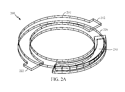
[0029] Figures 2A and 2B illustrate an exemplary inductor 200 in accordance
with some
examples of the disclosure. As shown in Figure 2A, the inductor 200 may
include a first
curved metal plate 210 (e.g., a "top" metal layer, also referred to as a
"trace"), a second
curved metal plate 220 (e.g., a "bottom" metal layer, also referred to as a
"trace")
substantially co-located below and parallel to the first curved metal plate
210, and an
elongated via 230 between the first curved metal plate 210 and the second
curved metal
plate 220. The elongated via 230 conductively couples the first curved metal
plate 210
to the second curved metal plate 220 through an insulating layer (not shown in
Figure
2A). The first curved metal plate 210 may include a first terminal 212 at one
end, and
the second curved metal plate 220 may include a second terminal 222 at one
end. The
first terminal 212 and the second terminal 222 may be configured to connect to
external
components for input and output of current through the inductor 200.
[0030] Figure 2B shows a side view 200A and a top view 200B of the inductor
200. As shown
in Figure 2B, an induced current 232 may traverse the inductor 200 from the
first curved
metal plate 210 through the elongated via 230 to the second curved metal plate
220 and
vice versa. The elongated via 230 may be drilled or cut through an insulating
layer 240
of a coreless substrate of a semiconductor device. The first curved metal
plate 210 may
be on "top" of the insulating layer 240 and the second curved metal plate 220
may be on
the "bottom" of the insulating layer 240.
[0031] As illustrated in Figures 2A and 2B, the elongated via 230 may
substantially follow the
curve of and be narrower than the first curved metal plate 210 and the second
curved
metal plate 220. The elongated via 230 may provide a longer and flatter
transition
between the first curved metal plate 210 and the second curved metal plate 220
for the
induced current 232. The elongated via 230 may have an aspect ratio of width-
to-height
of approximately 2-to-1 (2:1) or larger. As shown in Figure 2B, the "width"
(also
referred to as the "length") of the elongated via 230 is the dimension of the
elongated
CA 02999507 2018-03-21
WO 2017/065960
PCT/US2016/053620
7
via 230 along the curve (substantially parallel to the inside and outside
edges) of the
first and second curved metal plates 210 and 220. The "height" of the
elongated via 230
is the dimension of the elongated via 230 between the first and second curved
metal
plates 210 and 220. The depth of the elongated via 230 is the dimension of the
elongated via 230 between (substantially perpendicular to) the inside and
outside edges
of the first and second curved metal plates 210 and 220.
[0032] Thus, unlike the induced current 132 having to make a high-resistance
90 degree bend
to traverse the via 130 from the first curved metal plate 110 to the second
curved metal
plate 120, as in the inductor 100, the induced current 232 follows a longer,
flatter, and
therefore lower resistance path as it traverses the elongated via 230 from the
first curved
metal plate 210 and through to the second curved metal plate 220. As an
example,
where the thickness of the insulating layer 240 is approximately 401,tm, the
height of the
elongated via 230 may be approximately 401,tm and the width of the elongated
via 230
may be approximately 801,tm.
[0033] Note that although Figures 2A and 2B illustrate the inductor 200 as
having a circular
shape, it will be appreciated that the inductor 200 may have other shapes,
such as an
octagonal shape.
[0034] The insulating layer 240 may be one or more layers of silicon dioxide
(Si02), silicon
nitride (Si3N4), silicon oxynitride (SiON), tantalum pentoxide (Ta205),
aluminum
oxide (A1203), hafnium oxide (Hf02), benzocyclobutene (BCB), polyimide (PI),
polybenzoxazoles (PBO), or other material having similar insulating and
structural
properties, as is known in the art. The first curved metal plate 210, the
second curved
metal plate 220, and the elongated via 230 may be one or more layers of
aluminum (Al),
copper (Cu), tin (Sn), nickel (Ni), gold (Au), silver (Ag), or other suitable
electrically
conductive material, as is known in the art.
[0035] The configuration of the inductor 200 results in a lower DC resistance
and a higher Q-
factor for the inductor 200. For example, the Q-factor of the inductor 200 may
be 131.6
at 1GHz, whereas the Q-factor of the inductor 100 may be 122.7 at 1GHz. The
configuration of the inductor 200 may further result in a high-performance RF
inductor
implementation that improves PA performance by reducing loss in the inductor
200 by
approximately 7.25%, or as much as 10%, with no manufacturing process change
and
minimal area increase on the insulating layer 240 (e.g., 2.3%).
CA 02999507 2018-03-21
WO 2017/065960
PCT/US2016/053620
8
[0036] Figure 3 illustrates an exemplary conventional spiral inductor 300. As
shown in Figure
3, the spiral inductor 300 may include a spiral metal plate 310. The spiral
metal plate
310 may include a first terminal 312 at one end conductively coupled to an
interconnect
320 and a second terminal 322 at the other end. The first terminal 312, via
the
interconnect 320, and the second terminal 322 may be configured to connect to
external
components for input and output of current through the spiral inductor 300.
For
example, a current may enter the spiral inductor 300 at the first terminal 312
via the
interconnect 320, travel along the spiral metal plate 310, and exit the spiral
inductor 300
at the second terminal 322. Alternatively, current may travel the same path in
the
opposite direction.
[0037] Figure 4 illustrates an exemplary stacked co-spiral inductor 400 in
accordance with
some examples of the disclosure. As shown in Figure 4, the stacked co-spiral
inductor
400 may include a first curved metal plate 410, a second curved metal plate
420
substantially co-located below the first curved metal plate 410, and a third
curved metal
plate 430 co-located between the first curved metal plate 410 and the second
curved
metal plate 420. As illustrated in Figure 4, each of the first curved metal
plate 410, the
second curved metal plate 420, and the third curved metal plate 430 may
consist of
multiple layers of metal. For example, each curved metal layer may consist of
top and
bottom metal layers connected by a middle metal layer.
[0038] The third curved metal plate 430 may be configured to conductively
couple the first
curved metal plate 410 to the second curved metal plate 420. The first curved
metal
plate 410 may include a first terminal 412 at one end and a first via 414 at
the other end.
The second curved metal plate 420 may include a second terminal 422 at one end
and a
second via 424 at the other end. The first terminal 412 and the second
terminal 422 may
be configured to connect to external components for input and output of
current through
the stacked co-spiral inductor 400.
[0039] The first via 414 may be configured to directly couple the first curved
metal plate 410 to
the third curved metal plate 430. The second via 424 may be configured to
directly
couple the second curved metal plate 420 to the third curved metal plate 430.
For
example, a current may enter the stacked co-spiral inductor 400 at the first
terminal 412,
travel along the first curved metal plate 410 to the first via 414, then from
the first via
414 through the third curved metal plate 430 to the second via 424, and from
the second
via 424 through the second curved metal plate 420 to the second terminal 422
to exit the
CA 02999507 2018-03-21
WO 2017/065960
PCT/US2016/053620
9
stacked co-spiral inductor 400. Alternatively, the current may travel the same
path in
the opposite direction.
[0040] Note that although the first via 414 and the second via 424 are
illustrated as cylindrical
vias, similar to the via 130, it will be appreciated that the first via 414
and the second
via 424 may be elongated vias, similar to the elongated via 230, and may
provide the
same advantages.
[0041] The presence of the third curved metal plate 430 may provide better
(i.e., lower) DC
resistance and thermal conductivity along with lower inductor power loss
compared to a
conventional spiral inductor, such as the spiral inductor 300. For example,
the
configuration of the stacked co-spiral inductor 400 may provide a 60% lower
power loss
than a conventional single layer spiral inductor (e.g., spiral inductor 300).
When
integrated with a coreless substrate, the stacked co-spiral inductor 400 may
also reduce
external components, cost, and area on the substrate. For example, the stacked
co-spiral
inductor 400 may take up an area of 1.41mm2 on the substrate compared to an
area of
1.69mm2 for the spiral inductor 300. The DC resistance of the stacked co-
spiral
inductor 400 may be approximately 23.1mOhm for 7 nanoHenries (nH), while the
DC
resistance of the spiral inductor 300 may be approximately 67.4mOhm for 7nH.
The
power loss at 2Amps for the stacked co-spiral inductor 400 may be
approximately
92.3mW compared to approximately 270mW for the spiral inductor 300. Finally,
the
RF resistance for the stacked co-spiral inductor 400 may be a Q-factor of
approximately
103 at 1GHz with 7nH compared to a Q-factor of approximately 101 at 1GHz with
7nH
for the spiral inductor 300.
[0042] The substrate may be one or more layers of silicon dioxide (Si02),
silicon nitride
(Si3N4), silicon oxynitride (SiON), tantalum pentoxide (Ta205), aluminum oxide
(A1203), hafnium oxide (Hf02), benzocyclobutene (BCB), polyimide (PI),
polybenzoxazoles (PBO), or other material having similar insulating and
structural
properties, as is known in the art. The first curved metal plate 410, the
second curved
metal plate 420, the third curved metal plate 430, the first via 414, and the
second via
424 may be one or more layers of aluminum (Al), copper (Cu), tin (Sn), nickel
(Ni),
gold (Au), silver (Ag), or other suitable electrically conductive material, as
is known in
the art.
[0043] Note that as used herein, the terms "substantially" and "approximately"
are not relative
terms of degree, but rather, reflect the reality that, due to tolerances in
manufacturing
CA 02999507 2018-03-21
WO 2017/065960
PCT/US2016/053620
processes, two components may not be exactly the same size or have an exact
orientation with respect to each other, or that a given component may not be
an exact
size. Rather, the terms "substantially" and "approximately" mean that the
size,
orientation, etc. of the component(s) need only be within some tolerance
threshold of
the described size, orientation, etc. Thus, for example, when one component is
described as being "substantially" above or below another component, it means
that the
components are aligned vertically within some tolerance threshold. Similarly,
as
another example, when one component is described as being "approximately" a
given
size, it means that the component is within a given tolerance threshold of the
given size.
The tolerance threshold may be determined by the capabilities of the
manufacturing
process, the requirements of the device and/or components being manufactured,
and the
like.
[0044] It will be appreciated that even if the terms "substantially" or
"approximately" are not
used to describe a size, orientation, etc. of component(s), it does not mean
that the size,
orientation, etc. of the component(s) must be exactly the described size,
orientation, etc.
Rather, the described size, orientation, etc. need only be within some
tolerance threshold
of the described size, orientation, etc.
[0045] Figure 5 illustrates an exemplary power amplification (PA) circuit 500
with multiple
inductors in accordance with some examples of the disclosure. As shown in
Figure 5,
the PA circuit 500 may include a ground 510, a power supply 520, a first
inductor 530
(e.g., inductor 200 or stacked co-spiral inductor 400) coupled to the power
supply 520,
an input 540, such as an antenna input, coupled between the first inductor 530
and the
ground 510 that gates the PA circuit 500, a bandpass filter 550 coupled
between the first
inductor 530 and the input 540, an RF resistive load 560 coupled between the
bandpass
filter 550 and the ground 510, and an output tap 570 across the RF resistive
load 560.
The bandpass filter 550 may include one or more inductors (e.g., inductor 200
or
stacked co-spiral inductor 400) and acoustic filters.
[0046] In this description, certain terminology is used to describe certain
features. The term
"mobile device" can describe, and is not limited to, a music player, a video
player, an
entertainment unit, a navigation device, a communications device, a mobile
device, a
mobile phone, a smartphone, a personal digital assistant, a fixed location
terminal, a
tablet computer, a computer, a wearable device, a laptop computer, a server,
an
automotive device in an automotive vehicle, and/or other types of portable
electronic
CA 02999507 2018-03-21
WO 2017/065960
PCT/US2016/053620
11
devices typically carried by a person and/or having communication capabilities
(e.g.,
wireless, cellular, infrared, short-range radio, etc.). Further, the terms
"user equipment"
(UE), "mobile terminal," "mobile device," and "wireless device," can be
interchangeable.
[0047] Inductors and circuits according to the examples above (e.g., the
inductor 200, the
stacked co-spiral inductor 400, and the PA circuit 500) can be used for a
number of
different applications, such as in the circuit components of a mobile device.
Referring to
Figure 6 as an example, a user equipment (UE) 600 (here a wireless device) has
a
platform 602 that can receive and execute software applications, data, and/or
commands
transmitted from a radio access network (RAN) that may ultimately come from a
core
network, the Internet, and/or other remote servers and networks. Platform 602
can
include inductors and PA circuits as well as a transceiver 606 operably
coupled to an
application specific integrated circuit (ASIC) 608, or other processor,
microprocessor,
logic circuit, or other data processing device. The ASIC 608 or other
processor executes
the application programming interface (API) 610 layer that interfaces with any
resident
programs in a memory 612 of the UE 600. Memory 612 can be comprised of read-
only
memory (ROM) or random-access memory (RAM), electrically erasable programmable
ROM (EEPROM), flash cards, or any memory common to computer platforms.
Platform 602 can also include a local database 614 that can hold applications
not
actively used in memory 612. Local database 614 is typically a flash memory
cell, but
can be any secondary storage device as known in the art, such as magnetic
media,
EEPROM, optical media, tape, soft or hard disk, or the like. Platform 602
components
can also be operably coupled to external devices such as antenna 622, display
624,
push-to-talk button 628, and keypad 626 among other components, as is known in
the
art.
[0048] The wireless communication between UE 600 and the RAN can be based on
different
technologies, such as code division multiple access (CDMA), wideband CDMA (W-
CDMA), time division multiple access (TDMA), frequency division multiple
access
(FDMA), Orthogonal Frequency Division Multiplexing (OFDM), Global System for
Mobile Communications (GSM), 3GPP Long Term Evolution (LTE), or other
protocols
that may be used in a wireless communications network or a data communications
network.
CA 02999507 2018-03-21
WO 2017/065960
PCT/US2016/053620
12
[0049] Figure 7 illustrates an exemplary flow 700 for forming an inductor
device, such as
inductor 200, in accordance with some examples of the disclosure. The flow
illustrated
in FIG. 7 may be performed during a manufacturing process of the inductor
device. In
an embodiment, the inductor device may be one of an RF front end module, a
filter, or a
PA. The inductor device may be incorporated into a device selected from a
group
comprising a music player, a video player, an entertainment unit, a navigation
device, a
communications device, a mobile device, a mobile phone, a smartphone, a
personal
digital assistant, a fixed location terminal, a tablet computer, a computer, a
wearable
device, a laptop computer, a server, an automotive device in an automotive
vehicle, an
RF front end module, a filter, or a PA.
[0050] At 702, the flow 700 includes forming a first curved metal plate, such
as first curved
metal plate 210 in Figures 2A and 2B. At 704, the flow 700 includes forming a
second
curved metal plate, such as second curved metal plate 220 in Figures 2A and
2B, below
and substantially vertically aligned with the first curved metal plate. In an
embodiment,
the first curved metal plate and the second curved metal plate may be octagon
shaped.
The first curved metal plate and the second curved metal plate may have
approximately
a same length.
[0051] At 706, the flow 700 includes forming a first elongated via, such as
elongated via 230 in
Figures 2A and 2B, vertically aligned between the first curved metal plate and
the
second curved metal plate. The first elongated via may be configured to
conductively
couple the first curved metal plate to the second curved metal plate and may
have an
aspect ratio of a width to a height of the first elongated via of at least
approximately 2 to
1. The first elongated via may be completely within a vertical perimeter
defined by an
inside edge and an outside edge of the first curved metal plate.
[0052] At 708, the flow 700 may optionally include providing a coreless
substrate, such as
insulating layer 240 in Figure 2B, between the first curved metal plate and
the second
curved metal plate.
[0053] At 710, the flow 700 may optionally include forming a third curved
metal plate, such as
the third curved metal plate 430 in Figure 4, below and substantially
vertically aligned
with the second curved metal plate.
[0054] At 712, the flow 700 may optionally include forming a second elongated
via, such as
the second via 424 in Figure 4, vertically aligned between the second curved
metal plate
and the third curved metal plate. The second elongated via may be configured
to
CA 02999507 2018-03-21
WO 2017/065960
PCT/US2016/053620
13
conductively couple the second curved metal plate to the third curved metal
plate and
may have an aspect ratio of a width to a height of at least approximately 2 to
1.
[0055] Although FIG. 7 illustrates a particular order of operations, it will
be appreciated that
the operations may be performed in a different order, depending on the
manufacturing
process being used to form the inductor device.
[0056] The terminology used herein is for the purpose of describing particular
examples only
and is not intended to be limiting of examples of the disclosure. As used
herein, the
singular forms "a," "an," and "the" are intended to include the plural forms
as well,
unless the context clearly indicates otherwise. It will be further understood
that the
terms "comprises," "comprising," "includes," and/or "including," when used
herein,
specify the presence of stated features, integers, actions, operations,
elements, and/or
components, but do not preclude the presence or addition of one or more other
features,
integers, actions, operations, elements, components, and/or groups thereof
[0057] It should be noted that the terms "connected," "coupled," or any
variant thereof, mean
any connection or coupling, either direct or indirect, between elements, and
can
encompass a presence of an intermediate element between two elements that are
"connected" or "coupled" together via the intermediate element.
[0058] Any reference herein to an element using a designation such as "first,"
"second," and so
forth does not limit the quantity and/or order of those elements. Rather,
these
designations are used as a convenient method of distinguishing between two or
more
elements and/or instances of an element. Thus, a reference to first and second
elements
does not mean that only two elements can be employed, or that the first
element must
necessarily precede the second element. Also, unless stated otherwise, a set
of elements
can comprise one or more elements.
[0059] Nothing stated or illustrated in this application is intended to
dedicate any component,
action, feature, benefit, advantage, or equivalent to the public, regardless
of whether the
component, action, feature, benefit, advantage, or the equivalent is recited
in the claims.
[0060] Although some aspects have been described in connection with a device,
it goes without
saying that these aspects also constitute a description of the corresponding
method, and
so a block or a component of a device should also be understood as a
corresponding
method action or as a feature of a method action. Analogously thereto, aspects
described
in connection with or as a method action also constitute a description of a
corresponding
block, detail, or feature of a corresponding device. Some or all of the method
actions
CA 02999507 2018-03-21
WO 2017/065960
PCT/US2016/053620
14
can be performed by a hardware apparatus (or using a hardware apparatus), such
as, for
example, a microprocessor, a programmable computer or an electronic circuit.
In some
examples, some or a plurality of the most important method actions can be
performed
by such an apparatus.
[0061] In the detailed description above it can be seen that different
features are grouped
together in examples. This manner of disclosure should not be understood as an
intention that the claimed examples require more features than are explicitly
mentioned
in the respective claim. Rather, the situation is such that inventive content
may reside in
fewer than all features of an individual example disclosed. Therefore, the
following
claims should hereby be deemed to be incorporated in the description, wherein
each
claim by itself can stand as a separate example. Although each claim by itself
can stand
as a separate example, it should be noted that-although a dependent claim can
refer in
the claims to a specific combination with one or a plurality of claims-other
examples
can also encompass or include a combination of said dependent claim with the
subject
matter of any other dependent claim or a combination of any feature with other
dependent and independent claims. Such combinations are proposed herein,
unless it is
explicitly expressed that a specific combination is not intended. Furthermore,
it is also
intended that features of a claim can be included in any other independent
claim, even if
said claim is not directly dependent on the independent claim.
[0062] It should furthermore be noted that methods disclosed in the
description or in the claims
can be implemented by a device comprising means for performing the respective
actions
of this method.
[0063] Furthermore, in some examples, an individual action can be subdivided
into a plurality
of sub-actions or contain a plurality of sub-actions. Such sub-actions can be
contained in
the disclosure of the individual action and be part of the disclosure of the
individual
action.
[0064] While the foregoing disclosure shows illustrative examples of the
disclosure, it should
be noted that various changes and modifications could be made herein without
departing
from the scope of the disclosure as defined by the appended claims. The
functions
and/or actions of the method claims in accordance with the examples of the
disclosure
described herein need not be performed in any particular order. Additionally,
well-
known elements will not be described in detail or may be omitted so as to not
obscure
the relevant details of the aspects and examples disclosed herein.
Furthermore, although
CA 02999507 2018-03-21
WO 2017/065960
PCT/US2016/053620
elements of the disclosure may be described or claimed in the singular, the
plural is
contemplated unless limitation to the singular is explicitly stated.