Note: Descriptions are shown in the official language in which they were submitted.
CA 03002412 2018-04-18
1
Description
Power distributor
The invention relates to a modular power distributor intended for direct
mounting on a
supporting rail, comprising a number of power distribution modules, in
particular in the form of
modular devices. The invention further relates to a method for operating such
a power
distributor.
Below, a power distributor is particularly understood as an electrical
installation having one or
more electric load circuits to which a current is supplied from a main line.
In the context of the
power distributor, safety mechanisms are provided which secure each load
circuit against
overload or a short circuit.
The safety mechanisms are in particular mechanical, electronic or mechatronic
circuit breakers,
which are connected between a main circuit or a supply and the load circuits.
The circuit
breakers are often single-wired by flexible wires to the power supply and
load. Thus, the
assembly of such a power distributor is particularly labor intensive.
Furthermore, the switching
system formed by such a power distributor is relatively hard to navigate due
to the single wiring,
which makes repair and subsequent changes in the assembled state of the power
distributor
disadvantageous.
To reduce the wiring costs of conventional power distributors, so-called
modular power
distributors can be used. Such power distributors are composed of a plurality
of
individual power distribution modules which are electrically conductive and
can be
coupled with each other. The power distribution modules are typically mounted
directly
side by side as modular devices on a supporting rail (DIN rail) and have on
the one
hand supply terminals for feed-in and for the load and on the other hand, at
least one
socket-like slot for the interposition of a circuit breaker. The lined-up
modules are
typically electrically conductively coupled in a visually clear manner by
means of a
conductor rail, which bridges a plurality of modules.
2
In the context of such a power distributor, such power distribution modules
equipped
with breakers are in particular provided at the junctions where the load
circuits branch
off from the main power line. The circuit breakers are used here ii needed to
separate
the respective, associated load circuit from the live main power line.
Typically, wirings for signaling are provided by a series of individual power
distribution modules. The circuit breakers used for this purpose have
integrated signal
contacts (NO and NC), which, depending on whether they are applied in the
context of
a single or group signaling, can be wired and actuated by a switching signal.
When using serial communication and signaling methods, a so-called daisy-chain
arrangement may be formed by wiring the power distribution modules. In this
case, in
terms of use it is desirable in a bus functionality that each circuit breaker
or each power
distribution module is assigned a separate signal or device address, so that
each circuit
breaker as part of a signal bus can be individually addressed, or in
particular
controlled. Particularly with regard to the modular design of the power
distributor, it
may further be desirable that the address allocation also takes into account
empty slots
in the modules, so that when a circuit breaker is inserted subsequently, no
new address
must be assigned.
In case of failure, that is, particularly in a galvanic interruption of the
daisy-chain
arrangement, it is particularly desirable to locate the defective circuit
breaker and / or
the defective power distribution module or the point of interruption in the
series
connection as quickly as possible.
An object of the invention is to provide a power distributor which is
particularly
suitable in terms of a communication and / or signaling application.
Furthermore, a
method for operating such a power distributor is to be provided.
The aforementioned object may be achieved by a power distributor and a method
for
operating a power distributor according to the invention.
CA 3002412 2019-06-10
3
The power distributor according to the invention is designed to be modular
with a
number of attached or attachable connection modules - hereinafter shortened to
modules. The individual modules and thus the power distributor are adapted and
arranged for direct mounting on a supporting rail, such as a DIN or G-rail.
For this
purpose, the modules can be mounted on the supporting rail, in particular in
the manner
of modular devices in a row next to each other. The module package thus formed
is
connected to a common first controller (that is, to a common first control
device).
The modules each have a number of lateral coupling contacts for an electrical
and / or
signaling contact connection with at least one further module attached or
attachable to
the side of the respective module. Inside the module, in each case one base
resistor is
connected such between two contacts, that the base resistors of the lined-up
modules
form a series-connected resistor chain in the interconnection of the module
package.
The modules are used in particular for power distribution or for branching a
load
circuit, which is coupled by means of a supply line, and 'are each equipped
with or can
be equipped with an actuatable circuit breaker. The circuit breaker interrupts
the
respectively connected load circuit automatically in the event of an overload
or short-
circuit.
The circuit breakers each have a breaker-internal second controller (that is,
a second
control unit), which - in particular in addition to other functions ¨ serves
at least also
for recording a drop in voltage at the respectively associated base resistor.
On the basis
of the recorded voltage, the second controllers transmit a controller signal
to the first
controller, wherein said first controller includes a DC power source to supply
and
energize the resistor chain.
Thus, a power distributor is provided which is particularly suitable in terms
of a
communication and / or signaling application. By means of the resistor chain,
the
modules are serially connected to the first controller in the manner of a
daisy-chain
CA 3002412 2019-06-10
CA 03002412 2018-04-18
S. 4
arrangement. Due to the module-internal resistor chain, the contact link is
not
interrupted even in a module that is not equipped with a circuit breaker.
Furthermore,
the contact connection between the modules results in a power distributor with
particularly low wiring and circuitry costs.
The modules each comprise a preferably flat (module) housing made of an
electrically
insulating material. The modules are advantageously coupled in a preferred
mounting
position with a main power supply or a feed for power distribution or
branching.
Preferably, each module housing has a socket-like slot on the housing front
side, i.e. on
the side facing away from the supporting rail, for plugging the circuit
breaker. By
means of the circuit breaker, the connected load circuit can be galvanically
interrupted
or separated. The plug connection between the module and the circuit breaker
is made,
for example, via multilam plugs, pin plugs, or preferably flat plugs.
The modular design of the power distributor allows for a high degree of
prefabrication
and thereby comparatively low manufacturing and assembly costs. In particular,
it is
possible to particularly easily adapt a power distributor by means of a series
of a
corresponding number of modules to a desired number of load circuits that are
to be
connected. Thus, the power distributor can be particularly flexibly used in an
electrical
system.
The circuit breaker is typically designed as a mechanical, electronic or
mechatronic
switch or a relay, and typically has a supply terminal through which a network-
side,
and thus current-carrying, power cable is connected by a first plug contact
with the
module, and a load connection, via which the load-side, outgoing power line is
connected by a second plug contact with the module.
The circuit breakers are attached or can be fitted to the power distributor in
the grid
dimension predetermined by the modules. The modules are in particular
approximately
as wide as a circuit breaker, that is, a module preferably serves for
receiving a
respective circuit breaker. Preferably, it is hereby possible to operate the
equipped
CA 03002412 2018-04-18
circuit breaker of the power distributor both in a series circuit and in a
parallel circuit,
wherein optional additional connections are provided on the modules for this
purpose.
As part of their design as modular devices, the modules preferably have a
profiled slot
(snap-in groove) on the rear of the housing for mounting the module package to
the
supporting rail. In the intended mounting position of the modules, the housing
front
side faces a user. The profile direction of the housing (and of the rail
corresponding
thereto) defines a row direction along which a plurality of modules can be
aligned as
intended next to one another in the assembled state. The housing sides
oriented
perpendicular to this row direction are hereinafter referred to as (housing)
end faces.
The first controller is preferably adapted and configured as an external
control unit for
the purposes of a higher-level control device, a remotely controlled actuation
of the
circuit breakers and / or a recording of measured values as well as diagnosis
in case of
failure. In the scope of the invention it is also conceivably advantageous,
for example,
that the first controller is attached to the connection modules as a control
module which
is part of the module package.
The second controller of the circuit breaker is furthermore particularly
suitable for
actuating the circuit breaker in response to a switching signal of the first
controller. For
this purpose, the circuit breaker preferably has two signal contacts (NC, NO)
for
connection to the module that are interconnected with the second
controller. Furthermore, the circuit breaker comprises at least one
communication
contact for connection to a communication line, in particular as part of a bus
connection
for signal contact functions.
In a preferred embodiment, a communication line formed by the coupling
contacts is
provided for guiding the controller signals. The communication line is thus a
substantially module-internal wiring of the modules or of the second
controllers of the
circuit breakers equipped therewith, for the purposes of signaling and / or
actuating the
circuit breaker with the first controller. By means of the coupling contacts,
a cross
wiring of the modules to each other is provided, wherein in the assembled
state, the
CA 03002412 2018-04-18
6
coupling contacts realize an electrically conductive connection in the row
direction, that
is, from housing end face to housing end face, between any two adjacent
modules.
The communication line is also used for guiding a data bus signal (for
example, the
switching signal) from the first controller to one or more second controllers,
wherein
the resistor chain in particular serves as a second communication line for
guiding an
address bus signal. This makes it possible, for example, to switch the circuit
breakers of
different load circuits remotely, to reset them, to monitor them or to
parameterize them.
Parameterization in this context is understood to be the setting of, for
example, tripping
limits and control or operating parameters, such as the rated current of the
relevant
circuit breaker. For this purpose, the data bus signals are transmitted from
the first
controller to the second controller of the respective circuit breaker, which
is adapted
and configured to process and implement such signals.
In an advantageous embodiment, the connection module has a contact opening
with a
split plug base contact, into which a plug contact of the circuit breaker can
be inserted.
The base resistor is connected between the thus formed partial plug base
contacts. The
plug contact preferably designed as a flat plug hereby expediently has a split
plug tab as
partial plug contacts. Thereby, the respective second controller is connected
in a
structurally simple and cost effective way for recording the voltage dropped
across the
base resistor.
In a suitable embodiment, the connection module has a ground connection, which
is
contacted or can be contacted on the one hand to the respective second
controller and
on the other hand, to a partial plug contact of the plug contact. A switching
element
actuatable by the second controller is connected between the ground connection
and the
partial plug contact. The switching element is preferably integrated in the
respective
circuit breaker and is designed, for example, as a transistor. By operating
the switching
element, it is thus possible to switch the resistor chain to ground or
reference potential
on the (row) position of the partial plug contacts.
CA 03002412 2018-04-18
7
In the inventive method for operating the power distributor, the first
controller
determines a total resistance value of the resistor chain. Using this total
value,
subsequently a number value corresponding to the number of connected modules
is
determined by the first controller. For this purpose, the resistor chain is
conveniently
connected at one end to the DC power source of the first controller, and at
the other end
to ground (reference potential). This way, the same electric current flows
through all
the base resistors so that the number of the connected modules is directly
determined
from the known resistance values of the base resistors and of the total
resistance
value. The total resistance value is determined in a simple manner by the
output voltage
of the DC power source.
In a preferred development of the method, module-specific device addresses are
sent to
the connected second controllers in response to the controller signals of the
connected
second controllers. The second controllers record the falling voltage at the
respective
base resistor by means of the partial plug contacts. The recorded voltage
value is sent as
a controller signal to the first controller. The device address is determined,
for example,
as an integer (rounded) quotient of the voltage value and the voltage drop of
a single
base resistor. This way, each second controller receives a (physical) device
address
which decreases along the resistor chain, starting from the DC power source.
The
device addresses are therefore not assigned based on the number of connected
circuit
breakers, but instead based on the number of connected modules or connected
base
resistors.
In other words, with N connected modules, the first device address is assigned
to the
second controller in module N (i.e., with respect to the DC power source, at
the end of
the resistor chain, opposite the DC power source), the second device address
is
associated with the second controller in the module N-1, and so forth, wherein
the
second controller in the first module (i.e., the module on the first base
resistor of the
resistor chain) is the N-th address. This way, simple addressing of the second
controller
is made possible. In particular, it also makes it possible in view of empty
module plug
slots to allocate addresses, so that if a module is subsequently equipped with
a circuit
CA 03002412 2018-04-18
8
breaker, no new address needs to be assigned and the second controllers
continue to
operate with the already assigned device addresses.
During addressing, the first controller drives a current (addressing current)
as an
address bus signal through the resistor chain of the module package by means
of the
direct current source. In a suitable embodiment, the base resistors, for
example, each
have a resistance value of 1 k52, so that with a generated addressing current
of 1 mA, a
voltage of 1V is dropped at each base resistor. The respective voltage value
of the
module is in this case suitably measured by the respective second controller,
on the
base resistor side facing the DC power source side.
During addressing, the second controller primarily connected downstream of the
common first controller records the highest voltage value and transmits it as
a controller
signal to the first controller via the communication line. The subsequent
circuit breaker
in the series arrangement, or the second controller thereof, thus records a
voltage value
decreased by 1 V and reports it to the first controller. In this manner, a
voltage value
and a device address therefrom are assigned to each connected controller.
In a particularly user-friendly development, the module-specific device
addresses of the
second controller are converted as a function of the number value into a set
of logical
addresses which correspond to the row order of the lined-up connection
modules. This
way, the sequence of the N device addresses is effectively reversed so that
the first
logical address is assigned to the second controller in the first module
behind the DC
power source, the second logical address is assigned to the second controller
in the next
module, etc. Thus, the user is ensured a particularly intuitive operation of
the power
distributor.
In an advantageous embodiment of the method, in a galvanic interruption of the
resistor
chain, a search process is initiated or triggered to determine the position of
the
interruption. Due to the interruption, the DC power source is no longer
connected to
ground (reference potential) via the resistor chain (i.e., separated
therefrom) so that no
address current flows through the resistor chain. On the one hand, the first
controller is
CA 03002412 2018-04-18
9
arranged in a simple manner to record such an interruption by detecting the
address
current. Furthermore, the connected second controllers record only a voltage
drop of 0
V at all positions, so that an interruption is additionally or alternatively
signaled by the
controller signals to the first controller.
This way, wire breaks or defective components in the module package are
detected
easily and reliably. The determined position is then advantageously made
available to
or signaled to a user. This simplifies maintenance or repair of the power
distributor. In
order to ensure a successful search process, preferably all modules of the
module
package are provided with a respective circuit breaker for this application.
In a suitable embodiment, at the beginning of the search process, all
connected second
controllers are set to an ON state in which the respective switching element
is closed.
Thereby, the base resistors provided with a circuit breaker are in particular
connected to
the respective ground connection of the module. As a result, all the base
resistors are
connected to ground on the side facing away from the DC power source, and the
address current flows from the DC power source to ground.
In an expedient development, new addressing is started during the search
process. For
this purpose, the number value for the number of the connected modules is
determined
by the first controller, and device addresses are distributed to the
respective second
controllers. The second controller with the first device address is then
switched off. In a
preferred embodiment, the search process is terminated when there is no second
controller with the first device address. This way, the first controller is
able to
determine the point of interruption within the module package.
After all the switching elements of the circuit breakers have been set to the
ON state at
the beginning of the search process, and the respective side of the base
resistor is
connected to ground, a voltage (of, for example, again 1 V) drops at all base
resistors
located between the DC power source and the point of interruption. If the
interruption is
downstream of the first module or downstream of the first base resistor, the
second
controller associated with the first module notifies the first device address.
Then the
CA 03002412 2018-04-18
switching element of said second controller is turned off, that is, the base
resistor is
disconnected from the ground connection. As a result, the second controller
connected
next in the series reports via its base resistor. Then, the switching element
thereof is
also turned off. This (search) process is continued until no second controller
with the
first device address reports. Thereby, the point of interruption between the
final
detected second controller, and the module connected thereto and not detected,
is
determined by the first controller.
The first controller and the second controllers of the power distributor
according to the
invention are in this case generally configured ¨ programmatically and / or in
terms of
circuit technology - for performing the inventive method described above.
The controllers are essentially each formed at least by a microcontroller
having a
processor and a data memory in which the functionality for performing the
method
according to the invention in terms of an operating software (firmware) is
programmatically implemented, so that the method - possibly in interaction
with a user
- is performed automatically upon implementing the operating software in the
microcontroller.
In a possible embodiment within the scope of the invention, alternatively the
first
controller and / or the second controllers are however formed by programmable
electronic components, for example, an application-specific integrated circuit
(ASIC) in
which the functionality for performing the method according to the invention
is
implemented with circuitry means.
Below, embodiments of the invention are explained in detail with reference to
a
drawing. These drawings show, in simplified and schematic representations:
FIG. 1 a perspective view of a power distributor with a supply module,
with a
signal module, with six intermediate connection modules, and with two
equipped circuit breakers,
FIG. 2 a perspective view of a connection module,
CA 03002412 2018-04-18
11
FIG. 3 a perspective view of a connection module without a housing,
FIG. 4 a side view of the connection module without a housing,
FIG. 5 a perspective view of a plurality of contact elements of the
connection
module,
FIG. 6 a perspective view with a view of a rear panel of the contact
elements
with an intermediate base resistor,
FIG. 7 a schematic circuit of the power distributor with a controller and
N
connection modules connected thereto, each having an equipped circuit
breaker, and
FIG. 8 a flowchart for a search process of the first controller during
failure
diagnosis.
Corresponding parts and variables are always provided in all figures with the
same
reference numerals.
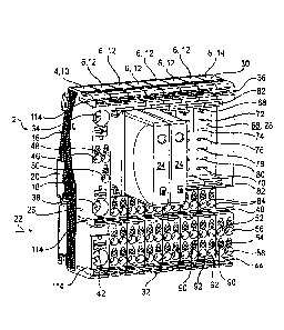
As (power distribution) modules, the power distributor 2 shown in FIG. 1
comprises a
supply module 4, six connection modules 6 and a signal module 8, wherein the
connection modules 6 are shown individually in FIG. 2. Each module 4, 6, 8
includes a
housing 10, 12 or 14 that is separate, i.e., separated from the other modules
4, 6, 8.
Each module 4, 6, 8 is designed in the form of a modular device and
accordingly has a
groove-like slot 18 on the rear panel of a housing 16, with which the
respective module
4, 6, 8 can be snapped onto a supporting rail 20 for assembly.
The profile direction of this slot 18 - and, accordingly, also the profile
direction of the
supporting rail 20 corresponding to this slot 18 in the assembled state -
define a row
direction 22 along which the modules 4, 6, 8 are lined up together. In the
exemplary
embodiment shown in FIG. 1, two circuit breakers 24 are arranged at a
respective
connection module 6, inside the (module) package formed of the modules 4, 6,
8,
CA 03002412 2018-04-18
12
wherein the supply module 4 on the one hand and the signal module 8 on the
other hand
externally flank the connection modules 6 in the row direction 22 as side
parts.
The housing surfaces of each module 4, 6, 8 situated opposite each other in
the row
direction 22 are referred to as the (housing) end face 26 of the respective
module 4, 6,
8. The housing side of each module 4, 6, 8 situated opposite to the rear panel
16 is
referred to as the (housing) front side 28 of the module 4, 6, 8. This front
side 28 faces
a user when the power distributor 2 is mounted in a switch cabinet. The two
remaining
housing sides of each module 4, 6, 8 are - according to the conventional
assembly
position of the module 4, 6, 8 ¨ referred to as the (housing) top 30 and the
(housing)
bottom 32, independent of the actual position in the surrounding space.
The supply module 4 comprises a supply terminal 34 for making electrical
contact to a
non-illustrated main circuit and thus for feeding an electric current into the
power
distributor 2. The supply terminal 34 is arranged on the front side 28 of the
housing 10
near the top 30, and is configured as a connecting terminal for a wire or
stranded
conductor of the main circuit. Within the housing, the supply terminal 34 is
coupled in
an electrically conductive manner to a not-shown coupling contact which is
disposed
within a groove-like housing slot 36.
At approximately half the height of the housing 10, the supply module 4 has a
ground
connection 38 as a negative terminal (DC power) or as a neutral conductor
(AC). Within the housing 10, the ground connection 38 is coupled in an
electrically
conductive manner with a lateral socket for a contact connection to the
attached
connection module 6, and to a coupling contact which is positioned in a
housing slot 40
at the front side 28 inserted centrally at the housing 10.
The supply module 4 further comprises a return port 42 for making electrical
contact to
a non-illustrated current return as part of a protective or functional ground.
The return
port 42 is located near the bottom 32 at the front side 28 of the housing 10,
and like the
supply terminal 34 and the ground connection 38, is designed as a connecting
CA 03002412 2018-04-18
13
terminal. The return port 42 is in turn electrically conductively connected to
a coupling
contact within a housing slot 44, which is arranged in the bottom 32 area.
The groove-like housing slots 36, 40, 44 are in particular inserted such into
the housing
of the supply module 4 that they are open towards the front side 28. The
housing
slots 36, 40, 42 extend in the row direction 22 substantially over the entire
housing
width, and are thus open towards the two oppositely situated end faces 26 of
the
housing 10.
Between the supply terminal 34 and the ground connection 38, three connecting
terminals are provided on the housing front side for a signal terminal 46, for
a data bus
48 and for an address bus terminal 50. The terminals 46, 48, 50 are reduced in
size as
compared to the terminals 34, 38, 42, and are preferably designed as switching
or
communication signals for the feed-in of low currents. The terminals 46, 48,
50 are
coupled similarly to the ground connection 38 within the housing 10, each with
a lateral
socket for contacting with the connection module 6.
The housing 14 of the signal module 8 comprises three housing slots 36, 40,
44, which
are substantially designed identical to those of the supply module 4 but have
no
coupling contact connection with the housing interior. Between the lower
housing slots
40 and 44, four terminals 52, 54, 56 and 58 are arranged as a ground
connection 52, a
signal terminal 54, a data bus terminal 56 and an address bus terminal 58.
The terminals 52, 54, 56, 58 are coupled within the housing 14 with contact
elements as
a coupling contact connection with the connection module 6. The flat plug-like
contact
elements at least partially project from the housing 14, out of the end face
26 which
faces a connection module 6 in the assembled state.
With reference to Figures 2 to 6, the construction of a connection module 6 is
explained
in more detail below, wherein for example in FIG. 1, only one connection
module 6 is
provided with reference numerals. The housing 12 of the connection module 6
has three
housing slots 36, 40 and 44, which are substantially configured identical to
those of the
supply module 4, each with a coupling contact 60, 62, 64 inside the housing.
Between
CA 03002412 2018-04-18
14
the housing slots 36 and 40, a front-side plug-in slot 66 is provided for the
circuit
breaker 24. The plug-in slot 66 has a first contact opening 68 for a first
plug contact of
the circuit breaker 24 (preferably designed as a flat plug), and a second
contact opening
70 for a second plug contact of the circuit breaker 24 (preferably also formed
as a flat
plug).
The slot 66 is also provided with five other contact openings 72, 74, 76, 78
and 80 for
corresponding signal or communication contacts (preferably designed as flat
plugs) of
the circuit breaker. As can be seen in particular in Figures 3 through 6, the
contact
openings 68, 70, 72, 74, 76, 78, 80 of the slot 66 are in particular designed
as plug base
contacts. The contact openings or plug base contacts 68, 70, 72, 74, 76, 78,
80 and the
corresponding plug contacts of the circuit breaker 24 are in particular
designed
complementary to each other in the sense of plug-socket pairs.
In the upper and lower regions, the slot 66 further includes in each case a
hook-like
holding element 82 for improved support of an equipped circuit breaker 24.
Below the
slot 66, two connecting terminals are arranged as load terminals 84 for
connection of a
consumer or load circuit, not shown. Inside the housing, the load terminals 84
are
electrically conductively coupled to the contact opening 70 by means of a
conductor
rail 86. Further, by means of an electrically conductive rail 88, the contact
opening 68
is coupled substantially in one piece inside the housing 12 to the coupling
contact 60 of
the housing slot 36. Thus, in the assembled state, the circuit breaker 24 is
connected
between the coupling contact 60 and the load terminals 84 for interruption of
the load
circuit.
The connection module 6 further comprises four connecting terminals 90, 92,
which are
arranged between the lower housing slots 40, 44 as two ground connections 92
and two
return ports 90. Inside the housing 12, the ground connections 92 are
electrically
conductively connected at in each case one coupling contact 64 of the housing
slot 44,
and the return ports 90 are each electrically conductively connected to a
coupling
contact 62 of the housing slot 40.
CA 03002412 2018-04-18
The plug socket contacts 70, 72, 74, 76, 78 are electrically conductively
coupled inside
the housing to four coupling contacts 94, 96, 98 and 100. The coupling
contacts 94, 96,
98, 100 are designed in particular as plug-socket pairs, wherein the plugs
hereinafter
have the reference numeral -a and the sockets have the reference numeral -b.
The
sockets 94b, 96b, 98b, 100b are arranged in end-face housing openings, wherein
the
plugs 94a, 96a, 98a, 100a at least partially - as shown particularly in Figure
3 - project
from the opposite end face 26 of the housing 12.
On the rear panel 16 in the area of the slot 18, the housings 12 of the
connection
modules 6 have - as shown clearly in Figures 3 and 4 - two detent tongues 102
which
project laterally from the respective end face 26. The detent tongues 102 can
be latched
or snap-fitted with corresponding detent slots 104 for the purpose of
facilitated
assembly of the modules 4, 6, 8, wherein the detent slots 104 are conveniently
disposed
on the opposite end face 26 of the detent tongues 102. On the detent-tongue
side end
face 26, the housings 12 further have two integrally formed joining
projections 106
which project beyond the end face 26 to facilitate stringing or plugging the
modules 4,
6, 8 together. In the assembled state, the joining projections 106 engage at
least
partially in corresponding joining slots 108 of the adjacent modules 4, 6 for
the
purposes of vibration-proof and reliable fastening.
As shown in particular in Figures 3, 5 and 6, the plug socket-like contact
opening 80 is
designed in particular as a split plug base contact. The partial plug base
contacts 80a,
80b thus formed are coupled by means of a circuit board 110 which is arranged
on the
rear panel of the contact openings 68, 70, 72, 74, 76, 78, 80. Between the
partial plug
base contacts 80a, 80b, a base resistor 112 is connected to the circuit board
110. The
base resistor 112 is connected in series between the coupling contacts 100a
and 100b,
and the circuit board 110 is connected to the coupling contacts 98a, 98b.
For assembly of the power distributor 2, according to FIG. 1, a supply module
4 is lined
up face side with a number of connection modules 6 that correspond to a number
of
load circuits to be connected, and a signal module 8. By means of detent
tongues 102,
the modules 6, 8 are thereby connected (plugged in) in alignment and
releasably to each
CA 03002412 2018-04-18
16
other at the end faces 26 of each housing 12, 14 with corresponding detent
slots 104 of
the modules 4, 6 on the end face of the respective adjacent module 4, 6, 8.
The end
faces 26 of the connection modules 6 are thus substantially completely covered
by the
supply module 4, by adjacent connection modules 6 as well as by the signal
module
8. As shown particularly in FIG. 1, the housing slots 36, 40 and 44 of the
adjacent
modules 4, 6, 8 align with each other, so that in each case a substantially
continuous
and rectilinear groove-like interspersion of the modules 4, 6, 8 is realized.
In the context of such a power distributor 2, the supply terminal 34 of the
supply
module 4 is connected in parallel with the lined-up modules 6 by a non-shown
conductor rail being pressed into the aligned housing slots 36, and thus being
contacted
with the corresponding coupling contacts 60. The conductor rail is in this
case
dimensioned in length such that it extends over the entire width of all the
modules 4, 6,
8 that are to be integrated in the power distributor 2. The connection of the
modules 4, 6
thus connected in parallel to an external power source takes place here by
means of
conventional wiring of the main circuit to the connection terminal of the
supply
terminal 34.
Likewise, the ground connections 38, 52, 90 and the return ports 42, 92 of the
attached
modules 4, 6 are connected in parallel to one another by pressing in each case
a further
conductor rail into the housing slots 40 and 44, wherein the ground connection
38 is
connected in particular with a negative conductor or neutral conductor, and
the return
port 42 is connected in particular with a protective or functional ground as
the return
potential. The individual load circuits of the power distributor 2 are then
connected to
in each case an associated connection module 6 by the respective supply lines
of the
load circuit being electrically conductively connected to the load terminals
84 of the
connection modules 6, and by the return line of the load circuit being
electrically
conductively connected to the terminals of the return terminals 90 of the
connection
modules 6.
In order to close off the housing slots 36, 40, 44 of the modules 4, 8 in a
shockproof
manner towards the respective end faces 26 that are situated on the outside as
viewed in
CA 03002412 2018-04-18
= 17
the row direction 22, each housing slot 36, 40, 44 - as shown in Figure 1 for
the supply
module 4 - is provided on the outside with an insulating cover element 114.
For operating the power distributor 2, an external controller 116 is provided
as a control
unit, which is connected to the supply module 4 with the data bus terminal 48
and the
address bus terminal 50. Preferably, the circuit breakers 24 each have a
breaker-internal
controller 118, which is connected to the controller 116 in the assembled
state for
signaling. The wiring of the controllers 116, 118 as part of a bus
functionality is shown
schematically and in simplified form in FIG. 7.
FIG. 7 shows a general power distributor 2 with N aligned connection modules
6,
wherein the supply module 4 and the signal module 8 of the power distributor 2
are not
shown for reasons of simplicity. The N connection modules 6 are each equipped
in the
illustrated embodiment with a circuit breaker 24 comprising the controller
118. As can
be comparatively clearly seen in FIG. 7, the base resistors 112 of the
attached
connection modules 6 are connected in series by means of the coupling contacts
100,
and form a substantially continuous resistor chain 120 between the address bus
terminals 50 and 58.
The split plug contact of the circuit breaker 24 contacts the plug base
contact 80 in such
a way that the controller 118 of the circuit breaker 24 is connected
substantially in
parallel to the base resistor 112 via the partial plug base contacts 80a, 80b.
Via the
contact opening 76, the controller 118 is connected to a data bus line or
communication
line 122 formed by the coupling contacts 98. The partial plug base contact 80b
is
breaker-internally interconnected with the plug base contact 72, wherein the
plug base
contact 72 is electrically conductively coupled via the coupling contacts 94
in particular
to the ground connection 38 of the supply module 4. Between the plug base
contacts
80b, 72, a transistor controlled by the controller 118 is connected as a
switching
element 124 in the circuit breaker 24. By way of example in FIG. 7, only the N-
th
connection module 6 with the circuit breaker 24 is provided with reference
numerals.
CA 03002412 2018-04-18
18
The controller 116 internally comprises a DC power source 126 for supplying
the
resistor chain 120 with an addressing current IA During operation, therefore,
the
addressing current IA flows through the resistor chain 120 so that at all base
resistors, a
respective voltage U1 is dropped, wherein the running index i is selected from
1 to
N. The controller 116 is adapted and arranged to determine the number N of the
connected connection modules 6 on the basis of a number value A. To this end,
the
controller 116 records an output voltage Uo of the DC power source 126. In a
known
addressing current IA and the known value of the electrical resistance of a
single base
resistor 112, the number value A is obtained in a simple manner from the
quotient of
the output voltage Uo and the voltage drop across a single base resistor 112.
When in use, each controller 118 records the module-specific voltage value
1.1; via the
partial plug base contact 80a, wherein with increasing length of the resistor
chain 120
between two connection modules 6, the voltage value Ili is always reduced by a
voltage
drop at the respective base resistor 112. The controllers 118 transmit a
controller signal
C, which corresponds to the respective voltage U,, to the controller 116 via
the data bus
line 122.
The controller 116 assigns a device address Gi to each connected controller
118 based
on the received controller signals C. The respective device address G,
results, for
example, in a simple manner from the integer rounded quotient of the
respective,
recorded voltage U, and the voltage dropped across a single base resistor 112.
As a
result, each circuit breaker 24 and each controller 118 is assigned a
(physical) device
address G,, which decreases starting from the DC power source 126 along the
resistor
chain 120. At the N-th connection module 6 at the end of the resistor chain
120, the
voltage UN is equal to the voltage dropped across the base resistor 112, i.e.,
the N-th
connection module 6 is assigned the first device address GI. Accordingly, the
first
connection module 6 of the resistor chain 120 receives the N-th device address
GN since
the recorded voltage Ui is substantially equal to the output voltage Uo of the
DC power
source 126. The device address GN is transmitted from the controller 116 to
the
respective controllers 118 and is stored in an associated data memory of the
controller
118.
CA 03002412 2018-04-18
19
For the purpose of improved operability, the controller 116 is adapted and
arranged to
perform a mapping process that converts the set of device addresses G, into a
set of
logical addresses L, which correspond to the order of the lined-up connection
modules
6. The logical addresses Li are essentially inverted in their order in
relation to the
device addresses, that is, the controller 118 of the first connection module 6
in the
resistor chain 120 has the first logical address Li, the subsequent controller
118 has the
second logical address L2, etc., and the last controller 8 of the connection
module 6
arranged at the end of the resistor chain 120 has the N-th logical address LN
Thus, the
use of the power distributor 2 is made more intuitive for a user.
The controller 116 is preferably adapted and arranged to automatically start a
failure
diagnosis in the event of failure. In this context, in particular, a failure
is understood to
be a galvanic interruption 128 of the resistor chain 120, which is indicated
in FIG. 7
only by way of example between the third connection module 6 and the N-th
connection module 6.
The process of the failure diagnosis is explained hereinafter with reference
to the
flowchart shown in FIG. 8.
In the event of an interruption 128, the current flow of the addressing
current IA is
interrupted by the resistor chain 120. The controller 116 then initiates a
search process
in a first method step 130. At the beginning of such a search process, a power-
on
process 132 is first initiated. In the power-on process 132, the controller
116 transmits a
switching signal S to all connected controllers 118 by means of the data bus
line 122.
Upon reception of the switching signal S, the respective controller 116 closes
the
respectively associated switching element 124 so that the resistor chain 120
is
connected to ground in each case via the plug base partial contact 80b and the
plug base
contact 72. This way, an addressing current IA flows through the resistor
chain 120 to
ground.
After the power-on process 132, the number of attached connection modules 6 is
detected by the controller 116 by determining the number value A in a
detection
CA 03002412 2018-04-18
process 134. In a subsequent addressing process 136, the device addresses Gi
are
allocated and transmitted from the controller 116 to the connected controllers
118. Next, during a query 138, the respective device addresses Gi are sent
from the
controllers 118 as controller signals C to the controller 116, wherein the
controller 116
checks whether the first device address G1 is present.
If a controller 116 with the device address GI is detected, a shutdown process
140 of
the controller 116 is started, in which the controller 116 transmits a
switching signal S'
to the controller 118 with the device address Gi. Upon receipt of the
switching signal
S', the controller 118 switches off its associated switching element 124 so
that the
respective base resistor 112 at the partial plug base contact 80b is no longer
connected
to ground. This way, the respective base resistor 112 is removed from the
interconnection of the resistor chain, and the addressing current IA flows to
ground
through the base resistor 112 that is connected in the row upstream
thereof. Subsequently, in a deletion process 142, the respective controller
118 clears the
first device address Gi stored in the (data) memory and a new detection
process 132 of
the controller 116 is started.
The method steps of the search process composed of detection process 134,
addressing
process 136, query 138, shutdown process 140 and deletion process 142 are
repeated
until the controllers 118 no longer report a first device address GI to the
controller
116. After that, the search process is completed with a final process 144. The
controller
116 reports in a result process 146 that the interruption 128 is located
between the
controller 116 that was detected last and the no longer detected connection
module 6.
In a suitable dimensioning, the base resistors 112, for example, all have a
resistance
value of 1 kf) so that in a generated addressing current IA of preferably 1
mA, a voltage
of 1 V is dropped at each base resistor 112.
CA 03002412 2018-04-18
21
List of reference numbers
2 power distributor
4 supply module
6 connection module
8 signal module
housing
12 housing
14 housing
16 housing rear panel
18 slot
supporting rail
22 row direction
24 circuit breaker
26 housing end face
28 housing front side
housing top
32 housing bottom
34 supply terminal
36 housing slot
38 ground connection
housing slot
42 return port
44 housing slot
46 signal terminal
48 data bus terminal
address bus terminal
52 ground connection
54 signal terminal
56 data bus terminal
58 address bus terminal
coupling contact
62 coupling contact
CA 03002412 2018-04-18
22
64 coupling contact
66 plug-in slot
68 contact opening / plug base contact
70 contact opening / plug base contact
72 contact opening / plug base contact
74 contact opening / plug base contact
76 contact opening / plug base contact
78 contact opening / plug base contact
80 contact opening / plug base contact
80a, 80b partial plug base contact
82 holding element
84 load terminal
86 conductor rail
88 conductor rail
90 return port
92 ground connection
94 coupling contact
94a plug
94b socket
96 coupling contact
96a plug
96b socket
98 coupling contact
98a plug
98b socket
100 coupling contact
100a plug
100b socket
102 detent tongue
104 detent slot
106 joining projection
108 joining slot
110 circuit board
CA 03002412 2018-04-18
23
112 base resistor
114 cover element
116 controller
118 controller
120 resistor chain
122 data bus line / communication line
124 switching element / transistor
126 DC power source
128 interruption
130 method step
132 power-on process
134 detection process
136 addressing process
138 query
140 shutdown process
142 deletion process
144 final process
146 result process
S, S switching signal
running index
G, device address
L, logical address
A number value
controller signal
U, voltage
Uo output voltage