Note: Descriptions are shown in the official language in which they were submitted.
CA 03005561 2018-05-16
WO 2017/103648 PCT/1B2015/059601
WELDING POWER SUPPLY WITH EXTENDED VOLTAGE CHARACTERISTIC
TECHNICAL FIELD
[0001] The present embodiments are related to power supplies for welding
type power, that
is, power generally used for welding, cutting, or heating.
BACKGROUND
[0002] In welding apparatus, power supplies are often configured to deliver
constant voltage
output while covering a certain range of output current. The static output
volt-amp characteristic
may include a horizontal line representing constant voltage and a vertical
line, corresponding to
the current limit. Moreover, welding power supplies, in particular, switched
mode power
supplies, have certain requirements, imposed by physics of welding process.
Instead of
delivering a current-voltage-characteristics in form of a horizontal and
vertical line, a welding
power supplies may be more useful if capable of covering the range from almost
zero to a
maximum voltage and from almost zero to a maximum current. In other words, a
welding power
supply may be targeted to cover the entire rectangular plane on the output
volt-amp
characteristic.
[0003] Notably, in operation, it may not be necessary that the maximum
voltage and the
maximum current are delivered at the same moment. The control system of a
welding power
supply may, for example, limit the output voltage at high current and limit
the output current at
high voltage. The control system may be configured to generate a power
limitation having a
shape such as a hyperbola or other complex current-voltage limitations,
created by feedback and
CA 03005561 2018-05-16
WO 2017/103648 PCT/1B2015/059601
feedforward control circuits. These limitations in the control are merely
superimposed over
limits defined by the invariable ratio of the transformer. If covering the
high voltage at low
current is targeted for a given application, this leads to a low transformer
ratio, while power
conversion may be ineffective at big currents where high voltage is not
needed. These
considerations may decrease the effectiveness of a power supply design,
especially in the case of
welding by means of cellulosic electrodes. Welding using cellulosic electrodes
entails very high
current at short circuits, and a long extension of the electric arc, thus
entailing high voltage at
low or moderate currents.
[0004] Any solution that provides multiple power supplies to address the
aforementioned
problems of providing a targeted output range of voltage and current is to be
compared on a
practical basis with a simple approach, where the output voltage-ampere
characteristic is limited
just by a control system. In general, there is no obvious conclusion whether
designs having two
power supplies are more or less economically effective than a solution having
the current-voltage
limitations imposed by a control system. The best choice may depend on a
particular solution or
application and on the relation between the rated current operating point and
the voltage margin
in the low current region.
[0005] It is with respect to these and other considerations that the
present disclosure is
provided.
BRIEF SUMMARY
[0006] In one embodiment, an apparatus to provide welding power. The
apparatus may
include a direct current-direct current (DC-DC) power converter. The DC-DC
converter may
2
CA 03005561 2018-05-16
WO 2017/103648 PCT/1B2015/059601
comprise direct current to alternate current converter (DC-AC) to output a
primary current and a
transformer stage. The transformer stage may include at least one power
transformer to receive
the primary current from the DC-AC power converter on a primary side of the
transformer stage
and to output a first voltage through a first set of secondary windings
disposed on a secondary
side of the transformer stage. The first set of secondary winding may output
the current to the
first rectifier that converts alternate current to direct current. The
apparatus may further include
an auxiliary set of secondary windings disposed on the secondary side to
output a second
voltage; an auxiliary rectifier and a pair of active switches disposed on the
secondary side to
receive the second voltage from the auxiliary set of secondary windings.
[0007] In a further embodiment, an apparatus to provide welding power may
include a main
DC-DC power converter, where the main power converter has a first output. The
apparatus may
also include a main power transformer coupled to receive the first output at
main primary
windings of the main power transformer and to generate a main power output
through main
secondary windings of the main power transformer and further through the main
output rectifier.
The apparatus may further include an auxiliary DC-DC power converter, where
the auxiliary
DC-AC power converter having a second output, and an auxiliary power
transformer coupled to
receive the second output at auxiliary primary windings of the auxiliary power
transformer, and
to generate an auxiliary power output through auxiliary secondary windings of
the auxiliary
power transformer and further through the auxiliary and main output
rectifiers. The outputs of
the rectifiers may be electrically connected in series. The main DC-DC power
converter and the
auxiliary DC-DC power converter may be a two-switch forward converter or other
power
converter operating with limited duty cycle of PWM signal and then output
rectifiers may be
connected in parallel.
3
CA 03005561 2018-05-16
WO 2017/103648 PCT/1B2015/059601
[0008] In another embodiment, a method of controlling welding power may
include sending
a first and second pulse width modulated (PWM) signals to a DC-AC power
converter-to output
a primary current to a primary side of a main power transformer stage. The
method may further
include measuring the primary current, the secondary current, various currents
in separate
secondary circuits, the combination and derivatives of the aforementioned
current measurements
or the reference current from the internal feedback loop, to generate a sensed
current value; and
when the sensed current value is below a certain first threshold value,
activating a first secondary
switch disposed on a secondary side of the main power transformer stage using
a third a fourth
PWM signal, respectively. The method may further include the modulation of a
third and fourth
PWM by the principle of the leading edge modulation wherein the leading edge
is delayed and
the delay decreases from the maximum at the first threshold value of the
sensed current down to
zero at another second threshold value of the sensed current.
[0009] In another embodiment, a method of controlling welding power may
include sending
PWM signals to a two-switch forward DC-AC power converter or another power
converter
operating with the limited maximum duty cycle to output a primary current to a
primary side of a
main power transformer stage. The method may further include measuring the
primary current,
the secondary current, various currents in separate secondary circuits, the
combination and
derivatives of the aforementioned current measurements or the reference
current from the
internal feedback loop, to generate a sensed current value; and when the
sensed current value is
below a first threshold value, activating the second two-switch forward DC-AC
power converter
or another power converter operating with the limited maximum duty cycle to
output a primary
current to a primary side of a auxiliary power transformer stage using another
set of PWM
signals.
4
CA 03005561 2018-05-16
WO 2017/103648 PCT/1B2015/059601
[0010] The method may further include the modulation of PWM control of the
second DC-
AC converter by the principle of the leading edge and lagging modulation in a
way that the
leading edge is delayed and the delay decreases from the maximum at the first
threshold value of
the sensed current down to zero at another second threshold value of the
sensed current.
DESCRIPTION OF FIGURES
[0011] FIG. 1 depicts a circuit diagram of an exemplary maximum voltage-
current
characteristic output by embodiments of the disclosure.
[0012] FIG. 2 and FIG. 3 depict the time diagrams of the output voltage of
different
embodiments of the disclosure.
[0013] FIG. 4 depicts a circuit diagram of an exemplary apparatus.
[0014] FIG. 5 depicts a circuit diagram of another exemplary apparatus.
[0015] FIG. 6 depicts a circuit diagram of another exemplary apparatus.
[0016] FIGs 7-18 depict circuit diagrams of exemplary systems according to
different
embodiments of the disclosure.
DESCRIPTION OF EMBODIMENTS
[0017] The present embodiments provide improvements over known apparatus
used to
provide welding type power, which may be referred to herein as "welding
apparatus." In
accordance with various embodiments, welding power supplies are provided with
extended
voltage characteristics.
CA 03005561 2018-05-16
WO 2017/103648 PCT/1B2015/059601
[0018] In various embodiments, a DC ¨ DC power converter (or power
converter) is
provided based on a full bridge or equivalent topology (such as a half-bridge,
three level, double
two-switch forward). In various embodiments, the power converter may be
equipped with active
switches on the secondary side of the converter, where the active switches
introduce additional
voltage to an output circuit, the additional voltage being generated from
additional windings,
either of the same transformer or from an additional transformer. In some
embodiments, the
additional transformer is connected to the same voltage converter. In various
additional
embodiments, a main power converter is a two-switch forward converter or other
power
converter operating with the limited maximum PWM duty cycle. Extended voltage
is provided
by application of an additional low power converter, operating in opposite
phase timing with
respect to the main converter. The auxiliary power converter is a two-switch
forward converter
or other power converter operating with the limited maximum PWM duty cycle. As
an
example, an auxiliary power converter may be configured to receive a set of
PWM signals
having a first phase and the main power converter is configured to receive a
set of PWM signals
having a second phase opposite the first phase.
[0019] Various embodiments of the disclosure may operate using a same
general control
principle. In particular, the main converter and its switches may operate with
pulse width
modulation (PWM) control, in particular the modulation of the lagging edge of
the active energy
transfer pulse. In different methods of the disclosure, PWM feedback control
can be applied so
the lagging edge is modulated. In different variants, control may operate
under peak current
mode, average current mode, constant on-time, or voltage control mode. For
control of
additional switches (in an additional converter, or on the secondary side) the
leading edge may
also be modulated, by the implementation of controlled time delay. In some
embodiments, the
6
CA 03005561 2018-05-16
WO 2017/103648 PCT/1B2015/059601
delay may be inversely proportional to the actual primary current, secondary
current, and
combinations of different currents in the converter or the reference current
from the internal
feedback loop.
[0020] In operation, for current greater than a certain high threshold
value, the time delay of
the leading edge of the operation of the additional switches may be more than
the half of the
switching period, meaning the additional switches are not activated at all. In
accordance with
various embodiments, for current lower than the high threshold value the delay
is proportionally
decreased and decreases to zero at a certain low threshold value of the
current. Below the low
threshold value of current additional switches may be activated without delay.
In various
embodiments, the lagging edge of the control signal of the auxiliary switches
may be modulated
in the same way as for the switches of the main converter, by the same control
principle. In
particular embodiments where the topology includes secondary switches just the
leading edge
may be modulated, which may be more effective. In this case the secondary
switch may be
switched off at a given time after the beginning of the opposite phase.
Accordingly, the
switching off process is carried out with no current (zero current switching
ZCS).
[0021] In the range of current values below the high threshold value I2H
and the output
voltage below a certain level, the apparatus is capable of providing a target
voltage level while
not using additional components. In such instances additional switches or an
auxiliary converter
may be switched off by a discrete operation, or, by the continuous operation
through the gradual
increase of the delay of the leading edge of the control signal of the
auxiliary switches or
auxiliary converter.
7
CA 03005561 2018-05-16
WO 2017/103648 PCT/1B2015/059601
[0022] FIG. 1 depicts general -voltage - current characteristics provided
by apparatus
arranged according to the present embodiments. The FIG. 1 shows an exemplary
simplified
maximum average voltage ¨ current curve (VI) 10 generated by apparatus of the
embodiments of
the present disclosure. The VI curve 10 includes a low voltage portion 12
where output voltage
is maintained at a relatively low value and constant value over a range of
current between the
maximum current Imax and a certain current value, shown as a first threshold
value I2H. The VI
curve 10 also includes a variable voltage portion 14, where voltage increases
with decreasing
current between I2H and a second threshold value In. The VI curve also
includes a high voltage
portion 16 where the voltage is relatively high and relatively constant below
In.
[0023] FIG 2 shows time diagram of the output voltage in embodiment which
employs
switches on the secondary side. Diagram 2a) shows the output voltage at
current laying over the
high threshold value I2H. Just the low voltage level V2L appears. The PWM
modulation is
created on the principle of lagging edge modulation. Diagram 2b) shows the
output voltage for
current values between the high I2H and low In thresholds. The high V2H and
low V2L voltage
levels are present. The leading and the lagging edges of the high voltage
portion are modulated.
Diagram 2c) shows the output voltage at current values below the low threshold
value In. Just
the high voltage level V2H appears. The PWM modulation is created on the
principle of lagging
edge modulation.
[0024] FIG 3 shows a time diagram of the output voltage in an embodiment
employing a
main DC ¨ DC power converter is a two-switch forward converter or other power
converter
operating with the limited maximum PWM duty cycle and similar auxiliary
converter. Diagram
3a) shows the output voltage at current greater than the high threshold value
I2H. The PWM
8
CA 03005561 2018-05-16
WO 2017/103648
PCT/1B2015/059601
modulation is created on the principle of lagging edge modulation with the
limited maximum
duty cycle. Diagram 3b) shows the output voltage for current values between
the high I2H and
low I2L thresholds. Every second pulse is PWM modulated with modulation of the
lagging edge.
Every second pulse from the series shifted a half of period is PWM modulated
with the
modulation of the leading and the lagging edges. Diagram 3c) shows the output
voltage at
current values below the low threshold value In. The PWM modulation is create
on the
principle of the lagging edge modulation with double frequency in respect to
the instance of the
current over high threshold.
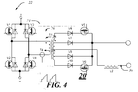
[0025] FIG.
4 shows a circuit diagram of a power supply 20 according to embodiments of
the disclosure. The power supply 20 includes various known components. The
components of
FIG. 2 and the figures to follow are listed in Table I for reference. As shown
in FIG. 4, a direct
current-alternate current (DC-AC) power converter 22 is arranged with a
plurality of switches,
shown as VI, V2, V3, V4.
9
CA 03005561 2018-05-16
WO 2017/103648
PCT/1B2015/059601
Al õ .=4 - Drivers of the main primary switches
All 13 - Summing nodes
Al 4 - Aniplifierlatt enuator
A15 - Leadhig edge modulation comparator
Al 6 - Amplifieriattenuator of the compensation ramp
Al 7 - Average current feedback amplifier
A18,19 - Lai edge modulation comparators
A20 - Feedback amplifier
A21 - Current sense amplifies
A22 - Primary current sense modifier
A23 - Sumnnrnz node
A24 - Integrator or other astatic regulator
A5,6 - Drivers oldie auxiliary (secondary or primary) switches
A5,6 - Drivers of the secondary primary :switches
A7,8 - Current amplitiersiattenuators
A9,10 - Current sense low pass filters
C.1 - Capacitor for DC voltage balance
1)12 - AND logic gates
D3,4 - RS triggers
D5 - OR logic gate
1)6 - Logic inverter
1)5 - PlarM Lagging edcfz7.e trigger1)9 - OR logic gate
DIO - Threshold reference pulse genelator
L2 - Secondary inductor
L$. 10 - Commutation inductances (or commutation leakage inductances)
NI PWM controller
S1,2 - Voltage controlled switches
S3 - Voltage controlled switch, normally open
S4 - Voltage controlled SINitch, norr1all3,, closed
Ti - Man converter transformer
T2 - Auxiliary converter transformer
1$ - Secondary current sensor
T4, T14 - Primary current sensors
T5,6 - Secondary auxiliary current sensors
.V02,03,01.2,013
V1..o4 - Primary switches of the main converter
V11...14 - Primary switches of the auxiliary converter
V20 - Rectifier function, rectify sipial of positive value
V71 + V27 - Concurrent rectifier
V23 + V24 - Concurent rectifier
V5,6 secondrsr), power switches
V7,8 - Main secondary rectifiers
- Auxiliary secondary rectifiers
CA 03005561 2018-05-16
WO 2017/103648
PCT/1B2015/059601
Table I. References used in the drawings
& - And logic function
- Or logic function
COMP - comparator
CS - Current sense input
Dtsh - Threshold reference value of PWM duty cycle
EA - Error amplifier
EAO, EAU - Error amplifier outputs
FBI - Current feedback
FBI] - Voltage feedback
it - Primary current signal
12 - Secondary current signal
lay - Average current reference
Ipeak - Peak current reference
121 - Second threslaold current value (low)
12H - First threshold current value (high)
KI .4 - Coefficients of amplificationlattenuation
OSC - Oscillator signal, double frequency of conversion
OFF - Disable integrator signal
PWMA - PWIVI signal phase A, lagging edge modulated
PW.M_B PIN7s1 signal phase a lagging edge modulated
MAIM C PW1kd sigial phase A, lagging & Ieadnig edge modulated
PVIM C PVINI sign d -rhose 4. lelm edo¨ inodthrei
PWM_D - signal he B, lagging & leading edge modulated
PINTM_D' PWIA signal phase B. leading edge modulated
RAMP - Ramp signal from the oscillator
RELOAD - Reload signal to integrator
V2A - Peak voltage of the auxiliary convertet
V?.B. - Peak voltage of the basic converter
V2L. - Low level of the peak voltage
- High Level of the peak voltage
z 11 - Primary windings
z21, z22, - Secondary windings
z3 I, z$2
Table I. (continued)
11
CA 03005561 2018-05-16
WO 2017/103648 PCT/1B2015/059601
[0026] In some embodiments these switches may be insulated gate bipolar
transistors (IGBT)
or MOSFET transistors as in known converters. In the embodiment shown in FIG.
4, the
switches may be arranged in a full bridge configuration. The DC-AC power
converter 22, acting
as a main DC-AC power converter, in this and other embodiments may be arranged
to receive a
first dc voltage, where the first DC voltage may be a rectified voltage based
upon an input
voltage from an AC power source (not shown). The DC-AC power converter 22 may
output an
ac voltage whose magnitude is determined by operation of the switches V1, V2,
V3, V4. As
detailed below the switches V1, V2, V3, V4, may be controlled by pulse width
modulation
(PWM) signals generated by a pulse width modulator (not separately shown).
[0027] As further shown in FIG. 4, the power supply 20 may further include
a transformer
stage 24. In various embodiments, the transformer stage 24 may include at
least one power
transformer to receive the ac voltage on a primary side of the transformer
stage and to output a
second ac voltage through a first set of secondary windings disposed on a
secondary side of the
transformer stage. In the particular embodiment illustrated in FIG. 4, just
one, main transformer
is shown, as Ti. As shown in this embodiment the transformer stage 24 includes
a first set of
secondary windings 28 and an auxiliary set of secondary windings 26. The
second set of
secondary windings 26 may be employed to extend the voltage range for welding
output as
detailed below. For example, under certain operation conditions, the first set
of secondary
windings may output a second ac voltage to rectifier V7, V8 to output dc
voltage used for
welding, based upon the input received from the DC-AC power converter 22.
Under other
12
CA 03005561 2018-05-16
WO 2017/103648 PCT/1B2015/059601
conditions, a third ac voltage from the auxiliary set of secondary windings 26
may be harnessed
to another rectifier to increase the welding dc voltage.
[0028] As further illustrated in FIG. 4, the power supply 20 may include a
pair of active
active unidirectional switches disposed on the secondary side to receive the
second ac voltage
from the auxiliary set of secondary windings 26. This pair of active switches
may rectify ac
voltage and output the dc voltage to a weld station 30. The first
unidirectional active switch is
shown as serial connection of rectifier V9 and active switch V5. The second
unidirectional
active switch is shown as serial connection of rectifier V10 and active switch
V6. In general, an
active unidirectional switch may be embodied as just one device.
[0029] FIG. 5 shows a circuit diagram of a power supply 40 according to
embodiments of
the disclosure. The power supply 40 includes various known components, as set
forth in Table
I., for example. In the arrangement of FIG.5, the power supply 40 may include,
in addition to the
DC--AC power converter 22, a transformer stage 42. In this embodiment the
transformer stage
42 includes a main converter transformer Ti and auxiliary converter
transformer T2. As shown
in this embodiment the transformer stage 42 includes a first set of secondary
windings 46
coupled to the main converter transformer Ti and an auxiliary set of secondary
windings 48
coupled to the auxiliary converter transformer T2. The second set of secondary
windings 48 may
be employed to extend the voltage range for welding output as detailed below
and generally
described above with respect to FIG. 2.
[0030] FIG. 6 shows a circuit diagram of a power supply 60 according to
embodiments of
the disclosure. In this embodiment the power supply 60 includes, a main DC ¨AC
power
converter 62, arranged as a two-switch forward converter or other power
converter operating
13
CA 03005561 2018-05-16
WO 2017/103648 PCT/1B2015/059601
with the limited maximum PWM duty cycle. In addition, the power supply 60
includes an
auxiliary DC¨AC power converter 64, which may be a low power converter also
arranged as a
two-switch forward converter or other power converter operating with the
limited maximum
PWM duty cycle. The auxiliary DC¨AC power converter 64 may operate in
different timing
phase with respect to the main DC¨AC power converter 62. As shown in FIG. 4,
the main DC¨
AC power converter 62 is coupled to a main converter transformer Ti and the
auxiliary DC¨AC
power converter 64 is coupled to the auxiliary converter transformer T2. The
main converter
transformer Ti may include main primary windings 67 and main secondary
windings 66, while
the auxiliary converter transformer T2 includes auxiliary secondary windings
69 and auxiliary
secondary windings 68. As shown, the main secondary winding is connected to
the main
rectifier V7 and the auxiliary secondary winding is connected to the auxiliary
rectifier V9.
Outputs of the rectifiers are connected in parallel. According to its
principle of operation, this
embodiment contains free-wheeling rectifier V8 on the output. As in the
embodiments of FIG. 4
and FIG. 5, additional voltage output through the auxiliary converter
transformer T2 may be
harnessed under low current conditions to increase the voltage output, as
generally shown in
FIG. 1.
[0031] FIG. 7 shows a circuit diagram of a power supply 80 according to
additional
embodiments of the disclosure. The power supply 80 may be arranged generally
as shown in
FIG. 2, with an additional exemplary control circuit, shown as control circuit
82. As generally
discussed above, control of the main converter, DC-AC power converter 22, may
be provided
using PWM control, in where the lagging edge of a pulse is used to control the
output from the
DC-AC power converter 22. Additionally, the secondary switches V5, V6 may be
controlled
using modulation of the leading edge of a pulse. This control is generally
shown in the control
14
CA 03005561 2018-05-16
WO 2017/103648 PCT/1B2015/059601
circuit 82 that outputs a PWM A signal, corresponding to a PWM signal having
phase A, where
the lagging edge is modulated. This signal may be sent to the switch VI and
switch V4, as
shown. The control circuit 82 also outputs a PWM B signal, corresponding to a
PWM signal
having phase B, where the lagging edge is also modulated. This signal may be
sent to the switch
V2 and switch V3, as shown. As suggested in FIG. 7, the phase of the PWM B
signal and
PWM A different from one another so the switches VI and V4 are in an OFF state
when the
switches V2 and V3 are in an ON state, and the switches V2 and V3 are in an
OFF state when
the switches VI and V4 are in an ON state.
[0032] As further illustrated in FIG. 7 the control circuit 82 may output a
PWM C signal,
corresponding to a PWM signal having phase A, where the lagging edge and
leading edge are
modulated. This signal may be sent to the secondary switch V5, as shown. The
control circuit
82 also may output a PWM D signal, corresponding to a PWM signal having phase
B, where the
leading edge and lagging edge are also modulated. This signal may be sent to
the secondary
switch V6 as shown. As suggested in FIG. 7, the phase of the PWM C signal and
PWM D
signal may differ from one another, in particular they complementary phases,
similarly as signal
PM/MA and PWM B.
[0033] Additionally, as further discussed below the control circuit 82 may
include a
component(s) acting as a variable time delay generator. The control circuit 82
may also include
control circuit includes logic and memory elements.
[0034] In order to adjust the level of voltage output to the weld station
30, the control circuit
82 may adjust operation of a set of primary switches, where the set of primary
switches may
include at least one primary switch, as exemplified by the primary switches
VI, V2, V3, V4; and
CA 03005561 2018-05-16
WO 2017/103648 PCT/1B2015/059601
the control circuit may adjust operation of a set of secondary switches where
the set of secondary
switches switches may include at least one secondary switch, as exemplified by
of the secondary
switches V5 and V6, in accordance with a sensed current. As shown in FIG. 5,
the power supply
80 may include a primary current sensor T4 arranged to measure a primary
current output by the
DC-AC power converter 22, and to generate a primary current sense signal. The
primary current
sense signal may be used to adjust the activation of primary switches V1, V2,
V3, V4 by the
principle of peak current mode control. The reference current Ipeak for the
peak current mode
control may be used to adjust the activation of secondary switch V5 and
secondary switch V6.
For example, since the leading edge of the PWM C signal and PWM D signal, sent
to
secondary switch V5 and V6, respectively, may be modulated by a controlled
time delay,
resulting in a variable time delay. The time delay may be adjusted according
to the output
current in the following manner. As the current increases, the reference peak
current also
increase, and consequently the variable time delay may increase so that the
variable time delay
becomes greater than one half of the switching period of the PWM A signal and
PWIVI B signal
at a first threshold value (see I2H of FIG 1). This results in the secondary
switch V5 and V6 not
being activated at all. In this manner, just the voltage output by the first
set of secondary
windings z21 and z22 is delivered to the weld station 30, through the
rectifiers V7, V8. The
maximum voltage can reach the level as represented by V2L (FIG. 1). Below the
first threshold
value the variable time delay may decrease along with decreased level of
output current value
down to second threshold value (see I2L of FIG. 1). In the current regime
between I2H and In, a
given reduction in current results in a given reduction of time delay where
the given reduction in
time delay increases activation of the secondary switch V5 and secondary
switch V6. This
increased activation results in a larger value of voltage drawn from the
auxiliary set of secondary
16
CA 03005561 2018-05-16
WO 2017/103648 PCT/1B2015/059601
windings 26, thus increasing the voltage output to the weld station 30. Below
a current
corresponding to the second threshold value I2L, the time delay for activating
the secondary
switch V5 and secondary switch V6 may become zero, so the secondary switch V5
and
secondary switch V6 may be activated without delay or permanently and
simultaneously
conducting. In this low current regime, the operation of secondary switches
(V5-V6) may be
not directly dependent of the current value and the maximum voltage output may
remain on the
high level over a range of current down to zero current.
[0035] Notably, the application of secondary switches in the power supply
80 may result in
instant or very fast change of the transformer ratio during the active phase
of the power
conversion. The current in the switches V1-V4 of the DC-AC power converter 22
is accordingly
changing rapidly. When a peak current mode control is applied, for PWM and for
the control of
the transformer core saturation, this rapid change of current may interrupt
the control principle,
reducing operation stability of the DC-AC power converter 22.
[0036] To address this issue, in the power supply 80 of FIG. 7, the primary
current sense
signal may be attenuated dynamically during the ON phase of the secondary
switches V5 and
V6. In the particular embodiment, the current sense is attenuated
proportionally to the ratio
between the main secondary winding and the main plus auxiliary secondary
windings. The
current sense signal may be disturbed, while after filtering may be still
available for control of
the operation of the power supply 80.
[0037] To address this issue, in other embodiments, the transformer stage
42 may be
substituted for two transformers such as in the power supply 40. In this
manner the presence of a
separate auxiliary transformer with two secondary windings allows a primary
current sensor to
17
CA 03005561 2018-05-16
WO 2017/103648 PCT/1B2015/059601
deliver current without rapid change. A drawback of this latter configuration
is that when the
auxiliary converter transformer T2 is not being used, a magnetization current
still circulates,
resulting in additional losses and there is no secure protection against the
saturation of the
transformer T2.
[0038] In various embodiments, the lagging edge of PWM signals controlling
secondary
switches may be modulated in the same way as for switches of a main converter,
by the same
control principle. Notably, just using modulation of the leading edge of PWM
signals in the
secondary switches may often be more effective. In this case the secondary
switch may be
switched off at some interval after the beginning of the opposite phase; thus
the switching off
process may be carried out with no current (zero current switching ZCS)
[0039] FIG. 8 shows a circuit diagram of a power supply 100 according to
further
embodiments of the disclosure. The power supply 100 may be arranged similarly
to power
supply 80, save for some differences including the differences discussed
below. In particular,
the power supply 100 includes a control circuit 102 having a set of RS flip-
flops, shown as RS
triggers D3, D4. The triggers are arranged to provide exclusively leading edge
modulation for
control of secondary switch V5 and secondary switch V6, to provide zero
current switching off.
As shown in FIG. 8, for example, the output from D3 is a PWM C' signal,
representing a
leading edge modulated PWM signal of phase A, where this signal is received by
the secondary
switch V5. Similarly, the output from D4 is a PWM D' signal, representing a
leading edge
modulated PWM signal of phase B, where this signal is received by the
secondary switch V6. In
order to secure zero current switching of the V5 and V6 secondary switches,
the lagging edges of
the PWM C' and PWM D signals may be further extended. The lagging edge may be
further
18
CA 03005561 2018-05-16
WO 2017/103648 PCT/1B2015/059601
delayed over the beginning of the PWM signals of a phase A and a phase B. In
different
embodiments, those delays may be fixed or may be current-dependent delay. In a
further variant
the zero current switching control may employ current sensing or voltage
sensing and additional
control logic.
[0040] FIG. 9 shows a circuit diagram of a power supply 120 according to
further
embodiments of the disclosure. The power supply 120 may be arranged similarly
to power
supply 80 or power supply 100, save for some differences including the
differences discussed
below. In addition to the control circuit 122, a distinguishing feature of the
power supply 120 is
the circuitry that provides for a primary current sense signal to be combined
with a secondary
current sense signal during the ON phase of the secondary switches, that is,
the secondary switch
V5 and secondary switch V6. As illustrated, a summing node All is arranged to
receive a
primary current sense signal from primary current sensor T4 and is also
arranged to receive a
secondary current sense signal from secondary current sensor T3. The summing
node All may
add these signals together during the ON phase of secondary switch V5 or
secondary switch V6.
The current sense signal may be disturbed, while after filtering may be used
for control of the
operation of the power supply 120.
[0041] FIG. 10 shows a circuit diagram of a power supply 140 according to
further
embodiments of the disclosure. The power supply 140 may be arranged similarly
to power
supply 80 or power supply 100, or power supply 120, save for some differences
including the
differences discussed below. In particular, the power supply 140 includes a
control circuit 142
and a pair of secondary auxiliary current sensors, shown as sensor T5 and
sensor T6. The sensor
19
CA 03005561 2018-05-16
WO 2017/103648 PCT/1B2015/059601
T5 is arranged to sense current between the auxiliary windings of the
secondary side of
transformer stage 24 and the secondary power switch V5. The sensor T6 is
arranged to sense
current between the auxiliary windings of the secondary side of transformer
stage 24 and the
secondary power switch V6. The sensor T6 and sensor T5, as well the primary
current sense
signal and the current sense signals from sensor T6 and sensor T5 may be
combined. This
provides a straightforward manner to control voltage output by the transformer
stage 24 in a
feedback loop by measuring g primary current as well as the auxiliary
secondary current.
[0042] FIG. 11 shows a circuit diagram of a power supply 160 according to
further
embodiments of the disclosure. The power supply 160 may be arranged similarly
to power
supply 80 or power supply 100, or power supply 120, or power supply 140, save
for some
differences including the differences discussed below. In particular, in the
control circuit 162,
signal switching may be applied after filtering. For example, the control
circuit 162 may include
a filter component, shown as a current sense low pass filter A9, and a current
sense low pass
filter A10 between the voltage controlled switch S1 and voltage controlled
switch S2,
respectively and primary current sensor T4.
[0043] FIG. 12 shows a circuit diagram of a power supply 180 according to
further
embodiments of the disclosure. The power supply 180 may be arranged similarly
to power
supply 80 or power supply 100, or power supply 120, or power supply 140, or
power supply 160
save for some differences including the differences discussed below. In
particular, in the control
circuit 182, two PWM comparators are provided, shown as the lagging edge
modulation
comparator Al8 and lagging edge modulation comparator A19.
CA 03005561 2018-05-16
WO 2017/103648 PCT/1B2015/059601
[0044] In all aforementioned embodiments, to create the variable time delay
of the leading
edge PWM modulation for the operation of the secondary switches, a threshold
current value, the
threshold current reference proportional to the current level I2L (FIG. 1), is
subtracted from the
peak current reference Ipeak in the summing node A13, and after amplification
or attenuation,
given to the comparator Al 5 to create adequate delayed signal by means of the
comparison with
certain ramp signal.
[0045] FIG. 13 shows an alternative embodiment of performing current sense
that may be
applied in conjunction with the circuitry and techniques of the aforementioned
embodiments.
The threshold current reference proportional to the current level I2L (FIG. 1)
is subtracted from
the secondary current sense value I2s proportional to the secondary current 12
in the summing
node A13, then after amplification or attenuation, given to the comparator Al
5 to create
adequate delayed signal by means of the comparison with certain ramp signal.
[0046] FIG. 14 shows a further embodiment of performing current sense that
may be applied
in conjunction with the circuitry and techniques of the aforementioned
embodiments. In this
embodiment, the threshold current proportional to the current level I2L (FIG.
1) is subtracted
from the primary current sense value Ics used as an input for peak current
mode control, in the
summing node A13, then after amplification or attenuation, given to the
comparator Al 5 to
create adequate delayed signal by means of the comparison with certain ramp
signal.
[0047] In various additional embodiments, signal switching may be applied
at any point
along the entire circuit of the lagging edge creation, either on analog or
discrete signals.
21
CA 03005561 2018-05-16
WO 2017/103648 PCT/1B2015/059601
[0048] FIG. 15 shows a circuit diagram of a power supply 200 according to
further
embodiments of the disclosure. The power supply 200 may be arranged similarly
to power
supply 60 with the addition of the control circuit 202
[0049] One novel aspect of the power supply 200 is the way of controlling
of a second two-
switch forward converter or any type converter operating with limited duty
cycle using the
modulation of the two pulse edges: lagging edge and leading edge. In
particular, in addition to a
primary current sensor T4 arranged to measure a primary current output by the
main power
converter 62, the power supply 200 includes a primary current sensor T14
coupled to measure
the current output of the auxiliary DC-DC power converter 64. In keeping with
the operation
principles discussed previously, the additional converter, the auxiliary power
DC¨AC converter
64, may not operate at all when the output current from the main power
converter 62 is larger
than the threshold value I2L. An advantage of the present embodiment is the
essentially lower
power of the auxiliary DC¨AC power converter 64. Another advantage is that the
auxiliary DC¨
AC power converter 64 may be enclosed as a separate module, giving a
manufacturer the
flexibility to produce power supplies with or without the extended voltage
characteristic feature.
[0050] FIG. 16 shows another embodiment where a power supply 200 includes
two two-
switch forward converters. According to its operating principle, this type of
the power converter
does not need primary current sense. In such an application the internally
generated ramp of the
control system 204 is used for leading and lagging edge pulse width
modulation.
[0051] FIG. 17 shows an extension of the control of the leading edge
modulation in
aforementioned systems, according to a further embodiment. The control system
205 comprises
two sources of the signal in the leading edge modulation, including a
proportional signal 206 and
22
CA 03005561 2018-05-16
WO 2017/103648 PCT/1B2015/059601
integral signal 207, which are connected to the input of the comparator Al 5
in a concurrent way.
This is schematically depicted by the implementation of two ideal rectifiers
V23 and V24. In
various embodiments, this function may be performed according to different
solutions effectively
performing the same function. In particular, the function may be performed
using a number
comparison in computer code. The proportional signal 206 is the same as in
previous
embodiments with the same principle of the operation. Schematically this
operation is depicted
by the summing node A13 and amplifier/attenuator A14. The integral signal 207
may be created
in the additional feedback loop. The actual duty cycle D is compared with a
certain threshold
value Dtsh in the summing node A23. The difference between those two values
may drive the
integrator or other astatic regulator A24, and the output of the integrator
A24 is the additional
source of the signal controlling the leading edge. The integrator A24 may be
periodically
reloaded with the last value of the delay taken after rectifiers V23 and V24
in purpose to increase
the speed of the operation. The operation principle is schematically depicted
by implementation
of the switch S3. The integrator can be temporarily switched off during the
transitions to
increase the speed of reaction of the control system. The operation principle
is schematically
depicted by implementation of the switch S4. For the same purpose a regulator
may be
cyclically present on different conditional instances.
[0052] FIG. 18 shows another control circuit 210 for control of the leading
edge modulation
in aforementioned systems according to an additional embodiment. There are two
sources of the
signal for the leading edge modulation, a proportional signal 206 and integral
signal 207,
connected to the input of the comparator Al 5 in a concurrent manner. The
proportional signal
206 is the same as in previous embodiments with the same principle of the
operation. The
integral signal 207 is created in the additional feedback loop. The summing
node A23 have
23
CA 03005561 2018-05-16
WO 2017/103648 PCT/1B2015/059601
negative input from the average current reference Jay, positive input from the
secondary current
12 and the positive input of the certain current offset AT. The output of the
summing node feeds
integrator or other astatic regulator A24, which delivers integral signal 207.
To increase the
speed of operation, the regulator A24 may be cyclically reloaded with the
actual value, as is
depicted by operation of the switch S4 and temporarily disabled, as is
depicted by operation of
the switch S3. For the same purpose regulator may be cyclically present on
different conditional
instances.
[0053] In some embodiments, a variable time delay may be increased by an
alternative
signal dependent on a value of a load connected to the welding apparatus. In
further
embodiments, the alternative signal comprises a signal received from a
regulator comprising an
integrator or other regulator, the regulator being fed by a difference between
values of actual
duty cycles of the first and second PWM signal and a reference duty cycle
value. In additional
embodiments, the alternative signal comprises a signal received from a
regulator comprising an
integrator or other regulator, the regulator being fed by a difference between
an actual secondary
current and a reference secondary current. In other embodiments the
alternative signal may be
temporarily switched off or preset to improve a dynamic response of the
apparatus. In further
embodiments, the alternative signal may be temporarily switched off or preset
to improve a
dynamic response of the apparatus. In still other embodiments, the alternative
signal may be
cyclically updated with an actual value of the delay to improve a dynamic
response of the
apparatus.
[0054] The present disclosure is not to be limited in scope by the specific
embodiments
described herein. Indeed, other various embodiments of and modifications to
the present
24
CA 03005561 2018-05-16
WO 2017/103648 PCT/1B2015/059601
disclosure, in addition to those described herein, will be apparent to those
of ordinary skill in the
art from the foregoing description and accompanying drawings.
[0055] Thus, such other embodiments and modifications are intended to fall
within the scope
of the present disclosure. Furthermore, although the present disclosure has
been described herein
in the context of a particular implementation in a particular environment for
a particular purpose,
those of ordinary skill in the art will recognize that its usefulness is not
limited thereto and that
the present disclosure may be beneficially implemented in any number of
environments for any
number of purposes. In particular, all embodiments of the controls, described
schematically by
means of basic functions, may be implemented in a form of computer code or in
digital hardware
form. Thus, the claims set forth below are to be construed in view of the full
breadth and spirit
of the present disclosure as described herein.