Note: Descriptions are shown in the official language in which they were submitted.
CA 03008595 2018-06-14
DEECRIPTION
Title of Invention
ELECTROCHROMIC APPARATUS
Technical Field
The present invention relates to an electrochromic device.
Background Art
Electrochromism is a phenomenon where a redox reaction
is performed to reversibly change a color by applying voltage.
An electrochromic element utilizing the electrochromism has
been intensively studied to realize applications derived from
characteristics of the electrochromism.
Since the electrochromic element can vary light
transmittance thereof according to electric signals, the
electrochromic element has an advantage that a user can freely
control the light transmittance. Therefore, developments have
been made to realize electrochromic devices for practical use,
such as light-adjusting spectacles using the electrochromic
elements as lenses.
For example, proposed is an electrochromic device where
an electrochromic element and a power source are electrically
connected via a rim by pressure-bonding the conductive rim
holding a periphery of the electrochromic element to an electrode
1
CA 03008595 2018-06-14
pad exposed at an edge surfa`ce of the electrochromic element (see,
for example, PTL 1). Moreover, proposed is an electrochromic
device where an electrochromic element and a power source are
electrically connected with anisotropic conductive rubber nipped
between an electrode pad and a rim (see, for example, PTL 2).
Citation List
Patent Literature
PTL 1: Japanese Unexamined Utility Model Application
Publication No. 02-138720
PTL 2: Japanese Patent No. 5511997
Summary of Invention
Technical Problem
The present invention has an object to provide an
electrochromic device having excellent durability of electrical
connection.
Solution to Problem
As means for solving the above-described problems, an
electrochromic device of the present invention includes an
electrochromic element including a protrusion on a periphery of
the electrochromic element, and a frame holding the
electrochromic element. The protrusion includes an electrode
2
CA 03008595 2018-06-14
P,..
pad and the frame includes a connecting member configured to
electrically connect to the electrode pad.
Effects of Invention
The present invention can provide an electrochromic
device having excellent durability of electrical connection.
Mode for Carrying out the Invention
FIG. 1 is a schematic view illustrating one example of an
electrochromic device of the present invention.
FIG. 2A is a schematic view illustrating a first laminate
constituting part of layers of an electrochromic element used in
the electrochromic device of FIG. 1.
FIG. 2B is a schematic view illustrating a second laminate
constituting another part of layers of the electrochromic element
used in the electrochromic device of FIG. 1.
FIG. 2C is a schematic view illustrating a state where the
first laminate illustrated in FIG. 2A and the second laminate
illustrated in FIG. 2B are assembled together.
FIG. 2D is a schematic view illustrating a state where the
electrochromic element of FIG. 2C was shaped through
thermoforming.
FIG. 2E is a schematic view illustrating a state where a
resin layer is formed on the electrochromic element of FIG. 2D.
3
CA 03008595 2018-06-14
FIG. 3 is a schematic view illustrating another example of
a layer structure of the electrochromic element used in the
electrochromic device of FIG. 1.
FIG. 4 is a schematic view illustrating one example of a
front surface and cross-section of the electrochromic element
used in the electrochromic device of FIG. 1.
FIG. 5A is a schematic view illustrating another example
of a front surface and cross-section of the electrochromic element
used in the electrochromic device of FIG. 1.
FIG. 5B is a schematic view illustrating another example
of a front surface and cross-section of the electrochromic element
used in the electrochromic device of FIG. 1.
FIG. 6 is an explanatory view illustrating connection
between electrode pads disposed in the electrochromic elements
of FIG. 4 and connecting members disposed on a frame.
FIG. 7A is a schematic view illustrating a cross-section of a
state where an electrode pad is disposed in the electrochromic
element of FIG. 4.
FIG. 7B is a schematic view illustrating a cross-section of
a state where a connecting member is connected to the electrode
pad of the electrochromic element of FIG. 7A.
FIG. 8 is a schematic view illustrating a cross-section of
the electrochromic element of Comparative Example 1.
4
CA 03008595 2018-06-14
=
Description of Embodiments'
(Electrochromic device)
An electrochromic device of the present invention includes
an electrochromic element including a protrusion on a periphery
thereof and a frame holding the electrochromic element. The
protrusion includes an electrode pad and the frame includes a
connecting member configured to electrically connect to the
electrode pad. The electrochromic device may further include
other members according to the necessity.
The electrochromic device of the present invention is based
on insights that it is difficult for an electrochromic device known
in the art to obtain durability of electrical connection because a
screw for securing the rim in contact with the electrode pad on an
edge face of the electrochromic element is loosened or an area of
the electrode pad is small.
The electrochromic element includes a pair of electrode
layers (a first electrode layer and second electrode layer
described later) to which electric signals are applied. The
electrode pad that is to be electrically connected to the electrode
layer is disposed on the protrusion. The electrode pad is
included for the purpose of improving durability of electrical
connection between an edge of the electrode layer exposed from
an edge face of the protrusion and the connecting member on the
side of the frame connected to a power source. An area that can
5
CA 03008595 2018-06-14
be in contact with the connOting member can be extended by the
electrode pad. Moreover, giving the protrusion a structure
where the protrusion can locked with the connecting member can
fix the entire electrochromic element and can obtain electrical
connection having excellent durability.
Examples of use of the electrochromic device include
electrochromic light-adjusting spectacles that use the
electrochromic element as lenses and can adjust light
transmittance depending on electric signals applied to the
electrochromic element.
<Electrochromic element>
The electrochromic element is not particularly limited and
may be appropriately selected depending on the intended purpose,
as long as the electrochromic element has the protrusion on a
periphery thereof.
A shape of the electrochromic element is not particularly
limited and may be appropriately selected depending on the
intended purpose. In the case where the electrochromic device
of the present invention is used as a pair of electrochromic
light-adjusting spectacles, the electrochromic element is
preferably in the shape of a lens where an outer shape of the
electrochromic element corresponds to a shape of a rim of the
frame.
Note that, a layer structure of the electrochromic element
6
CA 03008595 2018-06-14
1
t
e
=
will be described later.
<<Protrusion>>
The protrusion is not particularly limited and may be
appropriately selected depending on the intended purpose, as
long as the protrusion includes the electrode pad.
The number of the protrusion(s) is not particularly limited
and may be appropriately selected depending on the intended
purpose. A plurality of the protrusions may be disposed. For
the purpose of applying voltage between a pair of the electrodes
included in the electrochromic element, the number of the
protrusions may be 2.
When the number of the protrusions is 2 or more, example
of an arrangement of the protrusions on the periphery of the
electrochromic element include an arrangement where the
protrusions are disposed to next to one another to shorten wiring
of the line, and an arrangement where a plurality of the
protrusions are disposed on both the sides of the electrochromic
element in order to fix the electrochromic element with a
mechanically desirable balance.
Examples of a shape of the protrusion include rectangular
shapes and semicircle shapes.
A formation method of the protrusion is not particularly
limited and may be appropriately selected depending on the
intended purpose. When the electrochromic element is used as a
7
CA 03008595 2018-06-14
1 )
lens, examples of the formation method of the protrusion include
a method where the protrusion is formed during lens shape
processing to cut to match an outer shape of the electrochromic
element with a shape of a rim of the frame.
-Electrode pad-
The electrode pads are electrically connected to a pair of
the electrode layers included in the electrochromic element and
are brought into contact with the connecting members disposed
on the rim of the frame to electrically connect to the connecting
members. Specifically, the electrode pads act as contact points
for electrically connecting a power source, which is electrically
connected to the connecting members, to the electrochromic
elements.
As a structure of the electrode pad, the electrode pad is
disposed in a manner that the electrode pad is wound around the
protrusion and is preferably fixed onto the protrusion with the
conductive adhesive.
A method for electrically connecting the electrode layer to
the electrode pad is not particularly limited and may be
appropriately selected depending on the intended purpose. The
method is preferably a method where edges of a pair of the
electrode layers are electrically connected to the separate
electrode pads through application of a conductive adhesive.
In order to prevent short circuit between the pair of the
8
CA 03008595 2018-06-14
1
electrode layers via the conductive adhesive, moreover, the edge
face of either of the electrode layers is preferably exposed from
the edge of the electrochromic element that is in the form of the
laminate in the region where the conductive adhesive is applied.
Examples of the electrode pad include metal foil.
Examples of the metal foil include copper foil and aluminium foil.
The conductive adhesive is not particularly limited and
may be appropriately selected depending on the intended purpose.
Examples of the conductive adhesive include silver paste.
<<Layer structure of electrochromic element>>
A layer structure of the electrochromic element is not
particularly limited and may be appropriately selected depending
on the intended purpose. The layer structure is preferably a
first embodiment or second embodiment described below.
-First embodiment-
A layer structure of the electrochromic element according
to a first embodiment includes a first substrate, a first electrode
layer, an electrochromic layer, an insulating inorganic-particle
layer, a second electrode layer, and a second substrate in the
order as mentioned, and includes an electrolyte between the first
electrode layer and the second electrode layer.
--First substrate and second substrate--
The first substrate and the second substrate (may be
simply referred to as a "substrate" hereinafter, when it is not
9
CA 03008595 2018-06-14
necessary to identify the first substrate or the second substrate)
are not particularly limited and any of resin materials that can
be used for thermoforming and known in the art is appropriately
selected as it is, depending on the intended purpose. Examples
of the substrate include resin substrates, such as polycarbonate
resins, acrylic resins, polyethylene resins, polyvinyl chloride
resins, polyester resins, epoxy resins, melamine resins, phenol
resins, polyurethane resins, and polyimide resins.
In order to enhance water vapor-barrier properties, gas
barrier properties, and visibility, moreover, a surface of the
substrate may be coated with a transparent insulating
inorganic-particle layer, an antireflection layer, etc.
A shape of the substrate is not particularly limited and
may be appropriately selected depending on the intended purpose.
Examples of the shape include oval shapes and rectangular
shapes. When the electrochromic device is used as the
electrochromic light-adjusting spectacles, moreover, the first
substrate is used as a lens, and an outer shape of the first
substrate may be shaped to match a rim of the frame.
--First electrode layer and second electrode layer--
A material of each of the first electrode layer and the
second electrode layer (may be simply referred to as an "electrode
layer" hereinafter, when it is not necessary to identify the first
electrode layer or the second electrode layer) is not particularly
CA 03008595 2018-06-14
I }
limited and may be appropritttely selected depending on the
intended purpose, as long as the material is a material that is
transparent and has conductivity. Examples of the material
include tin-doped indium oxide (may be referred to as "ITO"
hereinafter), fluorine-doped tin oxide (may be referred to as
"FTO" hereinafter), and antimony-doped tin oxide (may be
referred to as "ATO" hereinafter). Among the above-listed
examples, the material is preferably a material including at least
one selected from indium oxide (may be referred to as "In oxide"
hereinafter), tin oxide (may be referred to as "Sn oxide"
hereinafter), and zinc oxide (may be referred to as "Zn oxide"
hereinafter) formed by vacuum film formation because the
above-mentioned materials are materials that can be easily
formed into a film by sputtering, as well as excellent
transparency and electrical conductivity can be obtained.
Among the above-listed examples, InSnO, GaZnO, SnO, In203,
and ZnO are particularly preferable. Moreover, a transparent
network electrode of silver, gold, carbon nanotubes, or metal
oxide, or a composite layer of the above-listed electrodes is also
effective.
An average thickness of the electrode layer is not
particularly limited and may be appropriately selected depending
on the intended purpose. The average thickness of the electrode
layer is preferably adjusted to obtain a necessary electric
11
CA 03008595 2018-06-14
resistance value for an electtochromic redox reaction. When
ITO is used, the average thickness is preferably 50 nm or greater
but 500 nm or less.
A formation method of the electrochromic layer is not
particularly limited and may be appropriately selected depending
on the intended purpose. Examples of the formation method
include vacuum film formation methods and coating film
formation methods.
Examples of the vacuum film formation methods include
vacuum vapor deposition, sputtering, and ion plating.
Examples of the coating film formation methods include
spin coating, casting, microgravure coating, gravure coating, bar
coating, roll coating, wire bar coating, dip coating, slit coating,
capillary coating, spray coating, nozzle coating, and various
printing methods, such as gravure printing, screen printing, flexo
printing, offset printing, reverse printing, and inkjet printing.
--Electrochromic layer--
The electrochromic layer is not particularly limited and
may be appropriately selected depending on the intended purpose,
as long as the electrochromic layer includes an electrochromic
compound.
As a material of the electrochromic compound, any of
electrochromic compound materials known in the art, such as
dye-based electrochromic compound materials, polymer-based
12
CA 03008595 2018-06-14
1
electrochromic compound mdterials, metal complex-based
electrochromic compound materials, and metal oxide-based
electrochromic compound materials can be used.
Examples of the dye-based electrochromic compound and
the polymer-based electrochromic compound include:
low-molecular organic electrochromic compounds, such as
azobenzene-based compounds, anthraquinone-based compounds,
diarylethene-based compounds, dihydroprene-based compounds,
dipyridine-based compounds, styryl-based compounds,
styrylspiropyran-based compounds, spirooxazine-based
compounds, spirothiopyran-based compounds, thioindigo-based
compounds, tetrathiafulvalene-based compounds, terephthalic
acid-based compounds, triphenylmethane-based compounds,
triphenylamine-based compounds, naphthopyran-based
compounds, viologen-based compounds, pyrazoline-based
compounds, phenazine-based compounds,
phenylenediamine-based compounds, phenoxazine-based
compounds, phenothiazine-based compounds,
phthalocyanine-based compounds, fluoran-based compounds,
flugide-based compounds, benzopyran-based compounds, and
metallocene-based compounds; and conductive polymer
compounds, such as polypyrrole, polyaniline, and polythiophene.
The above-listed examples may be used alone or in combination.
Among the above-listed examples, viologen-based compounds (see,
13
CA 03008595 2018-06-14
1
i
for example, Japanese Patent No. ,3955641 and Japanese
Unexamined Patent Application Publication No. 2007-171781)
and dipyridine-based compounds (see, for example, Japanese
Unexamined Patent Application Publication No. 2007-171781 and
Japanese Unexamined Patent Application Publication No.
2008-116718) are preferable. Among the above-listed preferable
examples, the viologen-based compounds or the dipyridine-based
compounds are preferable because the electrochromic compound
can exhibit an excellent color value at the time of coloring and
decoloring even when voltage applied between a display electrode
and a counter electrode is low, and the dipyridine-based
compounds represented by General Formula 1 below are more
preferable because a color value of excellent coloring is exhibited.
[General Formula 1]
// ________________________ \ r/õ.= ------ -..,=N //õ.. ------ ...,
/..,..- ------ ...,\N ¨\ / R2
N+ ____ iO _____ iit1/4113; N+ 2X¨
R/ \ ___________________________ .1 \ y
n m I
1 5
In General Formula 1 above, R1 and R2 are each
independently an alkyl group having from 1 through 8 carbon
atoms or an aryl group both of which may have a sub stituent,
where at least one of R1 and R2 includes a substituent selected
from COOH, PO(OH)2, and Si(OCkH2k+1)3 (with the proviso that k
is from 1 through 20). X- is a monovalent anion. X- is not
particularly limited as long as X- can stably form a pair with a
14
CA 03008595 2018-06-14
A
cation, and examples of X- iriclude, a Br ion (Br-), a Cl ion (CI), a
C104 ion (C104-), a PF6 ion (PF6-), and BF4 ion (BF4-). n, m, and
1 are 0, 1, or 2. A, B, and C are each independently an alkylene
group having from 1 through 20 carbon atoms, an arylene group,
or a divalent heterocycle group, all of which may have a
substituent.
Examples of the metal complex-based electrochromic
compound and the metal oxide-based electrochromic compound
include inorganic electrochromic compounds, such as titanium
oxide, vanadium oxide, tungsten oxide, indium oxide, iridium
oxide, nickel oxide, and Prussian blue. The above-listed
examples may be used alone or in combination.
Moreover, the electrochromic compound is preferably the
organic electrochromic compound, and is more preferably the
organic electrochromic compound born on conductive particles or
semiconductive particles. The electrochromic layer including
the organic electrochromic compound born on the conductive
particles or the semiocnductive particles is advantageous because
electrons are efficiently injected to the organic electrochromic
compound utilizing a large surface area of the conductive
particles or the semiconductive particles and a resultant
electrochromic device achieves high speed response compared to
electrochromic devices known in the art. Moreover, another
advantage is that a transparent film can be formed as a display
CA 03008595 2018-06-14
layer using the conductive particles or the semiconductive
particles, and a high coloring density of an electrochromic dye
can be obtained. Furthermore, another advantage is that a
plurality of types of organic electrochromic compounds can be
born on the conductive particles or the semiconductive particles.
The conductive particles or the semiconductive particles
are not particularly limited and may be appropriately selected
depending on the intended purpose. Examples of the conductive
particles or the semiconductive particles include particles of
metal oxide.
Examples of a material of the metal oxide include titanium
oxide, zinc oxide, tin oxide, zirconium oxide, cerium oxide,
yttrium oxide, boron oxide, magnesium oxide, strontium titanate,
potassium titanate, barium titanate, calcium titanate, calcium
oxide, ferrite, hafnium oxide, tungsten oxide, iron oxide, copper
oxide, nickel oxide, cobalt oxide, barium oxide, strontium oxide,
vanadium oxide, and metal oxides including as a main component,
aminosilicic acid, calcium phosphate, aminosilicate, etc. The
above-listed examples may be used alone or in combination.
Among the above-listed examples, in view of electrical
properties, such as electric conductivity, and physical properties,
such as optical characteristics, one selected from the group
consisting of titanium oxide, zinc oxide, tin oxide, zirconium
oxide, iron oxide, magnesium oxide, indium oxide, and tungsten
16
CA 03008595 2018-06-14
3
3
oxide, or a mixture thereof i. preferable because a color display
having excellent coloring and decoloring response speed is
realized, and titanium oxide is more preferable because a color
display having more excellent coloring and decoloring response
speed is realized.
Shapes of the conductive particles or the semiconductive
particles are not particularly limited. The shapes are preferably
shapes having large surface areas per unit volume (referred to as
a specific surface area hereinafter) in order to efficiently bear the
electrochromic compound.
When the particles are aggregates of nanoparticles, for
example, the particles have a large specific surface area, an
electrochromic compound is more efficiently born thereon, and as
a result, a display contrast ratio of coloring and decoloring is
excellent.
An average thickness of the electrochromic layer is not
particularly limited and may be appropriately selected depending
on the intended purpose. The average thickness is preferably
0.2 p.m or greater but 5.0 pm or less. Use of the electrochromic
layer having the average thickness within the above-mentioned
preferable range is advantageous because a production cost can
be reduced, coloring can be suppressed, and visibility is unlikely
to be reduced, as well as easily achieving a desired coloring
density.
17
CA 03008595 2018-06-14
t
t
The organic electrochromic =layer born on the conductive
particles or the semiconductive particles can be formed by
vacuum film formation, but is preferably formed by applying a
particle dispersion paste in view of productivity.
A formation method of the electrochromic layer is not
particularly limited and may be appropriately selected depending
on the intended purpose. Examples of the formation method
include vacuum film formation methods and coating film
formation methods.
Examples of the vacuum film formation methods include
vacuum vapor deposition, sputtering, and ion plating.
Examples of the coating film formation methods include
spin coating, casting, microgravure coating, gravure coating, bar
coating, roll coating, wire bar coating, dip coating, slit coating,
capillary coating, spray coating, nozzle coating, and various
printing methods, such as gravure printing, screen printing, flexo
printing, offset printing, reverse printing, and inkjet printing.
As a formation method of the organic electrochromic layer
born on the conductive particles or the semiconductive particles,
for example, the conductive particles or semiconductive particles
having particle diameters of 5 nm or greater but 50 nm or less
may be sintered on a surface of the electrode layer and the
organic electrochromic compound having a polar group, such as
phosphonic acid, a carboxyl group, and a silanol group, may be
18
CA 03008595 2018-06-14
,
4
allowed to bear on surfaces o'f the sintered particles.
--Insulating inorganic-particle layer--
The insulating inorganic-particle layer is a layer
configured to separate the first electrode layer and the second
electrode layer in order to electrically insulate between the first
electrode layer and the second electrode layer.
A material of the insulating inorganic-particle layer is not
particularly limited and may be appropriately selected depending
on the intended purpose. The material is preferably an organic
material, an inorganic material, or a composite thereof having
high insulation, high durability, and excellent film formation
properties.
Examples of a formation method of the insulating
inorganic-particle layer include formation methods known in the
art, such as sintering, extraction, foaming where a
macromolecular polymer etc. is heated or degassed to foam, phase
transferring where phase separation of a mixture of
macromolecules is performed by controlling a good solvent and a
poor solvent, and radial-ray irradiation where various radial rays
are applied to form fine pores.
Examples of the sintering include a method where
macromolecular particles or inorganic particles are added to a
binder etc. to partially fuse the particles and pores formed
between the particles are used.
19
CA 03008595 2018-06-14
Examples of the extrabtion include a method where a layer
composed of an organic material or inorganic material soluble to
a solvent and a binder insoluble to a solvent, etc., is formed,
followed by dissolving the organic material or inorganic material
with the solvent to form pores.
The insulating inorganic-particle layer is not particularly
limited and may be appropriately selected depending on the
intended purpose. Examples of the insulating inorganic-particle
layer include a resin-mixed particle film formed of metal oxide
particles (e.g., Si02 particles and A1203 particles) and a resin
binder, a porous organic film (e.g., a polyurethane resin and a
polyethylene resin), and an inorganic insulation material film
formed on a porous film.
A number average particle diameter of primary particles of
the metal oxide particles constituting the insulating
inorganic-particle layer is preferably 5 nm or greater but 300 nm
or less, and more preferably 10 nm or greater but 80 nm or less.
The particles are preferably porous for permeation of an
electrolyte solution, and in association with the particle
diameters, metal oxide particles having large particle diameters
are more preferable in order to increase a void ratio.
The insulating inorganic-particle layer is preferably used
in combination with an inorganic film. As a material of the
inorganic film, a material including ZnS is preferable. A film of
CA 03008595 2018-06-14
,
ZnS can be formed at high speed hy sputtering without damaging
an electrochromic layer.
Examples of the material including ZnS as a main
component include ZnS¨Si02, ZnS¨SiC, ZnS¨Si, and ZnS¨Ge. In
order to excellently maintain crystallinity when the insulating
inorganic-particle layer is formed, the ZnS content is preferably
50 mol% or greater but 90 mol% or less. Accordingly, ZnS¨Si02
(molar ratio = 8/2), ZnS¨Si02 (molar ratio = 7/3), ZnS, and
ZnS¨ZnO-1n203¨Ga203 (molar ratio = 60/23/10/7) are more
preferable.
Use of the above-mentioned material of the insulating
inorganic-particle layer can achieve an excellent insulation effect
with a thin film and can prevent low film strength and peeling of
the film due to the formation of multilayers.
--Electrolyte--
The electrolyte is a solid electrolyte. The electrolyte is
disposed between the first electrode layer and the second
electrode layer and is held in a cured resin.
The electrolyte is not particularly limited and may be
appropriately selected depending on the intended purpose, but
inorganic particles configured to control an average thickness of
the electrolyte are preferably mixed in the electrolyte.
After forming the insulating inorganic-particle layer in
advance, moreover, the electrolyte is preferably applied, as a
21
CA 03008595 2018-06-14
. i
solution in which the electrolyte is mixed with the curable resin,
onto the insulating inorganic-particle layer in a manner that the
solution permeates the insulating inorganic-particle layer,
followed by curing using light or heat. The electrolyte may be
formed into a film by applying a solution in which the inorganic
particles and the curable resin are mixed onto the electrochromic
layer and curing the solution with light or heat.
In the case where the electrochromic layer is a layer
including an electrochromic compound born on conductive or
semiconductive nanoparticles, moreover, a solution in which the
curable resin and the electrolyte are mixed is applied to permeate
the electrochromic layer, followed by curing the solution with
light or heat to form a film of the electrochromic layer.
Examples of the electrolyte solution include liquid
electrolytes, such as ionic liquids, and solutions each obtained by
dissolving a solid electrolyte in a solvent.
As the electrolyte, for example, inorganic ion salts (e.g.,
alkali metal salts and alkaline earth metal salts), quaternary
ammonium salts, and supporting electrolytes of acids or alkalis
can be used. Specific examples thereof include
1-ethyl-3-methylimidazolium salt, LiC104, LiBF4, LiAsF6, LiPF6,
LiCF3S03, LiCF3C00, KC1, NaC103, NaCl, NaBF4, NaSCN, KBF4,
Mg(C104)2, and Mg(BF4)2. The above-listed examples may be
used alone or in combination.
22
CA 03008595 2018-06-14
Examples of the solveht inciude propylene carbonate,
acetonitrile, y-butyrolactone, ethylene carbonate, sulfolane,
dioxolane, tetrahydrofuran, 2-methyltetrahydrofuran,
dimethylsulfoxide, 1,2-dimethoxyethane,
1,2-ethoxymethoxyethane, polyethylene glycol, and alcohols.
The above-listed examples may be used alone or in combination.
Examples of the curable resin include: photocurable resins,
such as acrylic resins, urethane resins, epoxy resins, vinyl
chloride resins, ethylene resins, melamine resins, and phenol
resins; and heat-curable resins. Among the above-listed
examples, a material having high compatibility to the electrolyte
is preferable, and derivatives of ethylene glycol, such as
polyethylene glycol and polypropylene glycol, are more preferable.
As the curable resin, moreover, a photocurable resin is preferable
because an element can be produced at a low temperature within
a short time period compared to a method where a thin film is
formed by thermal polymerization or evaporation of a solvent.
Among the electrolytes where the above-mentioned
materials are combined, a solid liquid between a matrix polymer
including an oxyethylene chain or an oxypropylene chain and
ionic liquid is particularly preferable because both hardness and
high ionic conductivity are easily achieved.
The inorganic particles are not particularly limited as long
as the inorganic particles can form a porous layer to retain an
23
CA 03008595 2018-06-14
,
electrolyte and a curable resin. In view of stability of an
electrochromic reaction and visibility, a material of the inorganic
particles is preferably a material having high insulation
properties, transparency, and durability. Specific examples of
the material include oxides or sulfides of silicon, aluminium,
titanium, zinc, tin, etc., or mixtures thereof.
A number average particle diameter of primary particles of
the inorganic particles is not particularly limited and may be
appropriately selected depending on the intended purpose. The
number average particle diameter is preferably 10 nm or greater
but 10 p.m or less, and more preferably 10 nm or greater but 100
nm or less.
-Second embodiment-
A layer structure of the electrochromic element according
to a second embodiment includes the first substrate, the first
electrode layer, the electrochromic layer, an insulating porous
layer, and the second electrode layer having through holes, and a
deterioration prevention layer in the order as mentioned, and
includes an electrolyte between the first electrode layer and the
deterioration prevention layer.
In the second embodiment, layers different from those in
the first embodiment will be described below.
--Insulating porous layer--
The insulating porous layer has a function of retaining the
24
CA 03008595 2018-06-14
electrolyte included in the luaded electrolyte solution, as well as
separating the first electrode layer and the second electrode layer
to electrically insulate between the first electrode layer and the
second electrode layer having the through holes.
The insulating porous layer is not particularly limited and
may be appropriately selected depending on the intended purpose.
The insulating porous layer preferably includes insulating metal
oxide particles.
Examples of the metal oxide particles include Si02
particles and A1203 particles. Among the above-listed examples,
Si02 particles are preferable. Use of Si02 particles as the
insulating metal oxide particles is advantageous because nano
particles whose number average particle diameter of primary
particles is 5 nm or greater but 500 nm or less and a dispersion
coating liquid of the nanoparticles are obtained at low cost.
Examples of the insulating porous layer include a
polymer-mixed particle film including the metal oxide particles
and a polymer binder, a porous organic film, and an inorganic
insulating material film formed into a porous film.
Examples of the porous organic film include a
polyurethane resin and a polyethylene resin.
A material of the insulating porous layer is not
particularly limited and may be appropriately selected depending
on the intended purpose. An organic material, inorganic
CA 03008595 2018-06-14
material, or composite thereof having high insulation properties
and durability and excellent film formability is preferably used.
An average thickness of the insulating porous layer is not
particularly limited and may be appropriately selected depending
on the intended purpose. The average thickness is preferably 50
nm or greater but 10 pm or less.
Average roughness (Ra) of the insulating porous layer
depends on an average thickness of the second electrode layer
having the through holes. For example, the average roughness
(Ra) is preferably less than 100 nm, when an average thickness of
the second electrode layer having the through holes is 100 nm.
Use of the insulating porous layer having the average roughness
of less than 100 nm is advantageous because surface resistance of
the second electrode layer having the through holes is not
significantly impaired, which is unlikely to cause display
failures.
The insulating inorganic-particle layer is preferably used
in combination with an inorganic film. As a material of the
inorganic film, a material including ZnS as a main component is
preferable. A film of ZnS can be formed at high speed by
sputtering without damaging an electrochromic layer.
Examples of the material including ZnS as a main
component include ZnS¨Si02, ZnS¨SiC, ZnS¨Si, and ZnS¨Ge. In
order to excellently maintain crystallinity when the insulating
26
CA 03008595 2018-06-14
r
r
inorganic-particle layer is formed, the ZnS content is preferably
50 mol% or greater but 90 mol% or less. Accordingly, ZnS¨Si02
(molar ratio = 8/2), ZnS¨Si02 (molar ratio = 7/3), ZnS, and
ZnS¨ZnO-1n203¨Ga203 (molar ratio = 60/23/10/7) are more
preferable.
Use of the above-mentioned material of the insulating
inorganic-particle layer can achieve an excellent insulation effect
with a thin film and can prevent low film strength and peeling of
the film due to the formation of multilayers.
--Second electrode layer having through holes--
The second electrode layer having the through holes is not
particularly limited and may be appropriately selected depending
on the intended purpose, as long as the second electrode layer is
disposed to face the first electrode layer and has through holes
therein.
Compared to the electrode layer, the second electrode layer
having the through holes is identical other than the through
holes formed along a thickness direction of the electrode. As a
material of the second electrode layer having the through holes,
the same materials to the materials of the first electrode layer
and the second electrode layer can be used.
The through holes are not particularly limited and may be
appropriately selected depending on the intended purpose. The
through holes are preferably a large number of fine through
27
CA 03008595 2018-06-14
holes.
Diameters of the through holes are not particularly limited
and may be appropriately selected depending on the intended
purpose. The diameters are preferably 10 nm (0.01 pm) or
greater but 100 pm or less. When the diameters of the through
holes are within the preferable range, advantageously,
occurrences of a problem that permeation of electrolyte ions
becomes poor can be reduced and occurrences of a problem where
the size of the through holes becomes a level that can be visually
observed from the above of the through holes (the size of one pixel
electrode level in a typical display) can be reduced.
A pore area rate (hole density) of the through holes
disposed in the second electrode layer having the through holes
relative to a surface area of the second electrode layer having the
through holes is not particularly limited and may be
appropriately selected depending on the intended purpose. The
hole density is preferably 0.01% or greater but 40% or less. The
hole density within the preferable range is advantageous,
because permeation of the electrolyte is excellent, a problem is
unlikely to occur during the driving of coloring and decoloring, a
surface resistance of the second electrode does not become
excessively large, and chromic defects that may be caused by a
large area of a region where the second electrode layer having the
through holes is not present is unlikely to occur.
28
CA 03008595 2018-06-14
--Deterioration prevention la'yer--
Use of the deterioration prevention layer can expect an
effect of stabilizing an electrochemical reaction because of a
reverse reaction of the electrochromic layer performed, and an
effect of reducing a potential difference required for an
electrochromic reaction.
The deterioration prevention layer is not particularly
limited and may be appropriately selected depending on the
intended purpose. In the case where the electrochromic layer
colors through reduction, it is preferable that an oxidization
reaction occur in the deterioration prevention layer.
A material of the deterioration prevention layer is not
particularly limited and may be appropriately selected depending
on the intended purpose. Since the material can be regarded as
an (almost color-unchanging) electrochromic material that has a
small change of a light absorption band in a visible range as a
result of redox reactions, the electrochromic material similar to
the electrochromic material of the electrochromic layer can be
used.
A formation method of the deterioration prevention layer
is not particularly limited and may be appropriately selected
depending on the intended purpose. Examples of the formation
method include vacuum film formation methods and coating film
formation methods.
29
CA 03008595 2018-06-14
Examples of the vacuum film formation methods include
vacuum vapor deposition, sputtering, and ion plating.
Examples of the coating film formation methods include
spin coating, casting, microgravure coating, gravure coating, bar
coating, roll coating, wire bar coating, dip coating, slit coating,
capillary coating, spray coating, nozzle coating, and various
printing methods, such as gravure printing, screen printing, flexo
printing, offset printing, reverse printing, and inkjet printing.
--Protective layer--
1 0 The protective layer is formed to physically and chemically
protect side surfaces of the electrochromic device.
For example, the protective layer can be formed by
applying an ultraviolet ray-curable or heat-curable insulating
resin etc. to cover at least either of side surfaces or a top surface,
followed by curing. Moreover, the protective layer is more
preferably a laminate protective layer of a curable resin and an
inorganic material. Barrier properties against oxygen or water
can be improved when the protective layer has a laminate
structure with an inorganic material.
The inorganic material is preferably a material having
high insulation, transparency, and durability. Examples of the
inorganic material include oxides or sulfides of silicon,
aluminium, titanium, zinc, tin, etc., or mixtures thereof. Films
of the above-listed materials can be easily formed by a vacuum
CA 03008595 2018-06-14
,
film formation process, such-as sputtering and vapor deposition.
An average thickness of the protective layer is not
particularly limited and may be appropriately selected depending
on the intended purpose. The average thickness is preferably
0.5 pm or greater but 10 pm or less.
<Frame>
The frame holds a periphery of the electrochromic element
and includes a connecting member capable of electrically
connecting to the electrode pad.
The frame is not particularly limited and may be
appropriately selected depending on the intended purpose.
Examples of the frame include frames of spectacles.
<<Connecting member>>
The connecting member is not particularly limited and
may be appropriately selected depending on the intended purpose.
The connecting member is preferably an elastic material that can
press against the electrode pad.
The elastic material is not particularly limited and may be
appropriately selected depending on the intended purpose, as
long as the elastic material can electrically connect to the
electrode pad. The elastic material is preferably a flat spring.
Use of the flat spring as the elastic material is advantageous
because electrical connection having more excellent durability
can be obtained.
31
CA 03008595 2018-06-14
,
' .
<<Other members>>
The above-mentioned other members are not particularly
limited and may be appropriately selected depending on the
intended purpose. Examples thereof include a power source and
a switch.
<Use>
For example, the electrochromic device is suitably used for
a pair of electrochromic light-adjusting spectacles, anti-glare
mirror, and light-adjusting glass. Among the above-listed
examples, a pair of electrochromic light-adjusting spectacles are
preferable.
FIG. 1 is a schematic view illustrating one example of an
electrochromic device of the present invention. As illustrated in
FIG. 1, an electrochromic device 100 serving as electrochromic
light-adjusting spectacles includes an electrochromic element 10,
a frame 30, a switch 53, and a power source 54. The
electrochromic element 10 is obtained by processing the
electrochromic device of the present invention into the desired
shape.
A pair of the electrochromic elements 10 are inserted into
the frame 30. The switch 53 and the power source 54 are
disposed on the frame 30. The power source 54 is electrically
connected to the first electrode layer and the second electrode
layer via the connecting members and the electrode pads through
32
CA 03008595 2018-06-14
wiring (not illustrated) via the switch 53.
One state can be selected among a state where positive
voltage is applied between the first electrode layer and the
second electrode layer, a state where negative voltage is applied
between the first electrode layer and the second electrode layer,
and a state where no voltage is applied, by switching with the
switch 53.
As the switch 53, for example, any switch, such as a slide
switch and a push switch, can be used as long as the switch is a
switch capable of switching among at least the above-mentioned 3
states.
As the power source 54, for example, an arbitrary DC
power source, such as a button cell and a solar cell, can be used.
The power source 54 is capable of applying the voltage of about
positive or negative several voltages (V) between the first
electrode layer and the second electrode layer.
For example, a pair of the electrochromic elements 10 color
in the predetermined color, when positive voltage is applied
between the first electrode layer and the second electrode layer.
Moreover, the pair of the electrochromic elements 10 decolor and
become transparent, when negative voltage is applied between
the first electrode layer and the second electrode layer.
However, there is a case where, depending on properties of
a material used for the electrochromic layer, the electrochromic
33
CA 03008595 2018-06-14
elements color when negative voltage is applied between the first
electrode layer and the second electrode layer, and the
electrochromic elements decolor and become transparent when
positive voltage is applied between the first electrode layer and
the second electrode layer. Once the electrochromic element
colors, the color remains without applying voltage between the
first electrode layer and the second electrode layer.
FIG. 2A is a schematic view illustrating a first laminate
constituting part of layers of an electrochromic element used in
the electrochromic device of FIG. 1.
As illustrated in FIG. 2A, the first laminate includes a
first electrode layer 12, an electrochromic layer 13, and an
insulating inorganic-particle layer 14 formed on a first substrate
11 in the order as mentioned.
FIG. 2B is a schematic view illustrating a second laminate
constituting another part of layers of the electrochromic element
used in the electrochromic device of FIG. 1.
As illustrated in FIG. 2B, the second laminate includes a
second electrode layer 16 formed on a second substrate 17.
FIG. 2C is a schematic view illustrating a state where the
first laminate illustrated in FIG. 2A and the second laminate
illustrated in FIG. 2B are assembled together.
As illustrated in FIG. 2C, a layer structure of the
electrochromic element includes the insulating inorganic-particle
34
CA 03008595 2018-06-14
layer 14 illustrated in FIG. 2A and the second electrode layer 16
illustrated in FIG. 2B disposed to face each other, and an
electrolyte that is not illustrated is inserted between the first
electrode layer 12 and the second electrode layer 16.
FIG. 2D is a schematic view illustrating a state where the
electrochromic element of FIG. 2C is shaped through
thermoforming. Specifically, FIG. 2D illustrates an
electrochromic element, which is formed by bonding a first
laminate 32 and a second laminate 31 via an electrolyte and
performing thermoforming. In the first laminate 32, the first
electrode layer 12, the electrochromic layer 13, and the insulating
inorganic-particle layer 14 are laminated on the first substrate 11
in the order as mentioned. In the second laminate 31, the
second electrode layer 16 is formed on the second substrate 17.
As illustrated in FIG. 2D, the electrochromic element used
as a light-adjusting lens in the electrochromic device of the
present invention is processed into a desired shape by
thermoforming and a resin is additionally formed on a surface of
the second laminate 31 that is the side of the second substrate 17
to thicken the substrate. As illustrated in FIG. 2E, a desired
curvature can be formed by machining the thickened substrate 33,
and therefore lens processing (lens power processing etc.)
according to the conditions unique to a user can be realized, and a
light-adjusting lens suitable for the user can be obtained.
CA 03008595 2018-06-14
,
According to the method mentioned above, it is not necessary to
prepare a mold or a member for each shape of a product, and it is
easy to produce a large number of products with small volumes.
FIG. 3 is a schematic view illustrating another example of
a layer structure of the electrochromic element used in the
electrochromic device of FIG. 1.
As illustrated in FIG. 3, the electrochromic element 10
includes the first electrode layer 12, the electrochromic layer 13,
the insulating porous layer 21, the second electrode layer 16, the
deterioration prevention layer 22, and the protective layer 23 are
laminated in the order as mentioned on the substrate 11 serving
as a lens.
The insulating porous layer 21 is disposed to insulate
between the first electrode layer 12 and the second electrode
layer 16 and is filled with an electrolyte that is not illustrated.
A large number of pores piercing through the second
electrode layer 16 along a thickness direction of the second
electrode layer 16 are formed.
A large number of pores piercing through the deterioration
prevention layer 22 along a thickness direction of the
deterioration prevention layer 22 are formed. The deterioration
prevention layer 22 includes semiconductor metal oxide particles
and is filled with an electrolyte that is not illustrated.
When the structure illustrated in FIG. 3 is used, it is not
36
CA 03008595 2018-06-14
,
necessary to perform a process where 2 bases are bonded together
and curved as with the structure illustrated in FIG. 2D, and each
layer can be formed on a lens in advance. Therefore, a
production process of the electrochromic element can be
simplified and an element having less optical distortion can be
obtained.
FIG. 4 is a schematic view illustrating one example of a
front surface and cross-section of an electrochromic element used
in the electrochromic device of FIG. 1. Note that, the bottom
part of FIG. 4 is a schematic view of A¨A' cross-section of the
upper part of FIG. 4.
As illustrated in the front view of the upper part of FIG. 4,
2 protrusions 10a are disposed at the both sides of the
electrochromic element 10. As illustrated in the cross-sectional
view of the bottom part of FIG. 4, the first electrode layer 12 is
exposed at the A side of the edge face of the protrusion 10a, and
the second electrode layer 16 is exposed at the A' side of the edge
of the protrusion 10a. After applying a conductive adhesive to
the edges of the protrusions 10a, a copper foil is wound around
each protrusion 10a to form an electrode pad 10b as illustrated in
FIG. 6.
FIGs. 5A and 5B are schematic views each illustrating
another example of a front surface and cross-section of the
electrochromic element used in the electrochromic device of FIG.
37
CA 03008595 2018-06-14
1, and are examples where pi.otruaions 10a are disposed at
different positions from the positions in FIG. 4.
As illustrated in the upper part of FIG. 5A, protrusions
10a are disposed next to each other at one side of the
electrochromic element 10. As illustrated in the bottom part of
FIG. 5A, the second electrode layer 16 is exposed at the edge face
of the protrusion 10a on the B¨B' cross-section. As illustrated in
the bottom part of FIG. 5B, moreover, the first electrode layer 12
is exposed at the edge face of the protrusion 10a on the C¨C'
cross-section. Electrode pads 10b may be formed on these
protrusions 10a.
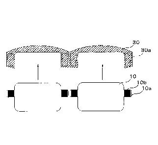
FIG. 6 is an explanatory view illustrating connection
between electrode pads disposed on the electrochromic element of
FIG. 4 and connecting members disposed on a frame.
As illustrated in FIG. 6, the electrode pads 10b disposed on
the protrusions 10a of the electrochromic element 10 and the
connecting members 30a disposed on the frame 30 are fitted
together in the direction of the arrows in FIG. 6 to electrically
connect. Note that, the connecting members 30a are connected
to a power source not illustrated in FIG. 6.
FIG. 7A is a schematic view of a cross-section illustrating a
state where an electrode pad is disposed in the electrochromic
element of FIG. 4. FIG. 7B is a schematic view of a cross-section
illustrating a state where a connecting member is connected to
38
CA 03008595 2018-06-14
,
,
the electrode pad of the electrochromic element of FIG. 7A.
As illustrated in FIG. 7B, the electrode pad 10b is fitted
with the connecting member 30a disposed on the frame 30 to
electrically connect the electrode pad 10b to the connecting
member 30a. As a result, a contact area becomes large and
electrical connection having excellent durability can be obtained
compared to an exposed electrode formed on an inclined plane
part of the lens edge according to the art as illustrated in FIG. 8.
Examples
The present invention will be described in more detail by
ways of the following Examples, but the present invention should
not be construed as being limited to these Examples.
(Example 1)
<Production of electrochromic element>
-Production of first substrate-
As a first substrate, an oval polycarbonate substrate
having a major axis length of 80 mm, a minor axis length of 55
mm, and an average thickness of 0.5 mm was produced.
-Formation of first electrode layer-
As a first electrode layer, an ITO film having an average
thickness of 100 nm was formed on the first substrate by
sputtering.
-Formation of electrochromic layer-
39
CA 03008595 2018-06-14
A titanium oxide nandpartide dispersion liquid (SP-210,
available from Showa Denko Ceramics Co., Ltd., average particle
diameter: 20 nm) was applied onto a surface of the obtained first
electrode layer by spin coating, followed by annealing for 5
minutes at 120 C, to thereby form a titanium oxide particle film
(nano structure semiconductor material) having an average
thickness of 1.0 pm.
Next, a 2,2,3,3,-tetrafluoropropanol solution including
1.5% by mass of a dipyridine-based compound represented by
Structural Formula (1) below as an electrochromic compound was
applied by spin coating, followed by annealing for 10 minutes at
120 C, to thereby form an electrochromic layer on which the
titanium oxide particles were born.
[Structural Formula (1)]
0 + / / ) i-7
¨CN
P ______________________________ \ __ //
He
2C1"
-Formation of insulating inorganic-particle layer-
A Si02 particle dispersion liquid (concentration of silica
solid content: 24.8% by mass, polyvinyl alcohol: 1.2% by mass,
and water: 74.0% by mass) where primary particles of the Si02
particles had a number average particle diameter of 20 nm was
CA 03008595 2018-06-14
applied onto the obtained electrochromic layer by spin coating, to
thereby form an insulating inorganic-particle layer having an
average thickness of 2 pm.
-Production of second substrate-
As a second substrate, a polycarbonate substrate identical
to the first substrate was produced.
-Formation of second electrode layer-
As a second electrode layer, an ITO film having an average
thickness of 100 nm was formed on the second substrate by
sputtering.
-Formation of electrolyte-
Onto a surface of the insulating inorganic-particle layer, a
solution in which polyethylene diacrylate, a photopolymerization
initiator (IRGACURE (registered trademark) 184, available from
BASF), an electrolyte (1-ethyl-3-methylimidazolium salt) were
mixed at 100:5:40 (mass ratio) was applied, and the surface of the
insulating inorganic-particle layer was bonded to a surface of the
substrate to which the second electrode layer had been formed,
followed by UV curing, to thereby form an electrolyte between the
first electrode layer and the second electrode layer.
-Formation of protective layer-
An ultraviolet ray-curable adhesive (KAYARAD R-604,
available from Nippon Kayaku Co., Ltd.) was dripped on side
surfaces of a bonded body where the insulating inorganic-particle
41
CA 03008595 2018-06-14
layer and the second electrode layer were bonded together, and
the ultraviolet ray-curable adhesive was cured by irradiation of
ultraviolet rays, to thereby form a protective layer having an
average thickness of 3 m.
As described above, an electrochromic element before
thermoforming illustrated in FIG. 2C was produced.
<Production of electrochromic device>
The obtained electrochromic element before
thermoforming was subjected to lens shape processing to fit with
a shape of a desired frame, to form protrusions each having a
width of 3 mm and a length of 5 mm on both sides of the
electrochromic element along a major axis direction. Silver
paste (DOTITE, available from FUJIKURA KASEI CO., LTD.)
serving as a conductive adhesive was applied to each of the
protrusions using a brush or a toothpick, a copper foil was wound
around each of the protrusions, and then the silver paste was
cured for 15 minutes at 60 C to electrically connect an edge of the
first electrode layer or the second electrode layer exposed by
scraping the protective layer through the lens shape processing to
the copper foil with the silver paste, to thereby produce electrode
pads. Next, the electrochromic element was formed into a lens
by thermoforming, and then the electrochromic element was
mounted in a rim of a frame as illustrated in FIG. 7B. As a
result, the electrode pads and connecting members disposed on
42
CA 03008595 2018-06-14
the frame were electrically connected to thereby produce
Electrochromic Device 1.
Voltage of ¨3.5 V was applied between the first electrode
layer and the second electrode layer of Electrochromic Device 1
obtained in a manner that the first electrode layer was to be a
negative electrode. As a result, Electrochromic Device 1 colored
in magenta derived from the electrochromic compound
represented by Structural Formula (1) above, and light
adjustment of Electrochromic Device 1 was achieved.
<Evaluation of durability of electrical connection>
The operation of opening temples of Electrochromic Device
1 and the operation of closing the temples were repetitively
performed by rotating hinges, and whether light adjustment
could be performed was confirmed after performing the
operations 100 times, after 1,000 times, and after 2,000 times.
As a result, light adjustment could be performed after 100 times
and 1,000 times without any problem, but light adjustment could
not be performed after 2,000 times due to a conduction failure.
(Example 2)
<Production of electrochromic element>
-Production of first substrate-
As a first substrate, a circular urethane lens having a
diameter of 75 mm and an average thickness of 2 mm was
prepared.
43
CA 03008595 2018-06-14
=
-Formation of first electrode layer,
As a first electrode layer, an ITO film having an average
thickness of 100 nm was formed on the obtained lens by
sputtering.
-Formation of electrochromic layer-
A titanium oxide nanoparticle dispersion liquid (SP-210,
available from Showa Denko Ceramics Co., Ltd., average particle
diameter: 20 nm) was applied onto a surface of the obtained
electrode layer by spin coating, followed by annealing for 5
minutes at 120 C, to thereby form a titanium oxide particle film
(nano structure semiconductor material) having an average
thickness of 1.0 pm.
A 2,2,3,3-tetrafluoropropanol solution including 1.5% by
mass of a dipyridine-based compound represented by Structural
Formula (1) above as an electrochromic compound was applied by
spin coating, followed by annealing for 10 minutes at 120 C to
allow the titanium oxide particle film to bear (adsorb) the
electrochromic compound to thereby form an electrochromic layer.
-Formation of insulating porous layer and second electrode layer
having through holes-
A Si02 particle dispersion liquid (concentration of silica
solid content: 24.8% by mass, polyvinyl alcohol: 1.2% by mass,
and water: 74.0% by mass) where primary particles of the Si02
particles had a number average particle diameter of 20 nm was
44
CA 03008595 2018-06-14
,
applied onto the obtained elatrochromic layer by spin coating, to
thereby form an insulating inorganic-particle layer having an
average thickness of 2 pm.
Moreover, a Si02 particle dispersion liquid (concentration
of silica solid content: 1% by mass and 2-propanol: 99% by mass)
where primary particles of the Si02 particles had a number
average particle diameter of 450 nm was applied by spin coating
to form a mask for forming through holes. On the mask for
forming through holes, a ZnS¨Si02 (molar ratio = 8/2) layer
having an average thickness of 40 nm was formed on the mask for
forming through holes by sputtering. On the ZnS¨Si02 (molar
ratio = 8/2) layer, moreover, an ITO film having an average
thickness of 100 nm was formed as the second electrode layer by
sputtering.
Thereafter, ultrasonic-wave irradiation was performed in
2-propanol to remove the Si02 particles where primary particles
of the Si02 particles had the number average particle diameter of
450 nm, to thereby form a ZnS¨Si02 (molar ratio = 8/2) layer
having a large number of pores piecing through in the thickness
direction and the second electrode layer having through holes.
-Formation of deterioration prevention layer-
A titanium oxide nanoparticle dispersion liquid (SP-210,
available from Showa Denko Ceramics Co., Ltd., average particle
diameter: 20 nm) was applied onto a surface of the obtained
CA 03008595 2018-06-14
second electrode layer having throiugh holes by spin coating,
followed by annealing for 5 minutes at 120 C, to thereby form a
titanium oxide particle film (nano structure semiconductor
material) having an average thickness of 1.0 pm.
Tetrabutylammonium perchlorate serving as an electrolyte,
and dimethyl sulfoxide and polyethylene glycol serving as
solvents were mixed at 12:54:60 (mass ratio) to thereby prepare
an electrolyte solution. The electrochromic element in which up
to the deterioration prevention layer had been formed was dipped
in the electrolyte solution, followed by drying on a hot plate of
120 C, to thereby form an electrolyte.
-Formation of protective layer-
An ultraviolet ray-curable adhesive (SD-17, available from
DIC Corporation) was applied onto the obtained deterioration
prevention layer by spin coating, followed by ultraviolet-light
irradiation to cure the adhesive, to thereby form a protective
layer having an average thickness of 3 pm.
As described above, Electrochromic Element 2 was
produced.
<Production of electrochromic device>
Lens shape processing was performed, electrode pads were
formed on the lenses, and the lenses were mounted in a frame to
produce Electrochromic Device 2 in the same manner as in
Example 1, except that Electrochromic Element 1 was replaced
46
CA 03008595 2018-06-14
with Electrochromic Element 2. An evaluation was performed in
the same manner as in Example 1.
As a result, it was confirmed that light adjustment could
be performed without any problem after 100 times and after 1,000
times similarly to Example 1, but a conduction failure occurred
when confirmed after 2,000 times.
(Example 3)
An electrochromic device of Example 3 was produced in the
same manner as in Example 1, except that flat springs were used
as connecting members each of which nipped the electrode pad,
and an evaluation was performed in the same manner as in
Example 1.
As a result, light adjustment could be performed without
any problem even after 2,000 times. A reason thereof was
assumed that the flat spring was in contact with the copper foil of
the electrode pad even when the electrochromic element was
moved inside the rim of the frame because the flat spring nipped
the electrode pad and hence electrical connection could be
securely obtained.
(Comparative Example 1)
An electrochromic device of Comparative Example 1 was
produced in the same manner as in Example 1, except that, as
illustrated in FIG. 8, the periphery of the electrochromic element
33 was subjected to lens edging, and the electrode layer 41
47
CA 03008595 2018-06-14
exposed on the inclined surfdce of the lens edge and a connecting
member 52 of the frame were electrically connected via
anisotropic conductive rubber 51. An evaluation was performed
in the same manner as in Example 1.
As a result, a conduction failure occurred when confirmed
after 100 times.
For example, embodiments of the present invention are as
follows.
<1> An electrochromic device including:
an electrochromic element including a protrusion on a periphery
of the electrochromic element; and
a frame holding the electrochromic element,
wherein the protrusion includes an electrode pad, and
the frame includes a connecting member configured to electrically
connect to the electrode pad.
<2> The electrochromic device according to <1>,
wherein the electrochromic element includes a first substrate, a
first electrode layer, an electrochromic layer, an insulating
inorganic-particle layer, a second electrode layer, and a second
substrate in the order as mentioned, and
an electrolyte is disposed between first electrode layer and the
second electrode layer.
<3> The electrochromic device according to <1>,
wherein the electrochromic element includes a first substrate, a
48
CA 03008595 2018-06-14
first electrode layer, an electrochtomic layer, an insulating
porous layer, a second electrode layer having through holes, and a
deterioration prevention layer in the order as mentioned, and
an electrolyte is disposed between the first electrode layer and
the deterioration prevention layer.
<4> The electrochromic device according to any one of <1> to
<3>,
wherein the connecting member is an elastic material that can
press against the electrode pad.
<5> The electrochromic device according to <4>,
wherein the elastic material is a flat spring.
<6> The electrochromic device according to any one of <2> to
<5>,
wherein an edge of the first electrode layer or the second
electrode layer is electrically connected to the electrode pad with
a conductive adhesive.
<7> The electrochromic device according to any one of <1> to
<6>,
wherein the electrode pad is a metal foil.
<8> The electrochromic device according to <7>,
wherein the metal foil is wound around the protrusion.
<9> The electrochromic device according to <7> or <8>,
wherein the metal foil is a copper foil.
<10> The electrochromic device according to any one of <6> to
49
CA 03008595 2018-06-14
<9>, ,
wherein the conductive adhesive is silver paste.
<11> The electrochromic device according to any one of <2> to
<10>,
wherein the first electrode layer, or the second electrode layer, or
both of the first electrode layer and the second electrode layer is
tin-doped indium oxide.
<12> The electrochromic device according to any one of <2> to
<11>,
wherein the electrochromic layer includes an organic
electrochromic compound on which conductive particles or
semiconductive particles are born.
<13> The electrochromic device according to <12>,
wherein the conductive particles or the semicoductive particles
are metal oxide.
<14> The electrochromic device according to <13>,
wherein the metal oxide is titanium oxide.
<15> The electrochromic device according to any one of <2> to
<14>,
wherein an average thickness of the electrochromic layer is 0.2
pm or greater but 5.0 pm or less.
<16> The electrochromic device according to any one of <2> to
<15>,
wherein the electrochromic element further includes a protective
CA 03008595 2018-06-14
= ,
layer.
<17> The electrochromic device according to <16>,
wherein an average thickness of the protective layer is 0.5 pm or
greater but 10 pm or less.
<18> The electrochromic device according to any one of <1> to
<17>,
wherein the electrochromic element is in the shape of a lens.
<19> The electrochromic device according to any one of <2> to
<18>,
wherein the first substrate is a lens.
<20> The electrochromic device according to any one of <1> to
<19>,
wherein the electrochromic device is a pair of electrochromic
light-adjusting spectacles.
The electrochromic device according to any one of <1> to
<20> can solve the above-described various problems existing in
the art and can achieve the object of the present invention.
Description of the Reference Numeral
10: electrochromic element
10a: protrusion
10b: electrode pad
11: first substrate
12: first electrode layer
51
CA 03008595 2018-06-14
13: electrochromic layer
14: insulating inorganic-particle layer
16: second electrode layer
17: second substrate
21: insulating porous layer
22: deterioration prevention layer
23: protective layer
30: frame
30a: connecting member
io 100: electrochromic device
52