Note: Descriptions are shown in the official language in which they were submitted.
CA 03009045 2018-06-18
WO 2017/105485 PCT/US2015/066633
GROUND FAULT CIRCUIT INTERRUPTER (GFCI)
SYSTEM AND METHOD
BACKGROUND
[0001] The present invention relates generally to switched electrical
devices. More
particularly, the present invention is directed to circuit interrupting
devices, such as ground fault
circuit interrupter (GFCI) devices, that switch to a "tripped" or unlatched
state from a "reset" or
latched state when one or more conditions is detected. Such devices consistent
with
embodiments of the invention disclosed herein are more reliable and have a
longer life
expectancy than previously known GFCI devices.
[0002] GFCI devices having contacts that are biased toward the open
position require a
latching mechanism for setting and holding the contacts in a closed position.
Likewise, switched
electrical devices having contacts that are biased toward the closed position
require a latching
mechanism for setting and holding the contacts in an open position. Examples
of conventional
types of devices include devices of the circuit interrupting type, such as
circuit breakers, arc fault
interrupters, and GFCIs, to name a few.
[0003] As a result of GFCI devices being relatively small, when in the open
position, the
contacts may still be relatively close to each other. This may lead to slow
plasma extinguishing,
electrical arching, and relatively slow disconnections (e.g., opening) of the
contacts. These
conditions can result in high failure rates for the device due to residue
build-up on the contacts
which can lead to longer disconnect times and possibly permanent failure.
SUMMARY
[0004] The present invention solves such issues, by providing, in one
embodiment, a wiring
device including a face terminal for electrically connecting to an external
load; a line terminal for
electrically connecting to an external power supply; a load terminal for
electrically connecting to
a second external load; a face contact electrically connected to the face
terminal; one or more
line contact arms electrically connected to the line terminal; and one or more
load contact arms
electrically connected to the load terminal. Each line contact arm having an
upper line contact
located on a bent portion of the line contact arm, and a lower line contact
located on a
1
CA 03009045 2018-06-18
WO 2017/105485 PCT/US2015/066633
substantially straight portion of the line contact arm. Each load contact arm
having a load
contact located on a bent portion of the load contact arm. Wherein, the face
contact and the
upper line contact are electrically connected, and the lower line contact and
the load contact are
electrically connected, when the wiring device in is a closed position, and
the face contact and
the upper line contact are electrically disconnected, and the lower line
contact and the load
contact are electrically disconnected when the wiring device is in an open
position.
[0005] In another embodiment the invention provides a wiring device
including a face
contact; one or more line contact arms; one or more load contact arms; and a
fault detection
circuit. The one or more line contact arms having an upper line contact
located on a bent portion
of the line contact arm, and a lower line contact located on a substantially
straight portion of the
line contact arm. The one or more load contact arms having a load contact
located on a bent
portion of the load contact arm. The fault detection circuit that detects a
fault condition in said
wiring device and generates a fault detection signal when said fault condition
is detected,
wherein said fault detection signal electrically disconnects the face contact
from the upper line
contact and the lower line contact from the load contact.
[0006] In yet another embodiment the invention provides a method of
operating a wiring
device. The method including providing a face contact; providing one or more
line contact arms;
and providing one or more load contact arms. Each line contact arm having an
upper line contact
located on a bent portion of the line contact arm, and a lower line contact
located on a
substantially straight portion of the line contact arm. Each load contact arm
having a load
contact located on a bent portion of the load contact arm. The method further
including
electrically connecting the face contact and the upper line contact; and
electrically connecting the
lower line contact and the load contact.
[0007] Other aspects of the invention will become apparent by consideration
of the detailed
description and accompanying drawings.
BRIEF DESCRIPTION OF THE DRAWINGS
[0008] FIG. 1 is a side elevation view of a self-testing GFCI receptacle
device in accordance
with an exemplary embodiment of the present invention.
2
CA 03009045 2018-06-18
WO 2017/105485 PCT/US2015/066633
[0009] FIG. 2 is a side elevation view of the self-testing GFCI receptacle
shown in FIG. 1
with the front cover of the housing removed.
[0010] FIG. 3 is a side elevation view of a core assembly of the self-
testing GFCI receptacle
device shown in FIG. 1.
[0011] FIG. 4 is a side view of a line contact arm and a load contact arm
of the GFCI
receptacle shown in FIG. 1 in an open position.
[0012] FIG. 5 is a side view of a line contact arm and a load contact arm
of the GFCI
receptacle shown in FIG. 1 in a closed position.
[0013] FIGS. 6A-6D is a schematic of an exemplary circuit consistent with
an exemplary
embodiment of the present invention.
DETAILED DESCRIPTION
[0014] Before any embodiments of the invention are explained in detail, it
is to be
understood that the invention is not limited in its application to the details
of construction and the
arrangement of components set forth in the following description or
illustrated in the following
drawings. The invention is capable of other embodiments and of being practiced
or carried out
in various ways.
[0015] FIG. 1 illustrates a perspective view of a GFCI receptacle 10
according to one
embodiment of the invention. The GFCI receptacle 10 includes a front cover 12
having a duplex
outlet face 14 with a phase opening 16, a neutral opening 18, and a ground
opening 20. The face
14 further has opening 22, accommodating a RESET button 24, an adjacent
opening 24,
accommodating a TEST button 28, and six respective circular openings 30-15. In
some
embodiments, openings 30 and 33 accommodate two respective indicators, such as
but not
limited to, various colored light-emitting diodes (LEDs). In some embodiments,
openings 32
and 34 accommodate respective bright LEDs used, for example, as a nightlight.
In some
embodiments, opening 31 accommodates a photoconductive photocell used, for
example, to
control the nightlight LEDs. In some embodiments, opening 35 provides access
to a set screw
for adjusting a photocell device in accordance with this, as well as other,
embodiments.
3
CA 03009045 2018-06-18
WO 2017/105485 PCT/US2015/066633
[0016] The GFCI receptacle 10 further includes a rear cover 36 secured to
the front cover 12
by eight fasteners 38 (four fasteners 38 are shown in FIG. 1, while the other
four fasteners 38 are
obstructed from view). In some embodiments, the fasteners 38 include a barbed
post 50 on the
front cover 12 and a corresponding resilient hoop 52 on the rear cover 36,
similar to that which is
described in detail in U.S. Pat. No. 6,398,594, the entire contents of which
are incorporated
herein by reference for all that is taught. A ground yoke/bridge assembly 40
includes standard
mounting ears 42 protruding from the ends of the GFCI receptacle 10.
[0017] FIG. 2 illustrates a perspective view of the GFCI receptacle 10 with
the front cover 12
removed in order to expose manifold 126. Manifold 126 provides support for a
printed circuit
board 390 and the yoke/bridge assembly 40. According to one embodiment,
manifold 126
includes four dovetail interconnects 130 that mate with corresponding cavities
132 along an
upper edge of the rear cover 36. One dovetail-cavity pair is provided on each
of the four sides of
manifold 126 and rear cover 36, respectively.
[0018] FIG. 3 is a side elevation view of a core assembly 80 according to
one embodiment.
Core assembly 80 includes a circuit board 82 that supports most of the working
components of
the receptacle, including the circuit shown in FIGS. 6A-6D, which are referred
to collectively
herein as FIG. 6, as well as a sense transformer 84 and a grounded neutral
transformer 85 (not
shown). Line contact arms 94, 96 pass through transformers 84, 85 with an
insulating separator
98 there between. Line contact arms 94, 96 are cantilevered, their respective
distal ends carrying
phase and neutral line contacts 102, 104. Load contact arms 98, 100 are also
cantilevered with
their respective distal ends carrying phase and neutral load contacts 101,
103. The resiliency of
the cantilevered contact arms biases the line contacts 102, 104 and load
contacts 101, 103 away
from each other. Load contact arms 98, 103 rest on a movable contact carriage
106, made of
insulating (preferably thermoplastic) material.
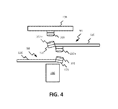
[0019] FIG. 4 is a side view of the line contact arm 94 and the load
contact arm 98 in an
open position, according to one embodiment. FIG. 4 further illustrates the
load contact 101 (e.g.,
the phase load contact or neutral load contact), the line contact 102 (e.g.,
the phase line contact
or the neutral line contact), the movable contact carriage, or latch housing,
106, a face 108, and a
face contact 109 (e.g., a phase face contact or a neutral face contact). In
some embodiments, the
4
CA 03009045 2018-06-18
WO 2017/105485 PCT/US2015/066633
face 108 is the bottom portion of the manifold 126. Although not illustrated
in FIG. 4, line
contact arm 96, load contact arm 100, load contact 103 (e.g., the phase load
contact or neutral
load contact), and line contact 104 (e.g., the phase line contact or the
neutral line contact), are
constructed in a similar fashion as illustrated in FIGS. 4 and 5, and
explained below. Also, it is
noted that according to various embodiments the contact and contact arm
configuration shown
and described in regard to FIGS. 4 and 5 is also provided in the devices shown
and described in
regard to FIGS. 1-3.
[0020] The line contact arm 94 includes a first straight, or substantially
straight, portion 110
and a first bent portion 115. The first straight portion 110 includes a lower
line contact 102a,
while the first bent portion 115 includes an upper line contact 102b. In some
embodiments, the
line contact arm 94 is bent at an angle of approximately three degrees,
although, the line contact
arm may be bent at an angle ranging from approximately three degrees to
approximately six
degrees. The lower line contact 102a may be coupled to the line contact arm 94
by inserting a
hole prior to the upper line contact 102b. In some embodiments, the lower line
contact 102a and
the upper line contact 102b are coupled to the line contact arm 94 via
riveting.
[0021] The load contact arm 98 includes a second straight, or substantially
straight, portion
120 and a second bent portion 125. The second bent portion 125 having the load
contact 101. In
some embodiments, the load contact arm 98 is bent at an angle of approximately
three degrees to
approximately six degrees. In some embodiments, the load contact 101 is
coupled to the load
contact arm 98 via riveting.
[0022] FIG. 5 is a side view of the line contact arm 94 and the load
contact arm 98 in a
closed position, according to the embodiment of FIG. 4. The line contact arm
94 is bent down
such that, when in the closed position, the upper line contact 102b is in a
substantially flat
contact with the face contact 109. Additionally, the load contact arm 98 is
bent down such that,
when in the closed position, the load contact 101 is in substantially flat
contact with the lower
line contact 102a.
[0023] In operation, when the line contact arms 94, 96 and load contact
arms 98, 100 go
from the closed position to an open position, or from the open position to the
closed position, a
wiping action is performed. Additionally, a moment of force is added by the
bent portions of the
CA 03009045 2018-06-18
WO 2017/105485 PCT/US2015/066633
contact arms of the when the line contact arms 94, 96 and load contact arms
98, 100 are in the
reset condition. This wiping action and added moment of force allows for the
contacts to float
and maintain connection, even in the case of movement of the GFCI receptacle
10. The wiping
action, the added moment of force, and the bent portions, result in relatively
large openings
between the contacts, relatively fast openings between the contacts when the
device is tripped.
The relatively large openings and relatively fast openings result in
relatively fast plasma
extinguishing which, among other things, reduces the possibility for arcing.
[0024] The relatively large openings, or space, between the contacts
additionally allow for
cooler operation of the GFCI receptacle 10 by allowing more air and surface
cooling. The
relatively large openings also prevent arcing between the contacts, which can
occur in high
voltage operation or if the brush arms lose spring forces. In some
embodiments, when in the
open position the contacts are approximately 0.060" away from each other. The
bent portions of
the line contact arms 94, 96 and load contact arms 98, 100 further move the
contacts off of the
movable contact carriage 106, thereby preventing any potential melting.
[0025] FIG. 6 (FIGS. 6A-6D) is a schematic drawing of an electrical circuit
in accordance
with one embodiment of the invention. The circuit shown in FIG. 6, or various
sub-circuits
thereof, can be implemented in a variety electrical wiring devices, however,
for purposes of
description here the circuit of FIG. 6 is discussed in conjunction with its
use in the GFCI
receptacle device shown in FIGS. 1-5.
[0026] The circuit of FIG. 6 includes phase line terminal 326 and neutral
line terminal 328
for electrical connection to an AC power source (not shown), such as a 60-
hertz, 120 volt rms
power source as used in the United States for mains power. The circuit of FIG.
6 and the
software resident on and implemented therewith, can be modified to accommodate
other power
delivery systems as well. Such modifications and the resultant circuit and
wiring device in
which the circuit and software are would ultimately be used are contemplated
by the inventor
and considered to be within the spirit and scope of the invention described
herein. For example,
power delivery systems that use different voltages and frequencies are within
the scope of the
invention.
6
CA 03009045 2018-06-18
WO 2017/105485 PCT/US2015/066633
[0027] Referring to FIG. 6, phase conductor 330 and neutral conductor 332
are respectively
connected to the line terminals and each pass through sense transformer 334
and grounded
neutral transformer 336, which are part of a detection circuit described
below. By way of
example, line terminals correspond to input terminal screws 326, 328 in FIG. 1
above and line
conductors 330, 332 represent line contact arms 94, 96, respectively, as
described above with
respect to FIG. 3. Each of line conductors 330, 332 has a respective fixed end
connected to the
line terminals and each includes a respective movable contact, e.g. contacts
102, 104 from the
embodiment described above. Face phase and face neutral conductors 338, 340,
respectively,
include electrical contacts, e.g., contacts 109 from the embodiment described
above, fixed
thereto. The face conductors 338, 340 are electrically connected to and, in
the embodiment
shown are integral with, respective face terminals 342, 344, to which plug
blades from a load
device (not shown), such as an electrical appliance, would be connected when
the electrical
receptacle device is in use.
[0028] The circuit shown in FIG. 6 according to this embodiment also
includes optional load
phase and load neutral terminals 346, 348, respectively, which electrically
connect to a
downstream load (not shown), such as one or more additional receptacle
devices. Load terminals
346, 348 are respectively connected to cantilevered load conductors 277, 278,
each of which
includes movable load contacts 101, 103 (FIGS. 4 and 5), at its distal end.
The load contacts
101, 103 are disposed below respective line contacts 102, 104 (FIGS. 4 and 5)
and face contacts
109 (FIGS. 4 and 5) and are coaxial with them such that when the line
conductors are moved
toward the load and face conductors, the three sets of contacts mate and are
electrically
connected together. When the device is in this condition it is said to be
"reset" or in the reset
state.
The Detector Circuit
[0029] With continued reference to FIG. 6, detector circuit 352 includes
transformers 334,
336 as well as a GFCI integrated circuit device (GFCI IC), 350. In accordance
with the present
embodiment GFCI IC 350 is the well-known 4141 device, such as an RV4141 device
made by
Fairchild Semiconductor Corporation. Other GFCI IC devices could also be used
in the circuit
7
CA 03009045 2018-06-18
WO 2017/105485 PCT/US2015/066633
of FIG. 6 instead of the 4141 and such a modification is within the spirit and
scope of the
invention.
[0030] GFCI IC device 350 receives electrical signals from various other
circuit components,
including transformers 334, 336, and detects one or more kinds of faults, such
as a real fault, a
simulated fault or self-test ground fault, as well as a real or simulated
grounded neutral fault. For
example, when a sufficient current imbalance in line conductors 330, 332
occurs, a net current
flows through the transformers 334, 336, causing a magnetic flux to be created
about at least
transformer 334. This magnetic flux results in electrical current being
induced on conductor 333,
which is wound around sense transformer 334. Respective ends of conductor 333
are connected
to the positive and negative inputs to the sense amplifier of GFCI IC device
350 at input ports V-
REF and VFB, respectively. The induced current on conductor 333 causes a
voltage difference
at the inputs to the sense amplifier of GFCI IC 350. When the voltage
difference exceeds a
predetermined threshold value, a detection signal is generated at one or more
of outputs of GFCI
IC 350, such as the SCR trigger signal output port (SCR OUT). The threshold
value used by
GFCI IC 350 is determined by the effective resistance connected between the op-
amp output
(OP OUT) and the positive input to the sense amplifier (VFB).
[0031] The current imbalance on line conductors 330, 332 results from
either a real ground
fault, a simulated ground fault or a self-test ground fault. A simulated
ground fault is generated
when test switch 354 in FIG. 6 closes, which occurs when TEST button 28 (FIG.
1) is pressed.
As described in further detail below, a self-test fault occurs when auto-
monitoring circuit 370
initiates an auto-monitoring test sequence that includes an electrical current
being generated on
independent conductor 356.
[0032] According to the present embodiment, when test switch 354 closes,
some of the
current flowing in line conductors 330, 332 and load conductors 338, 340 is
diverted from the
phase face conductor 338 (and phase load conductor 277 when the device is in
the reset state)
around sense transformer 334 and through resistor 358 to neutral line
conductor 332. By
diverting some of the current through resistor 358 in this manner, an
imbalance is created in the
current flowing through conductor 330 and the current flowing in the opposite
direction through
conductor 332. When the current imbalance, i.e., the net current flowing
through the conductors
8
CA 03009045 2018-06-18
WO 2017/105485 PCT/US2015/066633
passing through the sense transformer, exceeds a threshold value, for instance
4-5 milliamps, this
simulated ground fault is detected by detector circuit 352 and the SCR output
of GFCI IC 350
(SCR OUT) is activated.
[0033] When the SCR output of GFCI IC 350 is activated, the gate of SCR 360
is turned ON
allowing current to flow from the phase line conductor 330 through diode 359
and SCR 360.
The current flowing through SCR 360 turns ON the gate of SCR 361 and SCR 369.
When SCR
361 is turned ON, current flows from phase line conductor 330 through
secondary coil 363 of
dual-coil solenoid 362, fuse 365, diode 367 and SCR 361. Further, when SCR 369
is turned ON,
current flows from phase line conductor 330 through primary coil 364 of dual-
coil solenoid 362,
fuse 372, diode 374 and SCR 369. The current flowing through both coils 363,
364 generates a
magnetic field that moves an armature within solenoid 362. When the solenoid
armature moves,
it unlatches a contact carriage, (e.g., 106 in FIG. 3) which is part of
interrupting device 315, and
the carriage drops under the natural bias of line conductors 330, 332, that
is, away from the face
conductors 338, 340 and load conductors 277, 278. The device is now said to be
"tripped," as a
result of the successful manual simulated fault test sequence, and the device
will not deliver
power to a load until it is reset. The time it takes from the instant switch
354 closes until the
device is tripped and current no longer flows from phase line conductor 330 to
either the face
and load conductors and through solenoid coils 363, 364, is so short that
fuses 365, 372 remain
intact.
Manual Testing Via the Reset Operation
[0034] With continued reference to FIG. 6, closing reset switch 300, e.g.,
by pressing
RESET button 24 (FIG. 1), also initiates a test operation. Specifically, when
reset switch 300
closes, a voltage supply output, VS, of GFCI IC 350 is electrically connected
to the gate of SCR
360 through conductor 308, thus, turning ON SCR 360. When SCR 360 is turned
ON, current is
drawn from line conductor 330 through diode 359 and SCR 360 and ultimately to
ground.
Similar to when SCR 360 is turned ON by pressing the TEST button, as discussed
previously,
turning ON SCR 360 by pressing the RESET button results in SCR 361 and SCR 369
also being
turned ON and current flowing through solenoid coils 363, 364. The current
flowing through
coils 363, 364 of solenoid 362 generates a magnetic field at the solenoid and
the armature within
9
CA 03009045 2018-06-18
WO 2017/105485 PCT/US2015/066633
the solenoid is actuated and moves. Under typical, e.g., non-test, conditions,
the armature is
actuated in this manner to trip the device, such as when an actual fault
occurs.
[0035] When reset switch 300 closes, however, the device is likely already
in the tripped
condition, i.e., the contacts of the line, face and load conductors are
electrically isolated. That is,
the RESET button is usually pressed to re-latch the contact carriage and bring
the line, face and
load contacts back into electrical contact (illustrated in FIG. 5) after the
device has tripped. If
the armature of solenoid 362 fails to fire when the RESET button is pressed,
and the reset
mechanism, including the contact carriage, fails to engage the reset plunger
on its return after the
RESET button is released, the device will not reset. Accordingly, if, for
example, the device has
not been wired to the AC power lines, or it has been mis-wired, that is, the
device has been wired
with the AC power not connected to the line terminals, 326, 328, no power is
applied to the
GFCI IC 350. If no power is applied to GFCI IC 350, the gate of SCR 360 cannot
be driven,
either by the SCR output of GFCI IC 350 or when the REST button is pressed.
Under this
condition the device will not be able to be reset. The mis-wire condition is
prevented in
accordance with a wiring device consistent with the present embodiment by
ensuring the device
is shipped to the user in the tripped condition. Because the device cannot be
reset until AC
power is properly applied to the line terminals, the mis-wire condition is
prevented.
The Auto-Monitoring Circuit
[0036] With continued reference to the exemplary circuit schematic shown in
FIG. 6, auto-
monitoring circuit 370 includes a programmable device 301. Programmable device
301 can be
any suitable programmable device, such as a microprocessor or a
microcontroller, which can be
programmed to implement the auto-monitoring routine as explained in detail
below. For
example, according to the embodiment shown in FIG. 6, programmable device 301
is
implemented by an ATMEL.TM. microcontroller from the ATtiny 10 family. It
could also be
implemented by a Microchip microcontroller such as a PIC10F204/206.
[0037] According to one exemplary auto-monitoring, or automatic self-
testing, routine in
accordance with the embodiment shown in FIG. 6, microcontroller 301 initiates
the auto-
monitoring routine approximately every three (3) seconds by setting a software
auto-monitoring
test flag. The auto-monitoring test flag initiates the auto-monitoring routine
within the circuit
CA 03009045 2018-06-18
WO 2017/105485 PCT/US2015/066633
interrupting device and confirms that the device is operating properly or,
under certain
circumstances, determines that the circuit interrupting device has reached its
end-of-life (EOL).
When the auto-monitoring routine runs with a positive, i.e., successful,
result, the auto-
monitoring circuit enters a hibernation state until microcontroller 301 sets
the test flag again and
initiates another auto-monitoring routine.
[0038] If the auto-monitoring routine runs with a negative result, e.g., it
cannot be
determined that the circuit interrupting device is functioning properly or it
determines that it is,
in fact, not operating properly, a failure counter is incremented and
microcontroller 301 initiates
another auto-monitoring routine when instructed by the software program stored
in memory
within the device. In addition to the failure count being incremented, a
temporary indication of
the failure is also provided. For example, according to the present
embodiment, when such a
failure occurs, I/0 port GPO of microcontroller 301 is controlled to be an
output and light
emitting diode (LED) 376 is controlled to flash, e.g., one or more times, to
indicate the failure to
a user. If the failure counter reaches a predetermined value, i.e., the auto-
monitoring routine runs
with a negative result a certain number of times, the number being stored and
implemented in
software, the auto-monitoring routine invokes an end-of-life (EOL) sequence.
The EOL
sequence includes one or more of the following functions; (a) indicate that
EOL has been
reached, for example, by continuously flashing or illuminating an indicator
light and/or
generating an audible sound, (b) attempt to trip the device, (c) prevent an
attempt to reset the
device, (d) store the EOL event on non-volatile memory, e.g., in the event
there is a power
failure, and (e) clear the EOL condition when the device is powered down.
[0039] In accordance with this embodiment, when the auto-monitoring
software determines
it is time to run the auto-monitoring routine, i.e., based on the auto-monitor
timer, a stimulus
signal 302 is turned ON at I/O port GP1 of microcontroller 301. When the
stimulus signal is
turned ON, electrical current flows through resistor 303 and a voltage is
established at the base
of transistor 304, turning the transistor ON. When transistor 304 is turned
ON, current flows
from dc voltage supply 378 through resistor 305, which is, for example, a 3 k-
ohm resistor, and
continues through electrical conductor 356 and transistor 304 to ground.
Regarding dc voltage
source 378, according to the present embodiment the value of this voltage
source is designed to
be between 4.1 and 4.5 volts dc, but the value of this voltage supply can be
any other suitable
11
CA 03009045 2018-06-18
WO 2017/105485 PCT/US2015/066633
value as long as the value used is adequately taken into account for other
circuit functionality
described below.
[0040] According to this exemplary embodiment, electrical conductor 356 is
a wire, but it
could also be a conductive trace on a printed circuit board. Conductor 356 is
connected at one
end to resistor 305, traverses through sense transformer 334 and is looped
approximately ten (10)
times around the core of the transformer and connected at its other end to the
collector of
transistor 304. Thus, when the software auto-monitoring test flag is set in
microcontroller 301
and transistor 304 is turned ON, current flows through conductor 356 which
comprises an
independent conductor separate from phase line conductor 330 and neutral line
conductor 332,
which also traverse through the center of sense transformer 334.
[0041] If the circuit interrupting device according to the present
embodiment is functioning
properly, as current flows through conductor 356 and through the sense
transformer a magnetic
flux is generated at sense transformer 334. The flux generates a signal on
conductor 333 which
is detected by detection circuit 352, including GFCI IC device 350. In
accordance with this
embodiment, when device 350 detects the flux created at sense transformer 334,
a voltage level
is increased at one of the I/O ports of device 350, for example at the output
port labeled CAP in
FIG. 6, thus increasing the voltage on conductor 306.
[0042] According to this embodiment, capacitor 307 is connected between the
CAP I/O port
of microcontroller 301 and ground. As is known in the art, attaching a
capacitor directly
between the CAP output of a 4141 GFCI IC device and ground causes the SCR
trigger signal
(SCR OUT) output from GFCI IC device 350 to be delayed by a predetermined
period of time.
The amount of time the trigger signal is delayed is typically determined by
the value of the
capacitor. According to the present embodiment, however, capacitor 307 is not
connected
directly between the CAP output and ground. Instead, capacitor 307 is also
connected to the
ADC I/O port GPO of microcontroller 301 via a circuit path that includes diode
310 in series with
resistor 311, e.g., 3 M-Ohm, which completes a voltage divider circuit with
resistor 312, e.g., 1.5
M-Ohm. This additional circuitry connected to the capacitor at the CAP output
of GFCI IC
device 350 drains current from the delay capacitor.
12
CA 03009045 2018-06-18
WO 2017/105485 PCT/US2015/066633
[0043] By measuring the value of the signal at ADC I/O port (GPO) and
confirming it is
above a certain level, it can be determined whether or not the self-test fault
signal generated on
conductor 356 was properly detected by detection circuit 352 and it can
further be confirmed
whether GFCI IC device 350 is capable of generating the appropriate SCR
trigger signal. Also,
to avoid tripping the device during a self-test auto-monitoring fault, the
voltage at capacitor 307
is measured and proper self-test fault detection is confirmed before a drive
signal is output at
SCR OUT of GFCI IC device 350.
[0044] If the current drain on capacitor 307 is too high, GFCI IC device
350 may not operate
properly. For example, if as little as 3-4 microamps of current is drained
from capacitor 307,
grounded neutral conditions, which are also intended to be detected by GFCI IC
device 350, may
not be accurately detected, e.g., pursuant to UL requirements, because the SCR
trigger signal
(SCR OUT) will not fire within the necessary amount of time. According to the
present
embodiment, less than about 1.3 microamps, or about 5% of the specified delay
current for the
GFCI IC device 350, is drained for the ADC I/O port GPO of microcontroller
301. This small
current drain from capacitor 307 has no effect on the ability of the device to
properly detect real
ground faults and/or real grounded neutral faults.
[0045] According to this embodiment, approximately 50 nanoamps of current
is drawn off of
capacitor 307. Parallel resistors 311 and 312 connected to the ADC I/0 port
GPO of
microcontroller 301 create a 4.5 megaohm drain which limits the current pulled
from capacitor
307 to a maximum of 1.0 microamp. GFCI IC device 350 uses approximately 40
microamps of
current to generate the SCR trigger but microcontroller 301 only requires
approximately 50
nanamps to read the SCR trigger signal off of capacitor 307 before the SCR
trigger signal is
output from SCR OUT. Accordingly, by selecting the proper value for capacitor
307, in
conjunction with appropriate value selections for resistors 311 and 312, as
well as diode 310, it is
possible to maintain the correct delay for the SCR trigger signal (SCR OUT)
from GFCI IC
device 350 and use the ADC in microcontroller 301 to measure the signal at ADC
input (GPO) to
determine whether the test signal on conductor 356 has been properly detected
by detection
circuit 352.
13
CA 03009045 2018-06-18
WO 2017/105485 PCT/US2015/066633
[0046] It should also be noted that in the embodiment shown in FIG. 6, LED
376 is also
connected to ADC I/0 port (GPO) of microcontroller 301. Accordingly, whether
or not LED 376
is conducting or not will affect the drain on capacitor 307, as well as the
delay of the SCR trigger
signal and the ability of microcontroller 301 to properly measure the signal
output from the CAP
I/O port of GFCI IC device 350. Thus, in regard to the circuit shown in FIG.
6, LED 376 is
selected such that it does not turn ON and begin conducting during the time
microcontroller 301
is measuring the signal from the CAP output of GFCI IC device 350. For
example, LED 376 is
selected such that its turn-ON voltage is about 1.64 volts, or higher which,
according to the
circuit shown in FIG. 6, can be measured at I/O port GPO. Additionally, to
prevent any signal
adding to capacitor 307 when LED 376 is being driven, diode 310 is provided.
[0047] According to this embodiment, the circuit path that includes diode
310 and the
voltage divider, 311, 312, is connected to I/0 port GPO of microcontroller
301, which serves as
an input to an analog-to-digital converter (ADC) within microcontroller 301.
The ADC of
microcontroller 301 measures the increasing voltage established by the
charging action of
capacitor 307. When a predetermined voltage level is reached, microcontroller
301 turns OFF
the auto-monitoring stimulus signal 302 which, in turn, turns OFF transistor
304, stopping the
current flow on conductor 356 and, thus, the flux created at sense transformer
334. When this
occurs, it is determined by microcontroller 301 that a qualified auto-
monitoring event has
successfully passed and the auto-monitoring fail counter is decremented if the
present count is
greater than zero.
[0048] In other words, according to this embodiment an auto-monitoring
routine is repeated
by microcontroller 301 on a predetermined schedule. Based on the software
program stored in
memory within microcontroller 301, the auto-monitoring routine is run, as
desired, anywhere
from every few seconds to every month, etc. When the routine is initiated, the
flux created at
sense transformer 334 occurs in similar fashion to the manner in which flux
would be created if
either an actual ground fault had occurred or if a simulated ground fault had
been manually
generated, e.g., by pressing the TEST button as described above.
[0049] There is a difference; however, between an auto-monitoring (self-
test) fault generated
by the auto-monitoring routine and either an actual ground fault or a
simulated fault generated by
14
CA 03009045 2018-06-18
WO 2017/105485 PCT/US2015/066633
pressing the TEST button. When either an actual or simulated ground fault
occurs, a difference
in the current flowing in the phase and neutral conductors, 330 and 332,
respectively, should be
generated. That is, the current on conductor 330 should be different than the
current on
conductor 332. This differential current flowing through sense transformer 334
is detected by
GFCI IC device 350, which drives a signal on its SCR OUT I/O port to activate
the gate of SCR
360 and turn it ON. When SCR 360 turns ON, current is drawn through coils 363,
364 which
causes interrupting device 315 to trip, causing the contact carriage to drop
which, in turn, causes
the line, face and load contacts to separate from each other (as illustrated
in FIG. 4). Thus,
current is prevented from flowing through phase and neutral conductors 330,
332 to the phase
and neutral face terminals 342, 344, and the phase and neutral load terminals
346, 348,
respectively.
[0050] In comparison, when the auto-monitoring routine is performed in
accordance with the
present invention, no differential current is created on the phase and neutral
conductors 330, 332
and the interrupting device 315 is not tripped. Instead, during the auto-
monitoring routine, the
flux generated at sense transformer 334 is a result of current flowing through
conductor 356,
which is electrically separated from phase and neutral conductors 330, 332.
The current
generated on conductor 356 is present for only a brief period of time, for
example, less than the
delay time established by capacitor 307, discussed previously.
[0051] If the voltage established at the input to the ADC input (GPO) of
microcontroller 301
reaches a programmed threshold value within this predetermined period of time
during an auto-
monitoring routine, it is determined that the detection circuit 352
successfully detected the
current flowing through the core of sense transformer 334 and the auto-
monitoring event is
deemed to have passed. Microcontroller 301, thus, determines that detection
circuit 352,
including GFCI IC device 350, is working properly. Because the current flowing
through sense
transformer 334 during the auto-monitoring routine is designed to be
substantially similar in
magnitude to the differential current flowing through the transformer during a
simulated ground
fault, e.g., 4-6 milliamps, it is determined that detection circuit 352 would
be able to detect an
actual ground fault and provide the proper drive signal to SCR 360 to trip
interrupter 315.
CA 03009045 2018-06-18
WO 2017/105485 PCT/US2015/066633
[0052] Alternatively, auto-monitoring circuit 370 might determine that the
auto-monitoring
routine failed. For example, if it takes longer than the predetermined period
of time for the
voltage at the ADC input at GPO of microcontroller 301 to reach the given
voltage during the
auto-monitoring routine, it is determined that the auto-monitoring event
failed. If this occurs, an
auto-monitoring fail tally is incremented and the failure is indicated either
visually or audibly.
According to one embodiment, the ADC port (GPO) of microcontroller 301 is
converted to an
output port when an auto-monitoring event failure occurs and a voltage is
placed on conductor
309 via I/O port GPO, which is first converted to an output port by the
microcontroller. This
voltage at GPO generates a current on conductor 309 that flows through
indicator LED 376 and
resistor 380 to ground. Subsequently, ADC I/O port (GPO) of microcontroller
301 is converted
back to an input port and remains ready for the next scheduled auto-monitoring
event to occur.
[0053] According to this embodiment, when an auto-monitoring event failure
occurs,
indicator LED 376 illuminates only for the period of time when the I/O port is
converted to an
output and an output voltage is generated at that port; otherwise LED 376
remains dark, or non-
illuminated. Thus, if the auto-monitoring routine is run, for example, every
three (3) seconds,
and an event failure occurs only a single time or sporadically, the event is
likely to go unnoticed
by the user. If, on the other hand, the failure occurs regularly, as would be
the case if one or
more of the components used in the auto-monitoring routine is permanently
disabled, indicator
LED 376 is repetitively turned ON for 10 msec and OFF for 100 msec by
microcontroller 301,
thus drawing attention to the device and informing the user that critical
functionality of the
device has been compromised. Conditions that cause the auto-monitoring routine
to fail include
one or more of the following, open circuited differential transformer, closed
circuited differential
transformer, no power to the GFCI IC, open circuited solenoid, SCR trigger
output of the GFCI
IC continuously high, and SCR output of the GFCI IC continuously low.
[0054] According to a further embodiment, if the auto-monitoring fail tally
reaches a
predetermined limit, for example, seven (7) failures within one (1) minute,
microcontroller 301
determines that the device is no longer safe and has reached its end-of-life
(EOL). If this occurs,
a visual indicator is activated to alert the user that the circuit
interrupting device has reached the
end of its useful life. For example, when this EOL state is determined, the
ADC I/0 port (GPO)
of microcontroller 301 is converted to an output port, similar to when a
single failure is recorded
16
CA 03009045 2018-06-18
WO 2017/105485 PCT/US2015/066633
as described above, and a signal is either periodically placed on conductor
309 via GPO, i.e., to
blink LED 376 at a rate of, for example, 10 msec ON and 100 msec OFF, or a
signal is
continuously placed on conductor 309 to permanently illuminate LED 376. The
auto-monitoring
routine is also halted at this time.
[0055] In addition to the blinking or continuously illuminated LED 376,
according to a
further embodiment when EOL is determined, an optional audible alarm circuit
382 on printed
circuit board (PCB) 390 is also activated. In this situation the current
through LED 376
establishes a voltage on the gate of SCR 384 such that SCR 384 is turned ON,
either
continuously or intermittently, in accordance with the output signal from GPO
of microcontroller
301. When SCR 384 is ON, current is drawn from phase line conductor 330 to
activate audible
alarm 386 (e.g., a buzzer) providing additional notice to a user of the device
that the device has
reached the end of its useful life, i.e., EOL. For example, with respect to
the present
embodiment, audible alarm circuit 382 includes a parallel RC circuit including
resistor 387 and
capacitor 388. As current is drawn from phase line conductor 330, capacitor
388 charges and
discharges at a rate controlled by the value of resistor 387 such that buzzer
386 sounds a desired
intermittent alarm.
[0056] A further aspect of this embodiment includes dimmable LED circuit
396. Circuit 396
includes transistor 398, LEDs, 400, 402, light sensor 404 (e.g., a photocell)
and resistors 406-
408. When the ambient light, e.g., the amount of light in the vicinity of the
circuit interrupting
device according to the present embodiment, is rising, light sensor 404 reacts
to the ambient light
level to apply increasing impedance to the base of transistor 398 to dim the
LEDs as the ambient
light increases. Alternatively, when the ambient light decreases, e.g., as
night begins to fall, the
current flowing through sensor 404 increases, accordingly. As the ambient
light level decreases,
LEDs 400 and 402 illuminate brighter and brighter, thus providing a controlled
light level in the
vicinity of the device.
[0057] A further embodiment of the invention shown in FIG. 6 includes a
mechanism for
providing microcontroller 301 with data related to whether the device is
tripped or in the reset
condition. As shown in FIG. 6, opto-coupler 392 is connected between phase and
neutral load
conductors 277, 278 and I/O port (GP3) of microcontroller 301. Microcontroller
301 uses the
17
CA 03009045 2018-06-18
WO 2017/105485 PCT/US2015/066633
value of the signal (voltage) at port GP3 to determine whether or not GFCI IC
device 350 is
being supplied with power and whether the device is tripped or in the reset
condition. When
GFCI IC device 350 is powered, e.g., via its voltage input port (LINE), which
occurs when AC
power is connected to line terminals 326, 328, a voltage is generated at the
output port (VS).
This voltage is dropped across Zener diode 394, which is provided to maintain
the voltage
supplied to the microcontroller within an acceptable level. Diodes 366, 368,
connected between
the phase line conductor and power supply input port (LINE) of GFCI IC 350
ensures that the
voltage level supplied to GFCI IC and the VS output remain below approximately
30 volts. The
voltage signal dropped across Zener diode 394 is connected to input port GP3
of microcontroller
301. If microcontroller 301 does not measure a voltage at GP3, it determines
that no power is
being supplied by GFCI IC device 350 and declares EOL.
[0058] Alternatively, if microcontroller 301 measures a voltage at GP3, it
determines
whether the device is tripped or in the reset state based on the value of the
voltage. For example,
according to the circuit in FIG. 6, if the voltage at GP3 is measured to be
between 3.2 and 4.0
volts, e.g., between 76% of VCC and 100% of VCC, it is determined that there
is no power at the
face (342, 344) and load (346, 348) contacts and, thus, the device is in the
tripped state. If the
voltage at GP3 is between 2.4 and 2.9 volts, e.g., between 51% of VCC and 74%
of VCC, it is
determined that there is power at the face and load contacts and the device is
in the reset state.
[0059] According to a further embodiment, when EOL is determined,
microcontroller 301
attempts to trip interrupting device 315 in one or both of the following ways:
(a) by maintaining
the stimulus signal on third conductor 356 into the firing half-cycle of the
AC wave, and/or, (b)
by generating a voltage at an EOL port (GP2) of microcontroller 301. When EOL
has been
declared, e.g., because the auto-monitoring routine fails the requisite number
of times and/or no
power is being supplied from the supply voltage output (VS) of GFCI IC device
350,
microcontroller 301 produces a voltage at EOL port (GP2). Optionally,
microcontroller 301 can
also use the value of the input signal at GP3, as described above, to further
determine whether
the device is already in the tripped state. For example, if microcontroller
301 determines that the
device is tripped, e.g., the load and face contacts are not electrically
connected to the line
contacts (as illustrated in FIG. 4), microcontroller 301 may determine that
driving SCR 369
18
CA 03009045 2018-06-18
WO 2017/105485 PCT/US2015/066633
and/or SCR 361 in an attempt to open the contacts and trip the device is
unnecessary and, thus,
not drive SCR 369 and SCR 361 via GP2.
[0060] The voltage at GP2 directly drives the gate of SCR 369 and/or SCR
361 to turn SCR
369 and/or SCR 361 ON, thus, enabling it to conduct current and activate
solenoid 362. More
specifically, when SCR 369 and/or SCR 361 are turned ON, current is drawn
through coil 364 of
dual coil solenoid 362. For example, dual coil solenoid 362 includes inner
primary coil 364,
which comprises an 800 turn, 18 Ohm, 35 AWG coil, and outer secondary coil
363, which
includes a 950 turn, 16.9 Ohm, 33 AWG coil. Further details of the
construction and
functionality of dual coil 362 can be found in U.S. patent application Ser.
No. 13/422,797,
assigned to the same assignee as the present application, the entire contents
of which are
incorporated herein by reference for all that is taught.
[0061] As described above, when it is determined via the auto-monitoring
routine that
detection circuit 352 is not successfully detecting ground faults, e.g., it
does not detect the flux
resulting from current flowing in conductor 356, or it is not otherwise
generating a drive signal at
the SCR OUT output port of GFCI IC device 350 to drive the gate of SCR 360
upon such
detection, microcontroller 301 determines EOL and attempts to trip
interrupting device 315 by
methods mentioned above. Specifically, microcontroller 301 attempts to
directly trip directly
driving the primary coil 364, by the back-up path GP2 to 5CR369 and 5CR361.
There is at least
one difference, however, between the signal on conductor 356 when the auto-
monitoring routine
is being run normally, and the signal on conductor 356 generated when EOL is
determined. That
is, under EOL conditions, GP2 energizes both 5CR361 and SCR 369 to be
triggered and coil 362
and coil 363 to be energized, thus activating solenoid 362 and 369 to trip
interrupting device
315.
[0062] If interrupting device 315 is opened, or if interrupting device 315
was otherwise
already open, power-on indicator circuit 321 will be OFF. For example, in the
embodiment
shown in FIG. 6, power-on indicator circuit 321 includes LED 322 in series
with resistor 323 and
diode 324. The cathode of LED 322 is connected to the neutral load conductor
278 and the
anode of diode 324 is connected to phase load conductor 277. Accordingly, when
power is
available at the load conductors, that is, the device is powered and in the
reset state, current is
19
CA 03009045 2018-06-18
WO 2017/105485 PCT/US2015/066633
drawn through the power-on circuit on each alternating half-cycle of AC power,
thus,
illuminating LED 322. If, on the other hand, power is not available at the
load conductors 277,
278, for example, because interrupting device 315 is open, or tripped, or the
device is reset but
no power is being applied, LED 322 will be dark, or not illuminated.
[0063] Additional embodiments and aspects thereof, related to the auto-
monitoring
functionality consistent with the present invention, as well as further
discussion of some of the
aspects already described, are provided below.
[0064] The sinusoidal AC waveform discussed herein is connected to the
phase and neutral
line terminals 326, 328 when the self-test GFCI device is installed correctly.
According to one
embodiment the AC waveform is a 60 Hz signal that includes two half-cycles, a
positive 8.333
millisecond half-cycle and a negative 8.333 millisecond half-cycle. The so-
called "firing" half-
cycle refers to the particular half-cycle, either positive or negative, during
which a gate trigger
signal to SCR 360 results in the respective gates of SCR 361 and SCR 369 being
driven and the
corresponding respective solenoid coils 363, 364 conducting current, thus,
"firing" solenoid 362
and causing the armature of the solenoid to be displaced. A "non-firing" half-
cycle refers to the
alternate half-cycle of the AC waveform, i.e., either negative or positive,
during which current
does not flow through the SCR or its respective solenoid coil, regardless of
whether or not the
SCR gate is triggered. According to the present embodiment, whether the
positive or negative
half-cycle is the firing half-cycle is determined by a diode, or some other
switching device,
placed in series with the respective solenoid coil. For example, in FIG. 6,
diodes 359, 374 and
367 are configured such that the positive half-cycle is the "firing" half-
cycle with respect to
SCRs 360, 369 and 361, respectively.
[0065] According to a further embodiment of a circuit interrupting device
consistent with the
invention, microcontroller 301 optionally monitors the AC power input to the
device. For
example, the 60 Hz AC input that is electrically connected to the phase and
neutral line terminals
326, 328 is monitored.
[0066] More particularly, a full 60 Hz AC cycle takes approximately 16.333
milliseconds to
complete. Thus, to monitor and confirm receipt and stabilization of the AC
waveform, a
timer/counter within microcontroller 301 is implemented. For example, within
the three (3)
CA 03009045 2018-06-18
WO 2017/105485 PCT/US2015/066633
second auto-monitoring window the 60 Hz input signal is sampled once every
millisecond to
identify a leading edge, i.e., where the signal goes from negative to positive
values. When a
leading edge is detected a flag is set in the software and a count is
incremented. When the three
(3) second test period is finished, the count result is divided by 180 to
determine whether the
frequency is within a specified range. For example, if the frequency is stable
at 60 Hz, the result
of dividing by 180 would be 1.0 because there are 180 positive edges, and 180
cycles, in three
(3) seconds worth of a 60 Hz signal. If the frequency is determined to not be
within a given
range, for example, 50-70 Hz, the auto-monitoring self-test fault testing is
stopped, but the
monitoring of GP3 continues. Accordingly, a premature or errant power failure
determination is
avoided when a circuit interrupting device in accordance with the invention is
connected to a
variable power source, such as a portable generator, and the power source
exhibits a lower
frequency at start-up and requires a stabilization period before the optimal
frequency, e.g., 60
Hz, is achieved.
[0067] If the frequency is not stable at the optimal frequency, or at least
not within an
acceptable range, initiation of the auto-monitoring routine is delayed until
the frequency is
stabilized. If the frequency does not achieve the optimal frequency, or a
frequency within an
acceptable range, within a predetermined time, a fail tally is incremented.
Similar to the fail tally
discussed previously with respect to the auto-monitoring routine, if the tally
reaches a given
threshold, microcontroller 301 declares EOL.
[0068] As described above, according to at least one exemplary embodiment,
programmable
device 301 is implemented in a microcontroller. Because some microcontrollers
include non-
volatile memory, e.g., for storing various data, etc., in the event of a power
outage, according to
a further embodiment, all events, timers, tallies and/or states within the non-
volatile memory are
cleared upon power-up of the device. Accordingly, if the fail tally or other
condition resulted
from, improper device installation, inadequate or improper power, or some
other non-fatal
condition with respect to the circuit interrupting device itself, the fail
tally is reset on power-up,
when the tally incrementing event may no longer be present. Another way of
avoiding this
potential issue in accordance with the invention is to utilize a programmable
device that does not
include non-volatile memory.
21
CA 03009045 2018-06-18
WO 2017/105485 PCT/US2015/066633
[0069] Thus, the invention provides, among other things, a GFCI receptacle
having one or
more line contact arms and one or more load contact arms. The line contact
arms each having an
upper phase and neutral line contact located on a bent portion of the line
contact arm, and a
lower phase and neutral line contact located on a substantially straight
portion of the line contact
arm. The load contact arms each having a phase and neutral load contact
located on a bent
portion of the load contact arm. Various features and advantages of the
invention are set forth in
the following claims.
22