Note: Descriptions are shown in the official language in which they were submitted.
1
TITLE OF THE INVENTION
A system and method utilizing deflection conversion for increasing the energy
efficiency of a circuit
and time rate while charging an electrical storage device, different circuit
configurations composing
a group termed deflection converters, where this invention utilizes a current
loop and or feedback.
TECHNICAL FIELD
The present disclosure is generally related to energy and, more particularly,
is related to systems
and methods for the efficient utilization of available electrical potential
energy supplied to charge an
electrical storage device.
BACKGROUND
The concept of using electricity in conjunction with electronics is well
known; it has become a basic
fundamental need of civilization and is of the greatest strategic importance.
The use of energy
storage devices such as capacitors is of equal importance as it allows the use
and access of
electricity on demand and available for immediate use, there are many examples
of different
variations and uses for such devises. From the time of Volta, Ewald Georg von
Kleist, Pieter van
Musschenbroek, Micheal Farady and Benjamin Franklin the advantageous effects
of using these
devises has been recognized and exploited, and variations on these devises
have become
fundamental components of our everyday life and way of living.
Summary
Overview
The following disclosure presents an invention that when utilized within can
greatly improve the
efficiency of a charging circuit, both its overall work efficiency and power
allocation over a defined
period of time, for increasing efficiency and charging times of electrical
storage devices and more
specifically capacitors. This is accomplished by utilizing a device to
compensate and utilize the
varying impedance caused when charging an electrical storage device; this
device is operated in a
manner where as an electrical storage device is being charged with an in-
series connection, the
output voltage will be reducing due to the storage devices increasing
impedance. This increased
impedance causes an increasing voltage drop that is connected to a power
converter to
compensate for the voltage drop caused by said varying impedance, where the
output of the power
CA 3010261 2018-06-29
2
converter is looped back into the circuit at a higher voltage state creating a
continued current draw
and feedback system. The operation of the discovery is in such a manner to
allow charges to
collect in a storage device with increased efficiency and expedited charging
times. I am terming this
technology "Deflection Conversion Technology", this is due to the fact that
charges in the circuit are
only displaced "deflected" while charging the storage device preferably an
electrostatic storage
device, and efficient energy management ensures energy is not entirely lost in
the current stream.
During charging operation instead of ram ping voltage up from a near zero
potential as with switch-
mode constant current charging methods. With deflection conversion technology
the voltage begins
at maximum and is reducing only on the output side while charging, then the
output voltage is
.. compensated for by a power converting technology ensuring a consistent
voltage and cur rent that
can be routed into a virtual load and or can connect back into the circuit
before the capacitor to loop
the compensated current, creating a feedback circuit. With this system and
method energy is not
lost during charging because it is looped back into the circuit for storage on
the capacitor, and
additionally allowing the preferred capacitor to gain electrical potential
energy at an efficiency level
up to 100% conversion/ consumption rate from the circuit (less device
consumption) at a potentially
instantaneous time rate of charging.
Technical Problem
Existing methods of electrical power charging systems, circuits and their
operation are inefficient
and time consuming, the systems and methods we currently use have not been
able to overc onne
the inefficiencies and drawbacks presented in their operation. Specifically,
in the context this
disclosed invention the effect on deliverable energy while charging a storage
device such as an
electrostatic device and or capacitor, the efficiency of delivering a usable
charge or current has
been at the expense of wasted energy and or time.
The present disclosure offers a controllable system of electrical components
that can be used to
actively, passively or autonomously control the operation of a charging device
and the in-circuit
energy deliverable to a storage device, simulated load, load, looped in c
ircuit and or created
feedback. By utilizing this system and method a much greater efficiency is
capable of being
produced while charging storage devices at increased time rates and in certain
circumstances it
.. may be possible to charge items almost instantaneously, at near, and in
certain circumstance what
could be considered over 100% efficiency, by removing unneeded inefficiencies
in a power
transmission system explained later in the disclosure, as well as utilizing
potentially all of the
CA 3010261 2018-06-29
3
supplied current from a constant voltage and or current source during
charging, and therefore
eliminating the inefficiencies caused by in-rush current.
The current methods of operation limit the ability of this type of device, an
electrostatic device, to
achieve anything over 50% efficiency, when being charged via a common RC
circuit. The operation
of charging a capacitor itself can be attributed to the inefficient manner in
which these devises are
generally characterized, that being attri buted to a capacitors resistance
characteristics, and when
commencement of charges begins to take place a capacitor will initially have
very minimal in circuit
resistance. This in circuit minimal resistance causes an initial dump of
current from a power source
with a higher voltage potential, so the work required to build the higher
potential in the capacitor is
effectively wasted (in RC circuits), this is due to the large initial current
not being stored on the
capacitor at the effective power supply voltage losing its potential energy.
In effect the capacitor
acts as an automatic varistor, as it gains charges and its electric field
builds, it reduces the flow of
current in the circuit, and as its electrical potential builds the
transferring of actual stored energy
increases at an increasing rate.
There are additional constant current ramping/ stepping charge methods and
devices that are more
efficient, they generally require an increasing time allocation, which
efficiency is directly correlated
to, as time can be considered as an efficiency variable, as well, because the
potential variance
between the input voltage and the i nitial voltage of an uncharged capacitor
in most cases varies
significantly, can cause a drastic decline in efficiency over a portion of the
charging operation, and
may be in the extreme case allow only 50%- 60% efficient over those periods.
This creates a
system of charging and usage that constrains the usable energy availab le from
electrostatic
storage devices to a narrower range than fully charging and then fully
discharging while maintaining
high efficiency. This limiting range of operation for an efficiency benefit is
because the overall
efficiency of the capacitor charging operation becomes less efficient when
charging across this full
voltage range. This is very disadvantageous and has limited the usage and
adoption of capacitors
that are already faced with a specific energy density per weight disadvantage/
limitation over other
options such as batteries. Additionally, it is not possible even with the most
advanced switch-mode
power supplies to exactly match at all points in time the exact amount of back
EMF( resistive
voltage stored on the capacitor) as well as the voltage and current flowing
into and charging the
capacitor. Instead these devices operate as steps for changing voltage and
current through
switching, and although advancements have improved the equality between
voltage potential s and
current flow there still exists inefficiency's (variation gapping) while in
operation. All of these added
inefficiencies as well as the increased time delay charging, complex switching
circuits with their
CA 3010261 2018-06-29
4
own operating limitations make these systems less advantageous then the
disclosed system and
method.
Additionally, there is a third method I presented in a previously filed
patent, which was an improved
system and method for charging storage devices that was utilized while
delivering energy to a load,
utilizing in the preferred embodiment a existing flow of current to effect the
time rate of charging
and efficient charging operation.
Effectively the device in operation causes charges to be utilized from an
operating current stream to
charge a capacitor, and then reintroduced/ continue in the cur rent supply
stream which may be
powering a load or flowing to a lower potential. This is done by deflecting
charges through a
capacitor and simultaneously powering a load, ensuring stable operation by
compensation for the
voltage drop produced by inserting the capacitor into the current stream, by
utilizing a power
converter/ inverter as well as stabilizers ensuring a continuous output
current, and by using this
discovery in an effective way a novel system of great consequential importance
was created.
In this load-based system that operates on a varying and or dynamical cycle
operation the force
exerted charging an electrical storage device; in particular a capacitor was
demonstrated to be
used in a way in which the potential of the capacitor and the circuit
potential are both utilized, this
was accomplished by deflecting charges through the capacitor and into circuit
creating usable work.
The electric current was shown to affect the capacitor as the voltages are
trying to reach
equilibrium; the electric field forcing a physical change in the
characteristics of the capacitors
electrostatic fields, causing a potential or voltage to grow while deflecting
charges through the
circuit. During the charging process the electrical potential energy was
reducing though still forced
back into the current path which if supplying a load would perform usable
work. This reducing
voltage supplying the load was controlled by means of a power converter/
inverter and/ or
frequency drive to maintain a consistent voltage, causing the draw of current
from the power source
to increase, this is because of the voltage adjustment of the pow er control
device. The effect being;
providing in this case what could be considered as an increasing constant
current source to charge
the capacitor, which improves the efficiency of delivering energy to and while
charging the
capacitor, though this method is tied intrinsically to a load and as such
presents challenges in it
operation.
CA 3010261 2018-06-29
5
Solution to Technical Problem
The solution to the technical problem of less efficient charging and operation
of electrostatic
storage devices is; by utilizing a controllable system of electrical
components that can be used to
actively, passively, or autonomously control the operation of connecting and
or disconnecting, and
charging a storage device, which by controlling the circuits electrical
potential energy and current,
can effectively and efficiently charge an electrostatic storage device
(capacitor) and or different
categories of storage device(s). This charging method may utilize an
electrical converter for current
control and may implement a simulated load and or loop the voltage back into
the circuit before the
capacitor to reintroduce the current for charging, which may also be
considered feedback.
When a capacitor is charged a voltage and charge is stored on its metallic
plates (or in the form of
an electrostatic field) where two fields are created, referred to as a
positive field and a negative
field. These fields are physical manifestations of higher potential and lower
potential; both their
positive and negative fields exert an electrostatic/ electromagnetic force
that affects physical
materials and devices. By utilizing the storage devices electromagnetic/
electrostatic fields you can
exploit a property of its low internal resistance, this tolerance forms part
of the devices rating, and if
used effectively you can optimize the use of this type of devise to perform
efficient charging of the
electrostatic storage device, such as capacitors, in a novel way not
previously discovered.
This can be accomplished by utilizing a charge control device and a non-
limiting example of a
capacitor, these components can be utilized to charge and or control the
characteristics of an
electrical power circuit, and if operated safely and ideally within the
capacitors voltage tolerance
range, with capacitors that are able to handle this charging operation without
causing damage, can
be used to increase the circuits time rate of charging converting energy at
nearly 100% efficiency,
and over 100% if additionally transmission inefficiencies are removed.
In order for the operation of the charging device to preform usable work in a
novel way a number of
schemes may be implemented, some non-limiting examples will be discussed. One
way to
implement the operation of the deflection converter is in a time series-
controlled operation; that
being a timed or clocked sequence of charging a storage device, which can also
be described as its
frequency state. This type of operation can be very beneficial for ease of
operation if the quantity of
current being consumed is consistent and or controlled over a period of time,
though in a varying
demand operation this implementation may present many challenges.
Another method is a dynamical method which is the main and preferred approach
to the disclosed
invention presented in this disclosure as it offers the greatest operational
benefits. This may be
CA 3010261 2018-06-29
6
accomplished either through an active system of monitoring, with controllable
parameters of
operation, or through a current and or voltage range control and measurement
operation, that may
be controlled within a window of operation, either activated by voltage and or
current measurement
and triggering. The device may in some instances operate as an independent
self-operable devise
based on predetermined, or a variable control operational range. If utilized
effectively with a high
current flow rate can result in some cases with virtually instantaneous
charging, even for larger
devices such as electric vehicles.
The impact on the energy efficiency of this circuit is caused by the
capacitors electric fields ability to
exert a force on charges in the circuit, this is because the electrostatic
fields of the capacitor are
directly electrically connected to the circuit, though separated by an
insulator, where one
electrostatic field effects charges on the secondary plate. During operation
of the device and circuit
higher potential electrical field, the power source's electric field, is
attempting to equalize, and in the
process forces charges through the building electric field of the
electrostatic device (capacitor). In
this process a migration of charges in the circuit continues and an
accumulation of charges in the
form of an electrostatic field in the capacitor is continually building. This
accumulation of charges is
collected in a reverse bias way on the capacitor, meaning the capacitor when
charged to a voltage
potential from the power source, does not allow current to continue to flow in
the circuit if a voltage
potential equilibrium is reached. As the charge is building up the capacitor
acts like an automatic
varistor causing a voltage drop in the circuit, and if charged to circuit
potential though not preferred,
the capacitor will share an equal voltage potential with the power supply and
current will virtually
cease flowing. In order for the charged capacitor to be utilized in the
circuit it must direct the flow of
current in an opposing direction versus its charging orientation and if the
capacitor leads are
connected into a circuit the energy is available to be realized and able to
perform usable work.
Where the novelty and differentiation of the disclosed system and method
resides as well as its
cause and effect is; the actual operation of the deflection converter in a
circuit. If a power supply is
connected to a deflection converter and a non-limiting example of a capacitor
is connected in series
so charges flow through the capacitor, the capacitor will act as varying
resistor while gaining
potential energy. It will continually cause a decreasing effect on the voltage
supplied from the
power source (a voltage drop), which is then compensated for by means of power
control device
and or power converter, such as a non limiting example of a DC-DC converter
ensuring the output
voltage after the capacitor is the desired level. This in output may then be
connected to a virtual
and or simulated load and or current controlled and or connected/ looped back
into the circuit
before the charging capacitor at a voltage slightly above or in parity with
the supply voltage to
CA 3010261 2018-06-29
7
ensure a continuous draw through the capacitor and converter. This provides
immense benefits to
the charging efficiency and charge time rate/ duration while charging the
capacitor.
Explaining this further, the efficiency of transferring the potential energy
in this operation is
maximized because the current that would normally not be fully utilized is
converted and fed back
into the circuit to continue charging the capacitor. The capacitors in circuit
resistance is directly
proportional to its voltage, and therefore its voltage drop, and since
unutilized potential is converted
and reintroduced in the circuit no energy is lost at any point of the charging
action. As charges and
voltage pass through the capacitor, there are losses in power conversion/
control which will be
discussed further on. Additionally, on the negative/ output side of the
capacitor a power converter/
inverter is located and manages the reducing voltage by stepping up the output
v oltage supply this
has the added benefit of drawing additional current through the capacitor in
order to step up the
voltage, this in turn maximizes the charge rate of the capacitor as in this
configuration this circuit
may operate and be viewed as in virtual short circuit condition.
The reduction from 100% efficiency while charging the capacitor is potentially
from a few sources
for AC current, and a few sources from a DC current supply. In a circuit
operating from an AC
power source supply the reduction in efficiency may come from a AC-DC
transformer/ power
converter/ rectification on the input or high side, the deflection converter
electrical consumption and
the output power converter/ inverter on the low side which may loop back into
the circuit and or a
separate circuit. The benefit of the disclosed system and method is also
evident in that the charging
operation can be operated in voltage ranges that far exceed the capacitors
voltage rating, this is the
case as long as the capacitor is disconnected from the circuit before it
reaches its specific voltage
rating. This higher operational voltage allows operation at maximum
efficiencies as the efficiency is
directly proportional to the difference in voltage potential, so utilizing a
deflection converter the AC
power input can be transformed and or rectified and or converted at near
equality of voltage and
utilizing high voltage devices and components rather than being constrained to
only high amperage
components, then routed through a deflection converter charging a capacitor
and then into a power
inverter/ converter at a voltage level that in some case within a few volts of
the original supply
voltage. Where efficiencies are able to be in the measure of 98%-99% from the
input converter/
inverter and or rectification and or switching topology, virtually 100% energy
conversion charging
the capacitor less minimal switching costs, and 96%-98% on the output
inverter/ converter.
Additionally, because the of operation of the deflection converter can be
considered charging the
capacitor on the high side of a power current/ circuit, the connection to a
utility system can be at
different points of the transmission system. Where the connection to the
transmission system
CA 3010261 2018-06-29
8
effects operational efficiency is; at every transformation point (step down
transformer) energy is lost
and efficiency goes down, ratings generally estimate efficiency of up to 98.8%
but in practical
applications and historical operating norms there is actually losses of
between 4%-6% at each step
up and or step down transformation point. Moving up stream of the traditional
connection points in a
utility system i.e. before each step down and or up transformer causes the
efficiency of deflection
converter technology to increase. This is able to be accomplished because the
current is monitored
and controlled, which may be on the output, or the actual capacitor, to only
allow the capacitor to
gain the voltage that is desired and within its operational limits, so no
damage occurs to the
capacitor. Where the energy potential stored on the capacitor is exactly
proportional to the drop in
voltage potential entering the output boost circuit, converter and or
inverter.
An example of this would be connecting a deflection converter directly to high
voltage transmission
lines, the practical application will not be designed and laid out only the
theor etical efficiency, with
the understanding that this is within the capabilities and development future
of deflection converter
technology in some embodiments including multiphase systems. By directly
connecting to a
transmission line and or lines of potentially 400,000 volts (arbitrary number)
you can bypass two or
more step down transformers and transmission points, and though this voltage
may seem
unreasonably high it is actually a common transmission voltage that is usable,
with developed
technology and electrical devices able to handle this voltage and operate
safely. When a deflection
converter is directly connected to this point in the transmission system the
theoretical efficiency to
.. charge a capacitor is as follows 1%-2% input converter/ inverter loss,
minimal operational loss from
deflection converter 0.01%, 2%-4% output inverter/ converter loss, and because
the voltage state in
some non-limiting embodiments may remain near supply voltage a low 1% and 2%
loss can be
expected providing a practical potential 97% efficiency. This 3.01% loss is
then taken into
consideration against the losses that were excluded from the transmission
system transformer
.. losses in this case two step down transformers with losses of 4%-6%
respectively. This means
there is a real world efficiency level able to be utilized with deflection
converter technology to
charge electrostatic storage devices/ capacitors at between 101.99% and
108.99% respectively.
Though this may to the novice experimenter seem unviable in a practical
implementation switching
and voltage/ current monitoring has advanced to allow an effective action to
occur in the terahertz
at a specific point within that divisible timeframe, and so it is possible in
a real world application to
charge a capacitor (s) within its voltage range at this high transmission
voltage without damaging
the capacitor almost instantaneously.
CA 3010261 2018-06-29
9
When comparing deflection converter top down charging technology to cur rent
ramp-up power
supplies for charging electrostatics/ capacitors the difference and benefit of
deflection converter
technology becomes obvious. In order to use a ramp up method the only way a
capacitor can
efficiently store the charge, not lose energy in the actual process of
transferring a charge to the
capacitor, is to introduce to the capacitor current at near zero voltage which
gradually increases.
This can be accomplished with devices such as switch-mode power supplies,
though during
operation because the voltage state of the capacitor may be zero to begin
with, energy must be
immediately lost flowing into the capacitor as no work is being accomplished.
Additionally, during
the entire operation the power supply must maintain a higher voltage state to
charge the capacitor
causing small but real losses actually converting the energy to the capacitor.
Next the actual power
supply is converting a higher voltage to a lower voltage to charge the
capacitor, this drops the
efficiency of the power supply substantially and in some cases this large
variance can cause a real
world inefficiency of 50%, though gradually reducing as the capacitor is
charging and its voltage is
increasing closer to supply voltage. Further this system and power supply
cannot be operated and
connected at different points of a power transmission system, as the act of
converting a higher
voltage of for instance 400,000 volts referenced in the last exam ple, and
converted down to near
zero volts though possible, would provide no added benefit or efficiency
improvement other that
potentially eliminating one step down transformer. And though the energy able
to be effectively
converted from the power supply to the capacitor can reach levels of 95%
efficiency, the actual
power supply's efficiency while converting the supply current through the
whole capacitor charging
operation is constrained to typically 75%-85% efficiency, far less than
deflection converter
technology and without the additional increased charging time rate factor. The
most important thing
to remember is that efficiency is affected by the way in which a device is
operated and the
environment in which it finds itself. Some notable conditions where efficiency
is impacted are the
actual input voltage range referred to as a devices low and high lines for
use, as well as the output
voltage where a large variation tends to have a large impact on efficiency, as
well as switching
frequency and the actual time of charging where the unit is operational and
consuming power.
In the present disclosure the current is forcing a build-up of charges and
potential increase in the
capacitors electrical or electrostatic potential, and all current that has not
been fully exploited is
converted back into a usable higher voltage state and reintroduced into the
supply circuit to further
charge the capacitor. The capacitor is effectively charging its potential,
while deflecting charges that
will be converter to charge the capacitor again, at the same instance in the
circuit; this is because
CA 3010261 2018-06-29
10
the electric current is exerting a continuous force on the capacitor
continuing the flow of charges
and the converter is boosting the voltage feedback loop to ensure this
continuous flow of current.
Operating the device in an operational range allows capacitors to operate
within their own individual
tolerance or voltage range rating, so as would be the case if utilizing a
lower voltage rated capacitor
in a circuit with a higher voltage state or potential that would normally
damage the capacitor.
Utilizing a design to operate within the capacitors voltage rating through
parameter design, would
produce a safe stable operation. In order to deliver the most benefit both an
electric current or
currents, and a switching capacitor, capacitors and or storage device as well
as the operational
range must be considered, this includes duty cycle as well as switching energy
requirements,
fluctuation tolerances of in circuit components, devices and circuit voltage
states, and resistances
of circuits/ components to effectively utilize different voltage states during
the charging cycle. A
circuit may benefit greatly by designing architecture to change the circuit's
resistance during
operation, which could have the effect of preventing an over-current and or
over-voltage failure
from occurring.
The result of utilizing a feedback and or a looping flow of current is that
the capacitor is gaining
energy potential while in a state of minimal energy consumption from the
circuit, this ensures this
normally wasted inrush current is converter and utilized efficiently. When the
capacitors is
introduced into the circuit the energy required to charge the capacitor can be
viewed as a
automatically varying current source. The extracted/ converted energy/ voltage
potential is
compensated for by drawing more current into the deflection converter through
the charging
capacitor and into an output converter such as a non-limiting example of a DC-
AC inverter or DC-
DC converter, who's function is to step up the voltage to maintain a
consistent output to feedback
into the circuit and or simulated, virtual load, and or resistance thereby
having no negative impact
on the deflection converter and its operation.
The explanation of the actual capacitors and or storage devices operation is
quite straight forward,
when the capacitor and or storage device is connected in the circuit in a
normal in series
connection with an electric current, charges are collected on its conductive
material or as an
electrostatic field. Those charges and potentials stay as part of the
capacitor until a discharge
occurs even if removed from the charging circuit.
This is the same for a multitude of energy storage devises, in this case
capacitors; this charging
operation effectively increases the efficiency of charging this device while
increasing the time rate
of charging substantially. This method uses the properties inherent to this
type of devise for
CA 3010261 2018-06-29
11
maximum benefit and utilization, and the actual operation of the deflection
converter technology in
most cases represents an insignificant loss, electricity consumption, for the
benefit realized, both in
the efficiency of transferring a charge to a capacitor and or storage devise
and the actual speed
increase in charging time, which if utilized effectively could be in most
cases instantaneous or
almost instantaneous, or over a very short period of time.
In some embodiments, it may be greatly beneficial to have multiple pluralities
or combinational
arrangements of the disclosed system and method. This is to allow the
operation of devices by
utilizing the effective power range of a capacitor or energy storage device,
and when the voltage in
the circuits and or power supply is diminished or affected to a range that is
not desired, an
additional plurality may be rotated into operation, or additionally the
current may be routed through
circuits that have a lower potential or voltage, and or may additionally be
controlled by increasing
and decreasing a circuits resistance and or increasing the current draw by
converting the lowered
output voltage by means of a converter and or switching circuit, to control
the circuit voltage and or
current as well as looping circuits and feedback. This will allow feedback
while the voltage supply
.. remains unaffected to stabilize the voltage and minimize fluctuations, that
could be placed
consecutively or a plurality and may be placed before the stabilization and or
conversion of the
current occurs.
Additionally, it may be of great benefit to use a plurality of capacitors or
storage devices such as
batteries and or hybrids connected in parallel and or series and or
combinational arrangements
during charging, this would allow quick charging times and the ability to
utilize large volumes of
current, this is because the switching device and storage devices could be
designed to handle
thousands of volts, or even hundreds or thousands of volts while charging, and
then be discharged
in a more parallel arrangement for increased output current/ storage capacity
with batteries and or
hybrids as well as they may be used to form a combining base to totally
discharge a capacitor in
operation through a series arrangement and or connection.
This embodiment may operate and would allow cross operations of charging
capacitors and or
storage devices during operation which may be at different energy states.
Likewise, it may be very
advantageous to implement a management system and or use a plurality of
switching devices in a
single circuit or operating multiple independent circuits utilizing the main
electric current, to improve
efficiency and circuit design, this may be used to slow down the speed, rate
and or range of the
voltage disturbance/ variance in the main power supply creating a more uniform
voltage, power
factor, multi-phase stabilization without subjecting the circuit and or a load
to a large variation in
voltage, which could be of great use for a more efficient less power consuming
operation.
CA 3010261 2018-06-29
12
It should be noted that though in this description the capacitor configuration
is connected as a
positive polarity charging design this same system and method could design the
circuit in a
negative polarity charging circuit design.
10
20
CA 3010261 2018-06-29
13
Brief description of drawings
The invention will be described by reference to the detailed description of
the preferred
embodiment and to the drawings thereof in which:
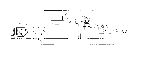
FIG.1 Is a block diagram comprising a circuit controlling the management and
collection of charges
through a capacitor (electrostatic storage device) referred to as a
"Deflection Converter".
FIG.2 Is an exemplified embodiment of the invention utilizing and converting
an alternating current
into a direct current for use as a deflection converter.
FIG.3 Is the preferred embodiment of the invention utilizing a management
system and controller
with an alternating current and configuration.
FIG.4 Is an embodiment of the invention demonstrating the preferred digital
embodiment with a
direct current power source and configuration.
FIG.5 Are illustrations of possible methods for integration as well as device
uses of the deflection
converter and its possible applications.
FIG.6 Is an illustration of possible utilization methods for implementation of
the deflection converter
technology.
25
CA 3010261 2018-06-29
=
14
Detailed description
Therefore, a heretofore unaddressed need exists in the industry to address the
aforementioned
deficiencies and inadequacies.
Figures and embodiments contained are to demonstrate possible variations and
to give a clearer
understanding of the theory and method herein, to allow one with ordinary
skill in the art to gain the
ability to re-create said method.
Embodiments of the present disclosure can also be viewed as providing systems
and methods for
managing and controlling the operational voltages and current from a current
source utilizing an
electrostatic storage devise and power converter in a novel way, operating
within a circuit with an
improved method and circuit design, this can be briefly described in
architecture one embodiment,
among others, can be implemented by;
Figure 1 is a block diagram of the device utilizing a management system 2 uses
a system for
managing energy, accumulation, storage, switch, power characteristic control,
and discharge
system, the device may be connected and controlled by any number of management
systems 2
and techniques and may include system controller 84 and or microcontroller.
The controller 84, may
be controlled by a computer code or script, embedded system, or artificial
intelligence, controlling
commands of the controller 84, connected to the circuit, may use a plurality
and multitude of
different switching devices 480, including interface(s), and current and
polarity control devices, and
may comprise different switching device 480 and or capacitor/ electrostatic
storage device 450
arrangements, which may also include a the transformer(s)56 which may be step
up and or step
down and or isolation transformer(s)56. The circuit may utilize power
available from the circuit or
operate on a separate isolated power source as shown. The input and output of
each electrostatic
storage device 450 may be connected to separate output switches 480 or a
single switch 480 and
or relay(s) (not shown) or not and or transistor(s) (not shown) or not, and
may include multiple relay
poles which could be any number of different types or styles for
electronically controlled switching
and or current control device 630, with all or some switches 480 controlled by
a CPU 78 or paired
with an existing CPU 78, in a non-limiting example of a master and slave
configuration. The CPU
78 may be controlled by a computer code or script, embedded system, or
artificial intelligence, that
tells the system controller 84, to send a signal to relay's (not shown) and or
transistors (not shown)
or switches 480 which may be connected to a power control device 630, which
may be connected
to a power converter 650 circuit and or system, charge booster converter and
or multiplier and or
buck converter and or switch mode power supply and or control circuit and or
converter 650, which
CA 3010261 2018-06-29
15
may or may not discharge through a load 500, and or another storage device to
create usable work.
In the preferred embodiment the current after the converter 650 is looped back
into the circuit to
create a feed back circuit and system which may be connected after the
converter 650 circuit and
which may be connected into the power supply side of the storage device 450
that is gaining a
charge and converted in this embodiment to a high voltage state to ensure
current draw, and may
be connected in either a positive polarity and or negative polarity
configuration, this may also
include additional pluralities of storage devices, power converters 650 and or
inverters or both
where a positive feedback into the positive power line before the capacitor
450 being charged is the
preferred embodiment.
Additionally some embodiments may utilize a management system 2 as a component
of the device
which may control various functions some of which may consist of one or more
of the following non-
limiting examples, the operation of all electronically operated components;
the charging and or
connecting and or disconnecting and combinational arrangements of an
electrostatic storage
device 450 and or storage device and or contact and or contact point(s); power
regulation means
46 for regulating power; a memory section, a search starting means 80 for
starting a search;
measurement data acquiring means 44 for acquiring magnetic field data and or
electric power data,
the magnetic field data being measured values of the energy sources and or
magnetic field and or
capacitor/ electrostatic storage device 450 data. The electric power data
representing information
associated with electric power that is outputted from the energy source 410 as
well as after the
electrostatic storage device 450 and or storage device and after the power
converter 650 and
required for operation and used by the management system 2 and or stored on
the electrostatic
storage device and or different circuit power lines and or sources. Functions
may also include
deriving means for deriving a relational equation that holds between the
magneti c field data and
electric power data to maintain target values including voltage and current
output and or capacitor
voltage potential state and feedback voltage state. Monitoring functions for
abnormal state
determining and may include means for determining whether or not the energy
source 410, a
collection device 450, or any energy switching 480, energy transforming and or
converting 650, or
managed circuits 2 are in an abnormal state. Searching functions 80 and a
search procedure,
selecting means for selecting, and in accordance with a result of
determination of the abnormal
state determining means, a procedure for managing abnormal energy sources,
magnetic fields,
accumulation devises 450, capacitor(s) and or storage device(s) 450, switching
devises 480,
transformers 56, management circuits 2, converter and or inverters 650.
CA 3010261 2018-06-29
16
In some embodiments, the management system 2 is needed to facilitate managing
the electric
current 410, then switching an electrostatic storage device 450 into the
current stream 410 and or
connecting power, then storing the collected charges in an electrostatic
storage device 450, while
simultaneously converting and regulating output power 650 and or feeding the
current back into the
power supply 410 to flow into the electrostatic storage device 450 then
switching collection devices
450 in circuit orientation and or disconnecting it from the circuit with a
switch 480 and or switches,
and then the storage device 450 may and or may not discharge collected
charges, which may be a
full or partial discharge. A system may require multiple switching of
accumulators and or electrical
storage devices 450; at a controllable rate, that can be replicated and
controlled to an extremely
high number of pluralities. To maximize energy from an energy source 410 and
or accumulators
and or electrical storage devices 450 which may be accomplished with current
42 and voltage 40
measuring devises, switches 480, accumulators and or electrical storage
devices and or including
capacitors 450, power converter(s) 650 and or AC converter(s) and or DC
converter(s) and or
inverter(s) and or transformer(s) 56 and or circuit controllers for instance a
non-limiting example of
PWM pulse width modulation, that may be in sequential and or parallel and or
series arrangements.
And in some embodiments a simplified management system 2 may be beneficial
utilizing some and
or different arrangement of listed or other functions, and additionally a
mechanical system in some
embodiment may be advantageous, for instance pairing with a commutator switch
(not shown), or
relays(not shown), utilizing the driving forced for controlling switching and
energy characteristics,
and in some embodiments utilizing no management system 2 instead using current
oscillators,
comparators, op amps, decade counter, motor, generator or natural means to
control the switching
480 force and or speed, this simplified management system 2 may be
advantageous for a
consistently regulated and or switching electrostatic storage device 450 and
or energy source 410.
Each circuit and module is an electrically connected system of components, and
may be managed
by the management system 2, which may include additional devises and systems
such as; a steady
electric current 410, circuit, a display 62, a direct current power
conditioner 50, current power
output interface 130, power converter 650, a thermometer 36, a thermometer
interface 116,
magnetic field sensor 34, magnetic field sensor interface 114, voltmeter 40,
voltmeter interface 120,
an ammeter 42, an ammeter interface 122, a measuring devise 44, a measuring
devise interface
140, an inverter 48, an inverter interface 128, a system controller 84, a
system controller interface
124, power control means 46, power system interface 126, a target value
setting capable device
54, a target value capable setting device interface 134, an input device 60, a
target value interface
136, an alternating current output interface 58, a transformer(s) 56, a switch
or switches 480, a
CA 3010261 2018-06-29
17
variable frequency drive 52, a variable frequency drive interface 132, a
central processing unit
"CPU" 78, a processor 74, estimating means 76, computing means 78, network
interface 138, load
500, search control means 80, relative relational expression equations 104,
abnormal
measurement memory 102, time series data memory 100, measurement data memory
98,
accuracy data memory 96, operating estimations data 94, target value memory
92, a rated value
database 90.
The control section can serve to control the overall control and operation of
various components of
the management system 2, circuits, modules, and the memory section can serve
to store
information. The control section may be configured to include a measurement
data acquiring
section (measurement data acquiring means 44), the amount of current/voltage
(current 42/voltage
40 acquiring means), a computing section (computing means 78), a target value
setting section
(target value setting means 54), a search control section (search starting
means 80), power system
section (power system controlling means 46), and in estimating section
(estimating means 76).
Further the memory section may be configured to include a target value memory
section 92, a
memory section 98, and a relative relational expression equation section 104,
a rated value
database 90.
The memory section serves to store, as measurement data 98, measurement data
obtained from
each measuring instrument while the management system 2 is operating.
Specifically, the
measurement data 98 may contain the following measured values measured at the;
measure point
of time, operating current value(s), operating voltage value (s), amount,
magnetic field strengths,
and temperature. The measure point in time is data representing year, month,
day, hour, minute,
and second. Further the operating current value in operating voltage value
refer to values of an
electric current and voltage is measured at a point, respectively.
Further, temperature may be measured by the thermometer 36; magnetic fields
are measured by a
magnetic field sensor 34. The rated value database 90 is provided with a
memory section and a
target value memory section. The memory section serves to store relative
relational expression
equations 104, for maintaining operating current values and operating voltage
values. The target
value memory section serves to store target values 92 of the operational
estimations 94, and
accuracy of relative relational expression equations 96, that determine power
usage and magnetic
field strength relations, to ensure optimal system performance and efficiency,
that can be
interpreted for command allocation.
CA 3010261 2018-06-29
18
The measurement data acquiring section, may serve to acquire measuring values
from each
measurement instrument. Specifically, the measurement data acquiring section
may acquire
measurement data of (electrical power data, temperature, magnetic field data),
which is time-series
data, containing the electric current value(s), the voltage value (s), the
temperature, the magnetic
fields, from the measuring instruments of the ammeter 42 and voltmeter 40, the
magnetic sensor
34, thermometer 36, and from the electrostatic storage device 450 and sends
the measurement
data to the search control section 80 of the database 90.
The search control means 80, may search for relative relational expression
equations 104, to
interpret historical relations to measurement data values 98, and interpret
proportional relationships
between stored measurement values 98, operational characteristics, and
predetermined target
value ranges 92, including output characteristics, discharge relational
information including
combinational arrangement output power data, cluster and module combination
data, looping circuit
and or feedback value, and duty cycle optimization equations.
The search control means 80, may compute measurement characteristics if
measurements have
been measured and stored even once and can compare characteristics with the
target value setting
section 54/134, which may also incorporate a learning effect, or artificial
intelligence, interpretations
can be interpreted by the central processing unit CPU 78, which can send
instructions to the
system controller 84, which can then send command signals to active switching
480 and control
systems, and components, to control predetermined, or instructed operational
tar get values 92 and
functions.
The measurement data acquiring section, may also serve to determine faults, by
acquiring and
comparing measured values from the measurement data memory 98 storage section,
and by
interpreting abnormal operating system measurements 102. Abnormal measurements
102, may be
stored in the memory storage section, and additionally may be sent to the
display 62, to indicate to
users of the management system 2, abnormal measurements 102, or may be sent to
the control
section and the target value memory section, and may perform tasks such as
bypassing abnormally
operating circuits, modules, systems, or component's, and or by
compartmentalizing systems
containing faults and maintaining predetermined target operating conditions,
output power
characteristics including feedback and or looped power circuits and or lines,
and may control
simulated and or virtual loads and or current limiting/ controlling devices
and or circuits and or
functions.
CA 3010261 2018-06-29
19
It should be noted that measurements may be computed by performing
measurements by
measuring each instrument once, or more than once, at a time of introduction
of the management
system 2 or may be computed as a search performed manually by the user's
operating the
management system 2, or maybe performed automatically, e.g., regularly. In
particular
measurements may be performed at predetermined intervals, or from time to
time. The exacting
control of the electromagnetic, electrostatic and electrochemical fields under
the devices
management is a main primary concern of the disclosed invention, switching
consumption is of
concern in order to not reach an inefficient level, though a certain trade-off
of output energy and
energy consumption occurs.
Included as possible embodiments a multitude of current and or voltage sensing
and triggering
techniques may be used and are referenced herein as possible alternate
embodiments and are
explained in the section "Initiating and Control Methods". As well in this
embodiment a switch is
used though in other embodiments a number of switching devices and methods may
be used and
are referenced herein as possible alternate embodiments and are explained in
the section
"Switching Methods and Devices", and may incorporate a management system or
process and
are referenced herein as possible alternate embodiments and are explained and
referenced in the
"Management Systems and Processes" section. A circuit may benefit greatly by
designing
architecture to change a circuit's resistance and or current during operation
and are referenced
herein as possible alternate embodiments and are explained and may be
accomplished with
.. reference to the section "Resistance and Current Control". This resistance
may be used to
control the current and or voltage to ensure the desired output power at
different stages of the
capacitor operation, and or during operation of a varying potential and or
current power supply or
source, referenced herein are possible alternate embodiments and are explained
and may be
accomplished with reference to the section "Current Source and Power Supply".
Additionally, the
operation of the device and electrostatic storage device/ capacitor 450 system
and allow for a
number of possible output current states and ranges including connection
points and feedback
referenced herein are possible alternate embodiments and are explained and may
be
accomplished with reference to the section "Output Characteristics". Though a
management
system 2 is described and referenced possible alternate embodiments are
additionally referenced
.. herein and are explained and may be accomplished with reference to the
section "Integrated
Circuits". Though a capacitor 450 for charging is referenced possible
alternate embodiments are
additionally referenced herein and are explained and may be accomplished with
reference to the
section "Storage devices". Though a generic load 500 is referenced possible
alternate
CA 3010261 2018-06-29
20
embodiments are additionally referenced herein and are explained and may be
accomplished with
reference to the section "Implementations" as well as the section
"Applications".
Figure 2 illustrates an exemplified embodiment comprising a circuit
controlling the management of
charges and or potentials for charging a capacitor (electrostatic storage
device) 450 herein after
referred to as a "Deflection Converter" 700. The design of the circuit allows
a power sources current
to flow, in this case an AC power source 420 into and out of the deflection
converter by means of a
switch and or switches in this case a double pole double throw relay 490, it
should be noted the
deflection converter 700 in some embodiments may be a stand-alone charger and
in other
embodiments may be directly built into a the device(s) which may able to be
used with a multitude
of power source(s) which may connect or be connected with via swi tch(s), and
or made to allow
contact for an electrical connection and or may connect electrically through a
wireless and or
transmitted operation. The relay 490, which could be any number of different
switches and or
transistors 350 and or solid state and or mechanical switches controlling the
operation of the
capacitor(s) 450 leads in the circuit, which could be a smaller or larger
capacitance depending on
an individual application and duty cycle. The relay 490 allows the power
supply's energy to enter
into the relay 490 and exit into a circuit, then into the capacitor 450
storing charge in a reverse
polarity and or orientation transferring energy from the circuit to the
capacitor at 100% efficiency
less operating losses. After exiting the capacitor 450 the power flows into a
power converter 650
where the voltage is increased above the supply voltage state and reconnected
to the circuit before
the capacitor 450 to cause a continuous draw of current, and due to the energy
conversion of the
converter 650 the current flow increases exponentially causing decreased
charging time and
increased efficiency because the output current is converted and fed back into
the capacitor 450 to
further charge the capacitor creating a current loop and or feedback system.
In some embodiments multiple power sources 420, and or loads 500 may be
utilized which may not
be required and or. may be replaced with virtual/ simulated loads non-limiting
examples may include
electronic loads, current limiting drive circuit(s), clamp circuits, current/
inductive chokes, current
sink(s), dummy load(s), load circuit and or controller, resistor based load,
capacitor 450 in circuit
angle can be redirected to a different current source 410 and or looped with
converted electrical
current feedback connected to the high side of a positive polarity charging
circuit and or to the
lower side of a negative polarity charging circuit and or combinational or
varying connection that
may utilize pluralities of charging circuit(s) and capacitor (s)450
arrangement to exploit and utilize
this beneficial feedback loop during charging operation, further change in
circuit orientation may be
CA 3010261 2018-06-29
21
utilized in different embodiment to effectively charge capacitor(s) 450 at
different potential states,
and or steps, additionally all owing operation in a plurality and or series
design. The different
quantities of capacitance of the capacitor(s) 450 effects duty cycle and
operation, in that the
charging time is extended or decreased, as time is needed for charges to
collect in the capacitor
450 which is additionally affected by the rate of current flow from the power
source 420, where a
high rate of flow may cause in some embodiments an almost instantaneous charge
rate on a
capacitor 450 and may require current limiting and or smoothing with non-
limiting examples of
passive and or active snubbers and or clamps which may be positive polarity
negative polarity and
or unbiased, PWM converter that may be used for clamping, clamp branch diode
and capacitor,
coupling inductor, current limiting circuit, current mirror, and or electronic
load controller. Where
time is of primary concern series configurations of capacitors 450 at higher
voltages from the power
source 420 and current flow may be preferred, this embodiment would allow use
in a parallel type
discharge arrangement similar to a charge pump configuration. In additional
embodiments where
flowing current is more reduced or limited parallel arrangements of charging
capacitors 450 with
extended time periods of charging may be preferred, in further embodiments a
high frequency
switch(ing), between a state and or states, may also provide a stable
beneficial output.
Additionally, another switch such as a non-limiting example of an IGBT
transistor (not shown) may
be added to give a direct short connection between the switching capacitor 450
and power source
410 and or substitute mechanical switches, this may be used to cause the
voltage to continue
causing a force charging the capacitor 450 though not preferred. In some
embodiments the power
source 410 may be supplied directly from a DC current, in this embodiment it
may be possible to
eliminate an input power converter/ inverter and or rectifying circuitry and
or systems/ devices (not
shown), additionally improving the efficiency of the deflection converter. In
many embodiments the
operation of charging the capacitor 450 to a maximum state may be beneficial
as current
conversion may cause expedited charging rates, wherein an operating range may
be more
preferred to allow continuous operation and maintain an effective and
efficient duty cycle of a power
converter 650 and or boost converter optimizing operating characteristics.
Operation can be across the full range of voltages, the capacitor 450 may be
operated over a range
or power band that utilizes high voltages and reduces the charging time,
effectively increasing the
amount of energy benefit over a given period of time. This is due to the
capacitor 450 being
charged at a low initial resistance, then being introduced at the power
sources 420 voltage so the
operational voltage and resistance symmetry operates automatically in the most
efficient manner
possible this is do to the exact matching and coupling of the instantaneous
change between the
CA 3010261 2018-06-29
22
power source current 420, capacitor 450 energy state and resistance. The due
to the voltage drop
across the capacitor 450 the power converter 650 must increase it switching
frequency causing a
draw of current that continues to increase as the difference in voltage state
grows between the
capacitor 450 output feed in the converter 650 and the converters 650 output
voltage level, that is
then looped and fed back into the circuit before the capacitor 450 continuing
the cycle.
In some embodiments the operation of charging the capacitor 450 may benefit by
the use
resistance for as one non-limiting example current limiting, additionally
resistance may be used to
divert and or clamp and or control only a potion of the fl owing current 420
which in embodiments
with a high voltage and current flow may be beneficial and in certain
embodiments necessary, a
few non-limiting examples resistances may include a varistor or voltage
dependant resistor,
potentiometer and or controlled by a servo motor, or arrangement of different
resistors 340 and
resistances controlled by switches and or transistors 350.
In the preferred embodiment a supervisory IC 600 is used to sense the voltage
on the low side and
or output of the capacitor 450 while charging, which is used to initiate a low
current state and or
send a signal to the NE555 timer 530 which is configured in a monostable
configuration, the NE555
timer 530 sends a signal to the LM4017 Decade Counter 560 which controls a
transistor 350
controlling the relay 490, though is some embodiments the relay 490 may not be
used as the
transistor 350 and or transistors could control the power supply current 420
directly, as well as the
LM4017 560 could be replaced with for instance a flip-flop and or not used as
switching could be
directly driven with a controller and or digital logic and or logic levels,
and or with the use of
comparators and or op amps. The supervisory IC 600 sends a signal to the NE555
530 timer when
the voltage output from the capacitor 450 reaches the desired voltage,
determined by the desired
charge that is stored on the capacitor 450 after charging, measurable by the
output voltage due to
the voltage drop caused by the capacitor 450. The supervisory IC 600 may also
be replaced with
over/ under voltage reset IC's and may also utilize Zener diodes and resistor
340 combinations in
conjunction with voltage sensing devices with for instance comparators and or
op-amps and or
reflective feedback as well in some embodiments an analog to digital converter
may be used and
allow digital sensing and or control. The output current may be converted 650
to a desired voltage
and or current limited with the use of a simulated load 500 and or current
control and or inverter 48
such as a boost converter and or inducing a controlled current in a
transformer (not shown), and
may additionally utilize a voltage regulator 330 or not, that may utilize
capacitors 360 thought the
voltage regulator may not be required in many embodiments because the voltage
of the circuit may
be of a higher potential then the desired charge point of the capacitor 450 as
well as the output
CA 3010261 2018-06-29
23
current may be routed through a power converter for stabilization and may be
fed back into the
circuit to continue charging the capacitor at a higher voltage state to ensure
current draw and a
constant and or increasing current which is preferred.
Additionally some embodiments may utilize pluralities of deflection converters
and or capacitors
450 and or electrostatic storage devises 450, either in series and or in
parallel or a combinational
arrangement of both, and different sizes of capacitors 450 may be utilized to
increase the time rate
of charge conversion and or extraction in the circuit for instance a series of
capacitors 450, wherein
each capacitor 450 operates at a lower overall combined capacitance increasing
voltage tolerance
and providing equal current through each capacitor 450 and the circuit to
increase charging speed
.. and or frequency.
Additionally consecutive capacitors 450 may not necessarily need in series
arrangements instead
the capacitor(s) 450 operation could be timed to operate at different
switching points in time, the
ideal operation of this configuration could have a single or plurality of
capacitors 450 being charged
while reducing circuit voltage while simultaneously a single or plurality of
additional switching
capacitors 450 are not connected or charging and having no effect on circuit
voltage, this operation
could operate if the output was compensated for with a non-limiting example of
a converter 650 for
instance a boost converter and or inverter 48, wherein current rate would
increase through the
capacitor 450 providing for an increased capacitor 450 charge rate.
The operation of the circuit in the preferred embodiment is designed to allow
automation of the
deflection converter within a predetermined operating range; this may be
accomplished by utilizing
a supervisory IC's 600 or reset/ set reset IC's, though a comparator and or op
amp may be used in
some embodiments that may utilize feedback and hysteresis and or a Schmitt
trigger. This
configuration allows the output current that is continually decreasing voltage
after the capacitor 450
to be measured and compared against a reference voltage 290. The reference
voltage is a
predetermined and or controlled voltage that is used to provide a point in
which the switching of a
capacitors 450 out of the circuit is triggered. This reference point could be
determined by a number
of factors including capacitor 450 voltage rating and or capacity and or
circuit voltage requirement
and or power source 420 cut out and or operation limit voltage and or
oscillation frequency
requirement and or circuit tolerance to fluctuations and sensitivity to
fluctuation, ripple or noise just
.. to name a few non-limiting examples.
This operational method is advantageous because the output current is not the
primary determent
for activating the operation of switching the capacitor 450, instead the
circuit voltage is the
CA 3010261 2018-06-29
24
determining factor in the operation cycle, and as such this circuit design can
be utilized in many
different devices from high current consuming devices to devices that consume
only a small
amount of current without negatively affecting the device operation, though in
some embodiments
of predictable or set current a current measurement or predetermined volume
may be used to
trigger switching operation.
The operation of an auto mated circuit provides for a controllable system to
effectively utilize the
positive benefit and maximum efficiency charging a capacitor 450 in a straight
forward
uninterrupted operation. The input power source 410 is connected to a
supervisory IC 600, which
may additionally be a comparator with a Zener diode of appropriate value and
or a voltage regulator
or voltage reference, to tie down the voltage reference detected by the
comparator (not show) to a
non-floating value; in some embodiments a floating voltage for reference may
be preferred, in some
embodiments the reference voltage would be al lowed to float as the dc power
source 430 voltage
fluctuated this could allow a moving voltage range while charging the
capacitor 450 while for
instance a battery is discharging through its operable power range or band. In
additional
embodiments a comparator (not shown) in some embodiments is in an inverting
configuration so
that when the voltage is being compared against the reference voltage drops
below the reference
voltage 290, the comparator sends out a signal and or stops conducting
current, in the preferred
embodiment this action is accomplished with a supervisory IC 600, to the NE555
timer 530. In
some embodiments instead of an inverting configuration operation it may be
beneficial to use a
non-inverting configuration and operation, or additionally some embodiments
may benefit by
utilizing multiple and or pluralities of comparators (not shown) which for in
the case of utilizing two
comparators (not shown) could operate within a window of operation, wherein
one comparator is in
an inverted configuration and the other comparator ( not shown) is in a non-
inverting configuration
and the capacitor 450 charging operates within a voltage window or range,
which could be greatly
beneficial if multiple circuits and or loads 500 utilized a plurality of
comparator windows to operate
in each of their desired voltage ranges, while the capacitor 450 charging is
operating and
fluctuating which causes an increase and decrease in circuit voltage
potentials, effectively utilizing
an optimal power window throughout the capacitor 450 charging cycle.
The voltages sensed by the supervisory IC 600 can be controlled using
resistors 340 as well as
potentiometers 380, and or feedback, which can be greatly beneficial in
controlling operating
characteristics and voltage ranges to very accurate measurements, as well as
utilizing hysteresis to
create a buffer or filter gap between the two thres holds of an op-amp (not
shown) sensed voltages
290, this introduction of hysteresis can be greatly beneficial as it can
reduce or eliminate false
CA 3010261 2018-06-29
25
triggering or jitters that may become apparent in the operation of the circuit
and or op-amp and or
relay(s) 490, which can become quite predominant with lower currents and slow
voltage transitions.
This false triggering can cause the operati on of the circuit to cease and or
be disturbed and as such
methods to overcome this operational challenge are paramount, different
methods to overcome
jitters and false triggering include hysteresis, reducing switching capacitor
450 capacitance to
cause an increase speed of voltage transition , operating the control circuit
on a different power
supply 410 to remove any noise or interference to "clean up" the power source
420. Measurements
can be used to create high frequency switching, as well as a full range of
switching speeds and
voltage levels both for output and or to capacitor 450, which in some
embodiments may utilize a
prolonged period between switching.
The output current controlled by the supervisory IC 600 is sent and
electrically connected to a
NE555 timer 530, the NE555 timer 530 is used to create a uniform square wave
with both rising
and falling edges, which in some embodiments may utilize an operational
amplifier for the voltage
comparison and may additionally use a number of different methods to
facilitate the a trigger point
to initiate or control the act of switching the capacitor(s) 450.
The NE555 timer 530 configured as monostable or "one shot" configuration
accepts the signal and
or current state change from the supervisory IC 600 and sends out a square
wave signal pulse in
this embodiment to a LM 4017 decade counter 560, the decade counter 560 is
used to control a
transistor 350 through a resistor 340 that controls a relay 490 which may
contain a "fly back diode"
300 to suppress voltage spikes during switching though transistors are
preferred for instance
IGBT's, to facilitate the action of switching a capacitor 450 into an
operating circuit. Though a
number of devices such as flip flops, set reset circuits, latching circuits,
and or counting or stepping
circuits may be used, in this embodiment the LM 4017 decade counter 560 is
used to create an on
state and off state step, as the voltage drops below the reference voltage
then hold the relay 490 in
an on or off position, in this embodiment a double pole double throw relay
490, is held in either a
normally open or normally closed position which changes the circuit
orientation and connects/
inserts the capacitor 450 into the current stream though in the prefer red
embodiment solid state
electronic switches are preferred.
The output current is used as the voltage being monitored 290 as it is the
current that's voltage is
affected by the capacitor 450 charging operation, the control current is
accomplished by electrically
connecting this point in the circuit with the Vin (Voltage IN) of the
supervisory IC's 600 which after
the switch occurs creates a reducing voltage in the output power line which is
additionally sent to
the supervisory IC 600 which senses the lowering voltage and then changes its
output state, it
CA 3010261 2018-06-29
26
should be noted the LM4017 dec ade counter 560 maintains its output pin state
even after the signal
from the NE555 530 has ended, the duration of which may be controlled by
varying the control
resistor 340 and capacitor 360. In some embodiments the LM 4017 decade counter
560 may not be
necessary as the signal from the NE555 timer 530 or the comparator or an
operational amplifier
(not shown) or additional voltage sensing devices.
The preferred configuration of the NE555 timer 530 in the circuit is in a mono-
stable or "one- shot"
configuration though in different embodiments it is possible to utilize
different configurations
including astable, bistable, multivibrator or triggered and could be used as a
dir ect drive to the
switching means of the capacitor 450, which may also include controllers,
microcontrollers and
other directly driven outputs for control. The LM 4017 decade counter 560 in
this embodiment is
configured to operate as a 1-2 counter, specifically the decade counter 560
operates to count
between the output pins 0 pin and the 1 pin with the 2 pin being the res et
pin, this is to allow the
relay 490 to alternate between being in an off position, or on position based
on a single signal sent
out from the supervisory IC 600 and or comparator (not shown) each time the
voltage crosses
below the V Ref or voltage reference, this crossover point would be the point
in which the capacitor
450 is charged to the desired voltage and or the charging of the capacitor 450
commencement
point when the current is channeled through the capacitor 450.
This on off operation of the transistor 350 and relay 490 is accomplished by
electrically connecting
to only one of the LM 4017 decade counter 560 output pins, though in some
embodiments different
output pin arrangements could be used in conjunction with a relay 490, a
switch or switches to
facilitate the operation of changing the in circuit orientation of the
capacitor 450, and or connecting
the capacitor 450 to different circuits and or connecting the deflection
converter 700 to different
capacitors and or the same capacitors 450 at different points in time.
In this embodiment the DPDT relay 490 is connected to the capacitor 450 so
that, for simplicity,
when in the first normally closed position the current is allowed to travel
into the relay 490 and into
the capacitor 450, then back into the relay 490 and then into a power
converter 650 and or inverter
48 and or directly connected into the circuit supplying power to the capacitor
450, then the voltage
may be monitored by under/ over voltage supervisory IC's 610, that controls
the trigger point of the
deflection converter to change the relays 490 state.
When the DP DT relay 490 is activated by the transistor 350 allowing current
to activate its coil and
move into the second normally closed position which for simplicity will be
referred to as the
normally open position, the power supply current 420 then travels into and
then back out of the
CA 3010261 2018-06-29
27
relay 490 unobstructed in this embodiment, while the deflection converter
remains in an off sate
and or standby state.
It should be noted that in this embodiment the capacitor 450 is located
upstream in positive polarity
though in other embodiments the capacitor(s) 450 in circuit locations may be
made to operate in
negative polarity and or altered without departing from the benefit and
operation of the disclosed
invention.
Additionally, though in this embodiment the current being monitored and sent
to the supervisory IC
600 is located after the capacitor 450, it may be beneficial to sense the
voltage in any number of
positions within the circuit to optimize the device for specific applications
and for different operating
techniques and procedures, which may be made visual through the use of
optional LED's 370 and
or output display. Additionally, filtering of noise may be of consequential
importance in
embodiments where a single power source 420 or shared power source is used in
conjunction with
a sensor or sensors controlling the switching action of capacitor(s) 450, and
filtering may be
accomplished with non-limiting examples of low pass active filter, high pass
active filter, multiple
sample comparison reference, low pass passive filer, high pass passive filter,
Schmitt trigger,
clamps, snubbers as well as additional stabilizer capacitors may be used to
ensure during the
transition periods of the relay 490 and or switches. Additionally, some
embodiments may benefit
from utilizing latching relays 490 and or switches to facilitate switching
operations of the
capacitor(s) 450.
Additionally, in some embodiments it may be possible and beneficial to send a
single signal from
any number of devices to facilitate the operation of switching the capacitor
450, wherein digital
processing and or logic levels could be used to operate the switching action
and charging
capacitor(s) 450 operation. This may be the case in for instance mobile
devices where current
levels are continuously monitored and implementation would only require a few
additional
components as in the capacitor 45 and switches 480, as all other operations
are currently being
accomplished by active systems on the device.
The benefit and operation of the deflection converter can be increased further
by utilizing additional
sequential capacitors 450, the operation of which presents its own challenges,
the i deal
embodiment for multiple sequential capacitors (not shown) that may be any
number of pluralities or
series configurations, and by operati ng for instance a second capacitor (not
shown) within an
operating range and specifically by utilizing a lower, the same, or a
different capacitance for the
second switching capacitor (not shown) that operates at a higher switching
frequency, which in
CA 3010261 2018-06-29
28
some embodiments may operate in this manner as multiple stages or nodes, and
or may
additionally be operated in a parallel fashion at the same voltage state, or
at a different voltage
state(s), stage(s), or step(s).
The operational circuit current can operate in a number of different
operations, the current can be
regulated, both on the input of the circ uit to stabilize the voltage
monitoring and control portion of
the circuit, as well as the output current may be additionally voltage
regulated, or not, depending on
specific applications requirements and sensitivity, and or routed to power
circuits based on the
current state of voltage, for each circuit, maximizing the power and work
product at that point in
time. A circuit may benefit greatly by designing architecture to change a
circuit's resistance during
operation referenced as possible embodiments herein which may be accomplished
with reference
to the section "Resistance and Current Control". This resistance may be used
to control the
current and or voltage to ensure the desired output power and or feedback at
different stages of the
capacitor 450 charging and or during operation of a varying potential and or
current power supply
420 and or source.
.. Included as possible embodiments a multitude of current and or voltage
sensing and triggering
techniques may be used and are referenced herein as possible alternate
embodiments and are
explained in the section "Initiating and Control Methods". As well in this
embodiment a switch is
used though in other embodiments a number of switching devices and methods may
be used and
are referenced herein as possible alternate embodiments and are explained in
the section
"Switching Methods and Devices", and may incorporate a management system or
process and
are referenced herein as possible alternate embodiments and are explained and
referenced in the
"Management Systems and Processes" section. A circuit may benefit greatly by
designing
architecture to change a circuit's resistance during operation and are
referenced herein as possible
alternate embodiments and are explained and may be accomplished with reference
to the section
"Resistance and Current Control". This resistance may be used to control the
current and or
voltage to ensure the desired output power at different stages of the
capacitor operation, and or
during operation of a varying potential and or current power supply or source,
referenced herein are
possible alternate embodiments and are explained and may be accomplished with
reference to the
section "Current Source and Power Supply". Additionally, the operation of the
device and
electrostatic storage device/ capacitor 450 system and allow for a number of
possible output
current state and ranges referenced herein are possible alternate embodiments
and are explained
and may be accomplished with reference to the section "Output
Characteristics". Though a
management system 2 is described and referenced possible alternate embodiments
are
CA 3010261 2018-06-29
29
additionally referenced herein and are explained and may be accomplished with
reference to the
section "Integrated Circuits". Though a capacitor 450 for charging is
referenced possible
alternate embodiments are additionally referenced herein and are explained and
may be
accomplished with reference to the section "Storage devices". Though a generic
load 500 is
referenced possible alternate embodiments are additionally referenced herein
and are explained
and may be accomplished with reference to the section "Implementations" as
well as the section
"Applications".
Figure 3 is the preferred embodiment of the invention utilizing and converting
an alternating current
420 into a direct current for use as a deflection converter to charge an
electrostatic storage device
which then feeds back into the positive power line to loop the current from
the output of the storage
device which is converted to a voltage slightly above the voltage state of the
power line supplying
the capacitor to maintain a draw of current, and though in this em bodiment
the alternating current
420 is converted through a transformer 640 and then into a bridge rectifier
310 and entirely to direct
current for charging a capacitor 450 and then looped as its operational
circuitry, in additional
embodiments the alternating current 420 does not need to be converted into
direct current instead
the capacitor 450 utilizing the disclosed method could be implemented to offer
the same benefit as
in DC circuits if the capacitors 450 operation was timed to switch orientation
within an alternating
current 420 before each alternation was to take place, or as a product of each
alternation.
For example in an embodiment with an AC source 420 powering an AC induction
motor (not
shown) operating at a frequency of 50 hertz single phase, what this means is
the current is a single
alternating current and it alternates at 50 alternations a second. With the
disclosed method, if each
alternation is considered to be a direct current source, between each
alternation, then by utilizing a
switch for the capacitor 450 it is possible to invert the charging and
discharging of the capacitor 450
within each alternation of the main supply current 410 which because of the
requirement of higher
frequency operation a transistor for the switching operation is preferred.
Explaining this in operation, as the alternating current 420 is flowing in the
positive sine of the
alternation the capacitor 450, which is first charging the capacitor 450 and
supplying a decreasing
current and voltage to an electrical grid, then when the cur rent begins to
alternate the direction of
the capacitor 450 is reoriented into the current stream to continue charging,
this re-introduction can
occur both within a single alternation, or may be accomplished within the next
alternation, or
completed cycle, wherein a single alternation can comprise the entire
operation of charging and
CA 3010261 2018-06-29
30
discharging/ disconnecting the capacitor 450. Additionally, the charging may
be accomplished over
an entire cycle of the alternating current power source 420, where the
capacitor 450 is charged in
one half of the cycle and or both half's of the alternation and or after the
alternation and or before,
or additionally charged in both half's of the cycle and or the next operating
cycle or multiple
alternations/ cycles.
In this embodiment the alternating current 420 is fed into a transformer 640
which depending on
the input voltage and current may be either a step up, or step down
transformer 640, in some
embodiments no transformer is required where a power converter(not shown) may
be implemented
for instance a non-limiting example of a switch-mode power supply(not shown)
and or PWM current
control is implemented, the transformer 640 is then connected to a bridge
rectifier 310 which in this
example is a full wave rectification but may also comprise a half wave bridge
rectifier (not shown)
and or multiphase rectification, or again may not be necessary and or
substituted for more efficient
devices for instance rectification controlled by mosfet and or other
transistors such as IGBT's,
which have been shown to operate at high efficiency's. The current is then
routed through a voltage
regulator 330 which is optional in this example an voltage regulator IC is
used which could regulate
the voltage to a range of desirable levels, which could also include a
controlled regulator to actively
change the desired operating voltage fed to the circuit, and which could
include a number of
voltage regulators 330 and or plurality for use with multiple circuits and or
capacitors 450 and or
deflection converters, with additional capacitors 450, in this embodiment used
as decoupling and or
filtering capacitors 360 are used. The current located after the capacitor(s)
450 then supplies a
main power line used as the sensing voltage 290 and or current that is fed
back into the high side
of the capacitor in the power line, in this example a separate voltage
regulator (not shown) is not
used, though in an exempl ary embodiment a separate power source (not shown)
and or voltage
regulator (not shown) and or resistor(s) or variable resistor 340 may be used
to supply sensitive
operating circuitry with a smooth stable power source 410, additionally in the
preferred embodiment
the output may be controlled by a power converter and or power inverter 48 and
or power control,
converter, inverter, booster, reducer! buck, and or electronic either digital
or analog controller to
provide a desired output current and voltage that may be looped back into the
power lines and may
be connected in either a positive and or negative polarity charging design,
which may be a direct
current, the preferred alternating current, pulse width modulated and or
variable current which may
additionally supply a simulated and or virtual load, and may include current
limiting chokes and or
control circuitry such as snubbers, PWM, resistors and or resistance and or
switching current
control.
CA 3010261 2018-06-29
31
In this embodiment a management system 2 and controller is used to carry out
the functions and
operation of the deflection converter which may be substituted with a number
of control systems, in
this embodiment the current sensing operation is converted into a digital
format to allow ease of
operation and accuracy controls that may use program codes and or algorithms.
The controller 2
controls a transistor 350 that controls a relay 490 which may incorporate a
"fly back diode" 300,
which may compose any number of switches such as transistors. The relay 490
controls the
operation of switching the capacitor 450 and it's in circuit orientation and
connection to current
supplying the feedback loop and or simulated load(s). In this embodiment
voltage sensing,
measurement, and triggering the switching of capacitor(s) 450 is accomplished
with analog to
digital connection and conversion, though in some embodiments may be
accomplished by using a
current and voltage limiting connection that may compose a resistor and or
resistance divisible into
a digital count for conversion of voltage state and current, and or may
include an analog to digital
and or digital to analog converter and or measuring devices such as non-
limiting examples of
ammeter(s), voltmeter(s), pyrehelometer(s). The capacitor 450 outputs current
into a relay 490 and
or a system of or a transistor(s) 350 that control the current and voltage
into a power converter and
or control circuit that may power a load(s) 500, where voltage is increase and
feedback into a
positive polarity power line is preferred, though in some embodiments a
negative polarity power/
ground line may be preferred for design and operational purposes.
This configuration of transistors 350 in additional embodiments could be used
to allows the current
to travel into desired resistance paths based on a point in time, and or the
voltage of the capacitor
450 and or output current, the reason for this is the deflection converters
benefit is realized over the
range of charging the capacitor 450.
This decreased current and its effect on decreasing circuit power may be of
great usefulness in
certain embodiments, specifically for power savings, though for a number of
embodiments the
benefit of the deflection converter operation would more greatly be realizing
voltage swings, so in
these embodiments the amount of circuit current may be controlled by a power
converter and or
inverter or power controlling means, to control the output current and voltage
feedback. This in
some embodiments may operate by controlling switches such as transistors and
as the output
voltage is reduced and or reducing, activate different transistors and or
switches and or with
inductors and or with diodes and or with capacitors, to offer an increased
frequency to the output
current to increase the declining voltage and allowing circuit voltage and cur
rent to remain
consistent, which may be across any plurality of switching systems and or an
operational range
controlling a the device(s) and or virtual loads and or feedback circuits.
Additionally, the
CA 3010261 2018-06-29
32
requirements and or current frequency and or capacitor 450 voltage state may
be controlled to
precisely meet the operational requirements and deter mined voltage range of a
specific
application(s) and or systems.
In certain embodiments a simplified system and operation can be greatly
beneficial for ease of use,
cost and operation wherein the specific application has consistent energy
consumption, additionally
this operation and direct drive configuration could also be used in some
embodiments to directly
drive a latching switching device, for instance a latching relay 490, and or a
partial rotation of a
commutator switching apparatus wherein brushes or contacts make an electrical
connection to an
alternate an electrical configuration and or circuit configuration(s) for
operating the capacitor (s) 450
.. charging and or switching operation and or feedback.
Additionally, a control source and or controller may drive a latching
electronic device for instance an
IGBT transistor that if the gate on the IGBT is not pulled down with a pull
down resistor then after
the gate is "charged" would remain in an on state until a pull down or
discharge of the gate occurs,
and in this example many different methods could be used to operate this
device in a timed,
consistent or periodic manner for instance a separate pull down transistor or
high value resistor and
or a current state change sent from the controller 2.
Included as possible embodiments a multitude of current and or voltage sensing
and triggering
techniques may be used and are referenced herein as possible alternate
embodiments and are
explained in the section "Initiating and Control Methods". As well in this
embodiment a switch is
used though in other embodiments a number of switching devices and methods may
be used and
are referenced herein as possible alternate embodiments and are explained in
the section
"Switching Methods and Devices", and may incorporate a management system or
process and
are referenced herein as possible alternate embodiments and are explained and
referenced in the
"Management Systems and Processes" section. A circuit may benefit greatly by
designing
architecture to change a circuit's resistance and or current during operation
and are referenced
herein as possible alternate embodiments and are explained and may be
accomplished with
reference to the section "Resistance and Current Control". This resistance may
be used to
control the current and or voltage to ensure the desired output power at
different stages of the
capacitor operation, and or during operation of a varying potential and or
current power supply or
source, referenced herein are possible alternate embodiments and are explained
and may be
accomplished with reference to the section "Current Source and Power Supply".
Additionally, the
operation of the device and electrostatic storage device/ capacitor 450 system
and allow for a
number of possible output current states and ranges including connection
points and feedback
CA 3010261 2018-06-29
33
referenced herein are possible alternate embodiments and are explained and may
be
accomplished with reference to the section "Output Characteristics". Though a
management
system 2 is described and referenced possible alternate embodiments are
additionally referenced
herein and are explained and may be accomplished with reference to the section
"Integrated
.. Circuits". Though a capacitor 450 for charging is referenced possible
alternate embodiments are
additionally referenced herein and are explained and may be accomplished with
reference to the
section "Storage devices". Though a generic load 500 is referenced possible
alternate
embodiments are additionally referenced herein and are explained and may be
accomplished with
reference to the section "Implementations" as well as the section
"Applications".
Figure 4 is an exemplified embodiment of the invention utilizing a simplified
direct current power
source 430 and configuration, for use as a deflection converter and
demonstrates the preferred
digital embodiment of the device utilizing a management system 2, direct
current power source 430
and configuration, for use as a deflection converter. This simplified
configuration utilizes a DC
power source 430, the current may then be routed through an optional voltage
regulator (not
shown), the current then supplies a main power line which in some embodiments
may be used for
sensing the voltage 290 and or current supplied to the power converter. In
this embodiment a
management system 2 utilizing a controller 84 is used to control the operation
of the deflection
converter with transistor(s) 350 as the switching mechanisms for operation.
The transistors 350
control the operation of the charging capacitor(s) 450 and it's in circuit
orientation supplying current
to a power converter, which includes a feedback loop, and or to ground 440 and
or a lower
potential. In this example voltage sensing is accomplished with a pull up
sensing resistor 340 from
the electric feed after the charging capacitor 450 and before the power
converter 650. The
management system 2 configuration utilizes a DC power source 430 though in
alternate
embodiments may utilize an alternating current power source or sources (not
shown) or varying
source such as a electrostatic storage device (not shown). The current may be
routed through an
optional voltage regulator (not shown) or there may exist multiple separate
power sources or
"lines", and in additional embodiments a variety of switching devices may be
used to control power
sources 430 and or lines, and or including feedback. The current then supplies
a main power line
source 430 whidh in some embodiments may be used for sensing the voltage 290
and or current
supplied to the controller 84, in different embodiments the management system
2 and or controller
84 may control and or drive a switch and or relay 490 that controls the main
power line 430 or lines.
CA 3010261 2018-06-29
34
In this embodiment the management system 2 sends a signal to a transistor 350
though in other
embodiments a variety of voltage sensing devices may be used to send
information to the
management system 2 for control determinations and command allocations, which
in additional
embodiments may control a relay 490. In this example voltage sensing 290 is
accomplished with an
analog to digital converter (not shown) contained within the management system
2 from the electric
feed after the switching capacitor 450 and before the power converter 650 by
means of a pull up
voltage sensing resistor 340.
Depending on the particular application and embodiment operation can be
controlled by the
management system 2 to produce the benefit of charging the capacitor 450 in
the circuit for
predictable or specific actions, feedback loop requirements and or current
frequency and or state in
a real time active state, which may include user interactions in live time or
predetermined states. In
some embodiments as referenced herein a consistent continuous operation
controlled directly from
the management system 2 could provide the operation of switching and or
charging the capacitor
450 to precisely meet the operational requirements and determined voltage
range of a specific
application. This system and operation can be greatly benefic ial for ease of
use, cost and operation
wherein the specific application could encompass a wide range of devices and
operational systems
within a single device or multiple devices and or circuits.
Additionally, this operation and configuration may be used in some embodiments
to operate
pluralities of capacitors 450 wherein for instance one embodiment could
utilize the management
system 2 in an electronic device such as a smart phone, the operation of a
smart phone requires
complex layers of electronics and a multitude of regulated and independe nt
power supply lines 410
and systems and circuits. In this embodiment a management system 2 could be
used to control a
high plurality of capacitor 450 charging systems(not shown) or "deflection
converters" that operate
independently or conjunctly, wherein frequency/ capacity/ voltage operational
range/ current/ and
additional determinants may significantly vary between each system, which
could utilize different
points in time of a singular, or plurality of capacitors 450 during
operational voltage ranges which in
the case of electronics such as smart phones reduce power consumption
significantly this is
because capacitors are use extensively for numerous operations and systems and
many of these
system utilize very inefficient RC circuits where the disclosed system and
method could greatly
reduce wasted energy in thes e devices. Additionally, detection methods and
switching control may
also significantly vary, in some embodiments it may be required to operate
additional pluralities of
management systems 2 and management system 2 design configurations. Management
system 2
pluralities may be needed to ensure proper operation of the capacitor 450 and
or capacitors (not
CA 3010261 2018-06-29
35
shown), in these embodiments additional management systems 2 may be needed to
ensure that
false switching caused by signal noise, fluctuation and or capacitor 450
charging operations that
may cause ripple and noise in the power system and or supply 410 which may
then be avoided.
This may be accomplished by independently operating power systems 410 and or
capacitors 450,
controlled by a management system 2 or management systems (not shown) which
may include an
extremely high number of pluralities, for instance in the case of a single
microchip may contain
billions of transistors 350 controlling millions of commands and systems. In
some embodiments the
management system 2 may be utilized to operate with memory for instance non-
limiting examples
ROM or "read only memory" and or RAM "random access memory". In additional
embodiments a
variety of management systems 2 and devices may be used to facilitate the
operation of charging
the capacitor and or electrical storage device and then managing circuit power
characteristic and or
feedback, wherein multiple pluralities could operate either upstream and or
down stream of a power
converter circuit to allow a stable output power state while utilizing the
improved efficiency of the
deflection converter operation.
This embodiment is particularly suitable for systems employing digital logic
levels and operation as
all of the system controls are electronic and thus can be operated at high
frequency state thus
allowing a reduction in losses charging the capacitors 450 as well as its
physical size and footprint
making it more suitable for non-limiting examples of personal electronics and
devices, where
traditional RC circuits are widely used and offer very limited efficiencies.
Included as possible embodiments a multitude of current and or voltage sensing
and triggering
techniques may be used and are referenced herein as possible alternate
embodiments and are
explained in the section "Initiating and Control Methods". As well in this
embodiment a switch is
used though in other embodiments a number of switching devices and methods may
be used and
are referenced herein as possible alternate embodiments and are explained in
the section
"Switching Methods and Devices", and may incorporate a management system or
process and
are referenced herein as possible alternate embodiments and are explained and
referenced in the
"Management Systems and Processes" section. A circuit may benefit greatly by
designing
architecture to change a circuit's resistance and or current during operation
and are referenced
herein as possible alternate embodiments and are explained and may be
accomplished with
reference to the section "Resistance and Current Control". This resistance may
be used to
control the current and or voltage to ensure the desired output power at
different stages of the
capacitor operation, and or during operation of a varying potential and or
current power supply or
source, referenced herein are possible alternate embodiments and are explained
and may be
CA 3010261 2018-06-29
36
accomplished with reference to the section "Current Source and Power Supply".
Additionally, the
operation of the device and electrostatic storage device/ capacitor 450 system
and allow for a
number of possible output current states and ranges including connection
points and feedback
referenced herein are possible alternate embodiments and are explained and may
be
.. accomplished with reference to the section "Output Characteristics". Though
a management
system 2 is described and referenced possible alternate embodiments are
additionally referenced
herein and are explained and may be accomplished with reference to the section
"Integrated
Circuits". Though a capacitor 450 for charging is referenced possible
alternate embodiments are
additionally referenced herein and are explained and may be accomplished with
reference to the
section "Storage devices". Though a generic load 500 is referenced possible
alternate
embodiments are additionally referenced herein and are explained and may be
accomplished with
reference to the section "Implementations" as well as the section
"Applications".
Figure 5 is a diagram showing potential implementation methods and devices in
which the
.. deflection converter 700 may be utilised an or implemented. The alternating
current power source
420 in the case a main utility grid may be directly connected to a deflection
converter 700 at
multiple different nodes throughout the power distribution grid/ system. In
this case one
embodiment of the deflection converter is moved up the traditional power
distribution system by
one node skipping the transformer 640 that in normal operation steps down the
power system
voltage to lower levels generally to 120-240 volts for end customer use. This
embodiment is
beneficial lowering losses in the process of distributing power, this is
because transformers 640
traditionally operate at between 4-6% losses and by moving up the distribution
system it is possible
to eliminate some and or all the losses associated with these transformers
which could include
moving up in some embodiments multiple nodes skipping multiple transformers
640 and losses
associated to them. This operation is beneficial over traditional systems
because the voltage in
some embodiments does not need to be steppe d down and can be utilized at
these higher voltages
for charging electrostatic storage devices (not shown) and or capacitors (not
shown), this is
because the deflection converter 700 technology is designed to insert the
storage device into the
circuit and then remove the storage device from the circuit within each
devices tolerance range and
or combine tolerance range and or ranges. Additionally, the act of moving up
the power distribution
system allows the deflection converter 700 technology to utilize a larger
volume of current flow, this
is due to the fact that these "main lines" supply high current and at each
step up this current in
some embodiments could be used to charge large capacity devices for instance
and electric vehicle
CA 3010261 2018-06-29
37
almost instantaneously. This method of implementation differs from all
traditional systems of power
charging conversion in that for instance batteries can only handle a certain
quantity of charging
over a given period of time, and if quantity of charge was to be maximized as
in the present
disclosure then damage would occur to the battery and or storage device.
Additionally when charging similar devices such as capacitors the ability to
charge this device in an
efficient manner is employed by a system of constant current slowly raising a
minimized voltage
and dependant upon the amount of current flowing into the device referred to
as a ramp up
constant current power source, this method is a ground up approach and as such
voltage needs to
be transformed to near zero volts which causes inefficiency's, and because the
voltage is
transformed to this near zero voltage no obvious advantage of moving up the
power supply system
would become apparent or present itself this is because even moving up the
distribution 420
system the voltage would still need to be stepped down to near zero volts for
use and employing
this method not only causes power loss and efficiency losses it also greatly
extends the time rate of
charging making this system far less beneficial than the disclosed system and
method.
The benefit of the disclosed system and method may be employed in a number of
beneficial ways
and or connections and or charging methods. Some different deployment methods
could include in
one embodiment the use of a flying aerial device 730 a non-limiting example of
a drone 730 may be
used a number of way in conjunction with deflection converter 700 technology
and may include,
being build directly into the device for self charging and or deployed to
charge other devices
including but not limited to other aerial devices 730. The operation of
charging other devices could
be implements by means of contact and or wireless and or couple and or
connecting to each device
and or a deflection converter (s) 700, which in none embodiment could utilized
a drone 730 with a
built in deflection converter 700 with a high and or higher capacity power
source utilized to charge
the device needing charging through direct contact and or connection and or
wireless connection,
as well the drone 730 in some embodiment could maintain an electrical
connection while charging
the secondary device, which may in some non-limiting examples be implemented
by a direct wire
connection, and or wireless connection which may include non limiting examples
of drones 730,
flying aerial devices, planes, flying cars, sensors and or non flying devices
and or equipment and or
machinery. One of the main benefits of the device is its ability to charge
devices such as capacitors
in an expedited aim ost instantaneous fashion, this is very advantages to many
applications
including devices such as cell phones and mobile devices, these devices could
utilize a number of
different implementation methods and some embodiments may including being
built into the device
and or allowing a connection to a deflection converter through a number of
different connection
CA 3010261 2018-06-29
38
mechanisms such as touch, wireless, contact, a traditional plug and or outlet,
and m ay even be
utilized as a swipe action. Some embodiments may deploy the deflection
converter 700 in a
household and or commercial setting utilizing existing power systems, and or a
tap-in point 470 to
their electrical system that may in some embodiments utilize a circuit breaker
and or cut-off and or
safety system to shut of power to the deflection converter 700 and or device.
This access and or
connection point 470 could be used to create a single and or plurality of
deflection converter access
points 470 and or hubs within an electrical system, this would be very
advantages in operating
conditions because as capacitor technology improves could allow the transition
to devices entirely
and or partially powered by capacitors and when utilized with this system and
method could allow
user to charge devices safely in seconds rather then hours.
Included as possible embodiments a multitude of current and or voltage sensing
and triggering
techniques may be used and are referenced herein as possible alternate
embodiments and are
explained in the section "Initiating and Control Methods". As well in this
embodiment a switch is
used though in other embodiments a number of switching devices and methods may
be used and
are referenced herein as possible alternate embodiments and are explained in
the section
"Switching Methods and Devices", and may incorporate a management system or
process and
are referenced herein as possible alternate embodiments and are explained and
referenced in the
"Management Systems and Processes" section. A circuit may benefit greatly by
designing
architecture to change a circuit's resistance and or current during operation
and are referenced
herein as possible alternate embodiments and are explained and may be
accomplished with
reference to the section "Resistance and Current Control". This resistance may
be used to
control the current and or voltage to ensure the desired output power at
different stages of the
capacitor operation, and or during operation of a varying potential and or
current power supply or
source, referenced herein are possible alternate embodiments and are explained
and may be
accomplished with reference to the section "Current Source and Power Supply".
Additionally, the
operation of the device and electrostatic storage device/ capacitor 450 system
and allow for a
number of possible output current states and ranges including connection
points and feedback
referenced herein are possible alternate embodiments and are explained and may
be
accomplished with reference to the section "Output Characteristics". Though a
management
system 2 is described and referenced possible alternate embodiments are
additionally referenced
herein and are explained and may be accomplished with reference to the section
"Integrated
Circuits". Though a capacitor 450 for charging is referenced possible
alternate embodiments are
additionally referenced herein and are explained and may be accomplished with
reference to the
CA 3010261 2018-06-29
39
section "Storage devices". Though a generic load 500 is referenced possible
alternate
embodiments are additionally referenced herein and are explained and may be
accomplished with
reference to the section "Implementations" as well as the section
"Applications".
Figure 6 is a diagram showing potential implementation methods and devices in
which the
deflection converter (not shown) may be utilised an or implemented. In this
diagram the deployment
of deflection converter technology is deployed to be utilized for a non-
limiting example of
transportation systems, this deployment could operate through a wireless
charging 710 and or
contact system 720 of charging. The advantageous benefits of the disclosed
system and method
could be of great consequential importance and benefit when deployed and
utilized within
transportation infrastructure and systems. This benefit could be realized by
allowing wireless
charging 710 of vehicles and or contact charging 720, this operation because
of the instantaneous
nature available to the disclosed system and method in some embodiments could
allow on the go
charging. This type of on the go charging i s superior to current technology
because currently no
viable way to charge non-limiting examples of vehicles exists to date. Current
electric vehicle
charging systems generally required 30 minutes to 2 hours to completely charge
a vehicle an in
order to deploy on the go charging would require potentially miles of a
charging deployment
operation, this has proven to be clearly non viable and even the m ost
advanced ultra fast charging
stations still require at least 6-10 minutes to charge a vehicle, this factor
ensures with the current
methods that no viable way to charge a vehicle while in use exists or could
possible be developed
with the limitations that clearly present themselves with these systems.
The deflection converter 700 technology is far superior to these traditional
systems, in that,
because of the near instantaneous charge rate available when utilizing
deflection converters 700,
could allow multiple paths to on the go vehicle and transportation including
aircraft, charging. This
could be accomplished through wireless charging 710 as well as a connection-
based charging 720,
and or a hybrid of both wireless and connection charging, which in some
embodiments could allow
charging to occur while a device is in operation and or transversing an area.
This could be
implemented in non-limiting examples of vehicles with direct connection
equipment and or features
for instance a vehicle could have conductive material implanted in a vehicle
tire that if contact with
a deflection converter 700 contact point 720 on a roadway could allow
charging, that could be
designed for a specific charge rate and or a given time of charging.
Additionally, the vehicle could
have a device and or devices that are able to be put in use to make a
connection to a deflection
converter 700 and or power source if the vehicle itself had build in
deflection converter technology
CA 3010261 2018-06-29
40
700, which could be for instance a non-limiting example of an extendable
charging arm and or
device, which may also include inductive coupling utilizing for instance an
induced current caused
by an alternating current supply. Additionally, wireless charging could be of
great advantage and if
implemented in an effective manner could utilize a multitude of deployable
methods including for
instance wall and or side mounted transmitters, a tunnel deployment method,
which could also
include a blended system for instance transmitters and a direct vehicle
connection, and or inductive
systems on the vehicle coupled to deflection converter technology that is
built right into the vehicle.
This could be accomplished with a non limiting example of high voltage AC
current supply
transmitter for instance a Tes la coil, that transmits energy to a high
voltage receiver on the vehicle
.. that may or may not have a ground connection to provide a current path,
this AC current may be
transformed or not, that may then be converter to a directed current through
the use of an ACDC
converter and or rectification, which may include single and or multiphase
with single and or
multiline connections. The systems current could then be utilized in
conjunction with a deflection
converter system with looped feedback, and or ground connection to facilitate
wireless on the go
charging systems for a multitude of devices and transportation systems, for
instance vehicles,
plains and aerial devices.
Included as possible embodiments a multitude of current and or voltage sensing
and triggering
techniques may be used and are referenced herein as possible alternate
embodiments and are
explained in the section "Initiating and Control Methods". As well in this
embodiment a switch is
.. used though in other embodiments a number of switching devices and methods
may be used and
are referenced herein as possible alternate embodiments and are explained in
the section
"Switching Methods and Devices" and may incorporate a management system or
process and
are referenced herein as possible alternate embodiments and are explained and
referenced in the
"Management Systems and Processes" section. A circuit may benefit greatly by
designing
architecture to change a circuit's resistance and or current during operation
and are referenced
herein as possible alternate embodiments and are explained and may be
accomplished with
reference to the section "Resistance and Current Control". This resistance may
be used to
control the current and or voltage to ensure the desired output power at
different stages of the
capacitor operation, and or during operation of a varying potential and or
current power supply or
.. source, referenced herein are possible alternate embodiments and are
explained and may be
accomplished with reference to the section "Current Source and Power Supply".
Additionally, the
operation of the device and electrostatic storage device/ capacitor 450 system
and allow for a
number of possible output current states and ranges including connection
points and feedback
CA 3010261 2018-06-29
41
referenced herein are possible alternate embodiments and are explained and may
be
accomplished with reference to the section "Output Characteristics". Though a
management
system 2 is described and referenced possible alternate embodiments are
additionally referenced
herein and are explained and may be accomplished with reference to the section
"Integrated
Circuits". Though a capacitor 450 for charging is referenced possible
alternate embodiments are
additionally referenced herein and are explained and may be accomplished with
reference to the
section "Storage devices". Though a generic load 500 is referenced possible
alternate
embodiments are additionally referenced herein and are explained and may be
accomplished with
reference to the section "Implementations" as well as the section
"Applications".
Integrated Circuits
Integrated circuits or "IC's" are arrangements of electronic components
integrated into generally a
single package or grouping, the design and function of which can vary
significantly and lists into the
hundreds of thousands of designs. In the disclosed system and method an
IC(s)may be used to
accomplish the action of controlling a capacitor(s) and its operation
including charging and or
discharging and or connection and or disconnection, and electric power control
by means of the
deflection converter and switches, and may control various systems, circuits
and their operations
including power systems, feedback, looping circuits, current control, voltage
control, load and or
simulated or virtual loads including electronic loads and or dummy loads and
resistance, chokes,
.. snubbers, signals, current flow and measurement. The wide combinational
arrangements and
component mixes of IC's and their continuous developm ent and repackaging
defeat the specific
inclusion and reference to specific IC's, their use and application in the
disclosed system and
method other than example systems and operation, and as such any reference to
a specific IC or
device is made with the assertion that the function or variation of the
function the IC's preforms and
or is intended to preform may be accomplished in a multitude of combinational
arrangements and
designs, the resultant function of which is in fact the invention and dis
closure, and that the specific
IC that preforms or is intended to perform the function, or variation of the
function is arbitrary, and
any variation and or combination of components and or IC's that facilitate the
action and or
operation and or produce the intended result of the disclosed system and
method are heretofore
incorporated as part of this disclosure and are referenced herein as possible
embodiments.
CA 3010261 2018-06-29
I,
42
Initiating and Control Methods
Options for initiating and control methods to initiate and or control
operations and or a connection to
a deflection converter system and or related/ connected systems and components
may include
non-limiting examples of any singular or combinational arrangement referenced
as possible
embodiments of the disclosed invention of the following non -limiting
examples; reed switch next to
a high current conductor, hall sensors, opto-coupler across a sense resistor,
a coil driven with a
feedback loop and sensed by a hall sensor, analog to digital/ digital to
analog converter(s),
wheatstone bridge, voltage sensing relays, capacitive voltage sensors,
resistive voltage sensor,
reset IC, over voltage IC, under voltage IC, flip flop, resistance bridge,
direct or indirect current
sensor such as a Rogowski coil which can sense the current and cause a switch
based on a
reduction in the load cur rent as a result of lower voltage applied to a
resistance, combined sensor,
closed loop hall effect, open loop hall effect, pulsed voltage detection,
transducers, electroscope,
galvanometer, daly detector, farady cup, hall probe, magnetic anomaly sensor,
magnetometer,
magnetoresistance, MEMS magnetic field sensor, metal detector, transformer,
inductor,
microcontroller, microprocessor, controller, processor, transistor,
transistors, planar hall sensor,
radio detection sensor, particle detector, and measurement to action
conversion systems, devices
and or sensors such as light level non limiting examples may include light
dependant resistor,
photodiode, photo-transistor, solar cell, infrared sensor, kinetic inductance
detector, light
addressable potentiom etric sensor, radiometer, fiber optic sensor, charged-
coupled device, CMOS
sensor, thermopile laser sensor, optical position sensor, optocoupler, photo
detector,
photomultiplier tubes, photoelectric sensor, photoionization detector,
photomultiplier, photo-resistor,
photo-switch, phototube, scintillometer, shack-hartmann, single-photon
avalanche diode,
superconducting nanowir e single-photon detector, transition edge sensor,
visible light photon
counter, wavefront sensor, temperature non limiting examples may include
thermocouple,
thernnistor, thermostat, bolometer, bimetallic strip, calorimeter, exhaust gas
temperature gauge,
flame detection, gardon gauge, golay cell, heat flux sensor, infrared
thermometer, microbolometer,
microwave radiometer, net radiometer, quartz thermometer, resistance
thermometer, silicon
bandgap temperature sensor, special sensor, pyrometer, resistive temperature
detectors,
capacitive temperature detectors, force and or pressure non limiting examples
may include strain
gauge pressure switch, switch, manual switch, digital switch, timed switch,
measurement based
switch, relay, load cells, barograph, barometer, boost guage, bourdon gauge,
hot filament ionization
gauge, ionization gauge, mcleod gauge, oscillating U-tube, permanent downhole
gauge,
piezometer, pirani gauge, pressure sensor, pressure gauge , tactile sensor,
time pressure gauge,
CA 3010261 2018-06-29
I,
43
air flow meter, bhangmeter, hydrometer, force gauge, level sensor, load cell,
magnetic level gauge,
torque sensor, viscometer position non limiting examples may include
potentiometer, encoders,
reflective/ slotted opto-switch, LVDT/ strain gauge, speed non limiting
examples may include
tachto-generator, reflective slotted opto-coupler, Doppler effect sensors,
sound non limiting
examples may include carbo microphone, piezo -electric crystal, resonance,
geophone,
hydrophone, lace sensor, guitar pickup, microphone, seismometer, surface
acoustic wave sensor
passive sensors, active sensors, analog sensor, digital sensor, chemical non
limiting examples may
include chemical field effect transistor, electrochemical gas, electrolyte-
insulator-semiconductor,
fluorescent chloride sensor, hydrographic, hydrogen sensor, H2S sensor,
infrared point sensor, ion-
selective electrode, non-dispersive IR sensor, microwave chemistry sensor,
oflactometer, optode,
02 sensor, pellistor, potemtimetric sensor, redox electrode, RF sensor,
voltmeter, ammeter,
proximity sensor, wireless and or wired connection.
Switching Methods and Devices
Options for switching methods and devices for switching and or control
operations of a deflection
conversion system and or a connection to of a deflection converter and or
related/ connected
systems and components including storage devices such as non-limiting example
of a capacitor(s),
the following are referenced as possible embodiments of the disclosed
invention non-limiting
examples may include one or more combinations of the following; late switch,
momentary switch,
devises such as relays, single pole relay, multi pole relay, single throw
relay, multi throw relay, reed
switches, reed relays, mercury reed switches, contactors or commutators which
can utilize a rotary
or mechanical movement action, for instance a commutator(s) as the switching
devise, utilizing
arrangements of contact points or brushes or mercury brushes, to allow
charging and discharging,
additionally switching mechanisms may include, limit switch, membrane switch,
pressure switch,
pull switch, push switch, rocker switch, rotary switch, slide switch,
thumbwheel switch, push wheel
switch, toggle switch, pole switch, throws and form factor switches, trembler
switch, vibration
switch, tilt switch, air pressure switch, turn switch, key switch, linear
switch, rotary switch, limit
switch, micro switch, mercury tilt switch, knife switch, analog switch,
centrifugal switch, company
switch, dead man's switch, firemans switch, hall-effect switch, inertia
switch, isolator switch, kill
switch, latching switch, load control switch, piezo switch, sense switch,
optical switch, stepping
switch, thermal switch, time switch, touch switch, transfer switch, zero speed
switch, wireless, RF
signal, carrier wave, contact and or wireless induction, electromagnetic
diffusion, tesla coil,
induction transmitter, induction receiver.
CA 3010261 2018-06-29
44
Electronic devices may be used for controlling switching and or be the
switches and or for operation
and or control of systems and or components and may include one or more
combinations of non-
limiting examples such as; transistors, thyristors, mosfets, diodes, shockley
diodes, avalance
diodes, Zener diodes and their reversal breakdown properties, signal diodes,
constant current
diodes, step recovery diodes, tunnel diodes, varactor diodes, laser diode,
transient voltage
suppression diode, gold doped diodes, super barrier diodes, peltier diodes,
crystal diodes, silicole
controlled rectifier, vacuum diodes, pin diodes, gunn diodes, and additionally
transistors such as
junction transistors, IGBT, NPN transistors, PNP transistors, FET transistors,
JFET transistors, N
Channel J FET transistors, P Channel JFEt transistors, MOSFET, N channel
MOSET, P Channel
MOSFET, Function based transistors, small signal transistors, small switching
transistors,
comparator, op amp, decade counter, power transistors, high frequency
transistors, photo
transistors, unijunction transistors, thyristors not limited to silicone
controlled rectifier, gate turn off
thyristor, integrated gate corn mutated thyristor, MOS controlled thyristor,
Static induction thyristor,
and any switch or mechanism to perform this desired function. Additionally,
artificially created
voltage drops could be used to maintain determined voltage range utilized
through switching, this
could include in series diodes that can be individually bypassed, c reating a
consistent voltage by
continuing to bypass each diode using a switch to eliminate their in-circuit
voltage drop.
Applications
This system is described with reference to the preferred embodiment of a
deflection converter
capacitor charging circuit, though in some embodiments the method involved
herein may utilize
different types of electrical accumulators, and or capacitors, and switch
operations referenced as
possible embodiments of the disclosed invention of the following non -limiting
examples, which may
be beneficial for use with other power generation methods, or a supply current
such as AC circuits,
photovoltaic, piezoelectric, thermoelectric, ambient, RF, fuel cell, and
electrochemical, existing
induction sources such as wind turbines, hydroelectric, geothermal, coal,
natural gas, nuclear,
wave energy, liquid gas such as oxygen and other pressure based systems.
Applications and charging systems where in the use of this technology is to
expand the efficiency
and useful operation of devices by means of efficient and effectively charging
an electrical
accumulator and or storage device and are referenced as possible embodiments
of the disclosed
invention of the following non-limiting examples of; cell phones, mobile
devices computers,
transportation would be greatly benefited by the adoption of this tec hnology
either as an efficiency
increasing method, or power reducing method( i.e. moving up the transmission
supply stream
eliminating transformer point wastage), this includes vehicles and
transportation or devices, air
CA 3010261 2018-06-29
45
transportation or devices, sea transportation or devices, space transportation
or devices and
electronic devises and or systems as well as high power consuming devices such
as lasers,
particle accelerators and electromagnetic and or magnetic fields.
Additionally, power producing
equipment/ generators efficiencies and or power utilization may be increased
as a result of a
combinational arrangement with this system and method which will be of great
benefit for many
practical implementations. The system and method may be adopted for and may be
scaled up to
large-scale industrial applications and for use with a base load power supply
energy backup
system(s), or miniaturized, even to the atomic state for the new generation of
mini, micro or atomic
sized devises, and or any possible sizes or combinations within this range
that may benefit from
this top down charging method, and or utilizing a feedback deflection
converter charging system.
Improved efficiency may come from power transmission and generating systems by
bypassing
transformer caused inefficiencies, industrial and or commercial and or
consumer electronics by
improving traditional charging circuits and systems by improving efficiency
and or eliminating power
losses, as well as improving charging times due to the device being a system
and method that can
loop current back into the power supply to effectively feedback current to
offer improved energy
conversion while charging a device improving efficiency.
Implementations
The devices applications and possible uses in our modern electricity based
world would be too
great a number of possibilities to list in a single document, it should be
clear to the reader that
because of the sophistication of the many inventors, and institutions of the
world that this
technology can be utilized for virtually any use that requires power and uses
some form of electric,
electrostatic, electrochemical, or electromagnetic field storage device or
accumulator, so a non-
limiting example of a potential use embodiment would be a devise that requires
an electric current,
or a magnetic field to operate from nano sized to commercial industrial sized,
with an electrical
connection that is direct connection and or contact connection and or wireless
connection and or
combinational connection using a electrical energy, with some of the notable
examples being
transportation (cars, trucks, airplanes, ships, trains, flying craft,
automobile, or machinery),
electrical production and transmission such as( single or multi dwelling,
electrical grid supply,
commercial or industrial supply, existing electrical generation systems and
machines), and
electronic devices such as ( implantable devises, portable electronics,
electronic devices, electrical
devices, phones, smart phones, computers, tv's, heaters, air conditioners,
lighting, lasers, particle
CA 3010261 2018-06-29
46
accelerators, electromagnetic devices, miniature and or nano-electronics or
devises) and or all
power and or electrical consuming devises and or equipment.
Resistance and Current Control
The deflection converter device and or circuit may benefit greatly by
designing architecture to
control and or change a circuit and or power source and or a circuits
resistance and or current and
or voltage at different points in time, referenced as possible embodiments of
the disclosed invention
of the following non-limiting examples of for instance; during and or before
and or after operation, to
control current and or voltage and or connections and or timing operations and
or power conversion
and or rate and or time, feedback and or looped circuits, which may be
accomplished with a device
or plurality of devices and possible embodiments of non-limiting examples may
compose; electrical
connection, contact, wireless connection, hybrid and or combinational
connection, motorized
rheostat, rheostat, vari tors, potentiometers, digital potentiometers,
thermistor, photo variable
resistor, photo conductive resistor, light dependant resistor, linear
resistor, nonlinear resistor,
carbon composition, wire-wound, thick film, surface mount, fusible ,cermet
film, metal oxide, carbon
film, metal film, resistor, trimmer resistor, resistors and or plurality
thereof in both series and or in
parallel and or subsequent or array, diode, avalanche diode, resistance and or
impediment, digital
potentiometers, or utilizing flip flops, counters, IC's, decoders, with
voltage sensing devices such
as non-limiting examples of; window comparators, comparators, analog to
digital converter (s),
digital to analog converter(s), controllers, micro controllers, voltmeter,
ammeter, galvometer, hall
effect sensor, photo sensor, optocoupler, to trigger actions that change the;
circuit and or circuit(s)
or plurality thereof, current, voltage and or potential, resistance, load or
additional load(s), and or
may also utilize buck converters and or boost converters and or
autotransformers, variable
frequency transformer, cycloconverter, switching amplifier, vibrator, switch-
mode power supply,
mains power supply unit, static inverter, multilevel inverter, multi-phase
inverter, resonant inverter,
uninterruptible power supply, inverter, power converter, modulator, multi-mode
modulator, pulse
width modulator, multiple pulse width, carrier base pulse width modulation,
depending on the
operation to achieve a desired operational and variable and or stable/
consistent voltage and or
current, and may include non-isolated topologies such as; buck, boost, buck-
boost, split-pi( boost-
buck), Cuk, sepic, zeta, charge pump, switched capacitor, and isolated
topologies such as flyback,
ringing choke converter, half-forward, forward, resonant forward, push-pull,
half bridge, full bridge,
resonant zero voltage switched, isolated Cuk, quasi-resonant zero current/
zero voltage switch,
passive snubbers, active snubbers, clamps, PWM converter, clamp branch diode
and capacitor,
coupling inductor, inductor, PWM as a positive biased clamp, negative biased
clamp, unbiased
CA 3010261 2018-06-29
47
clamp, Synchronous rectifier switching power circuits and topologies,
asymmetric half bridge circuit,
circuit precision op amp clamping circuit, current limiting circuit PWM
control and or pass transistor
circuit, current limiting drive circuit, electronic e-load controller, current
sink constant and or
variable, dummy load and or load band, simulated and or virtual load, active
and or dynamic load
circuit and or controller. This resistance may be used to control current and
or voltage to ensure the
desired output power at different stages and or during operation of a varying
potential and or
current power supply or source.
Management Systems and Processes
The management system uses a system for managing energy, accumulation,
storage, switch,
feedback, power conversion and control, and discharge system hereinafter
referred to as
"management system" defined as; to handle, direct, govern, or control in
action or in use, the
device and it's functions, processes, actions, tasks, activities, systems, and
given or directed
instructions, the input and output characteristics of charging and discharging
circuits, feedback,
looped circuits, circuits, energy sources and or electricity supply, driving
actions, motors, magnetic
fields, oscillation cycles, memory, controls, and components.
The device may be connected and controlled by any number of management systems
and
techniques and possible embodiments and functions of possible embodiments may
include one or
more of the following non-limiting examples including; a system controller or
microcontroller,
embedded microprocessor, integral controller, derivative controller, system-on-
a-chip, digital signal
processor, transistor oscillation circuit, semiconductor oscillation circuit,
comparator, op amp,
decade counter, silicone controlled rectifier, triac , field programmable gate
array, or paired with an
existing CPU, in a non-limiting example of a master and slave configuration.
The controller may be
controlled by a computer code or script, program, system, manual control,
embedded system, or
artificial intelligence, controlling commands of the controller connected to
the circuit and may use a
plurality and multitude of different switching devices and current and
polarity control devices and
may comprise different switching device and or capacitor/ electrostatic
storage device
arrangements.
The input and output of each capacitor and or electrical storage device may be
connected
permanently and or not permanently to the device, circuit(s), separate output
switches, or a single
switch or relay or not, and may include relay poles, which could be any number
of different types or
styles of relay's or transistors, thyristor, or layered semi-conductive
material designed for
electronically controlled switching, relays, controlled by a CPU, or
microcontroller, embedded
CA 3010261 2018-06-29
48
microprocessor, integral controller, derivative controller, system-on-a-chip,
digital signal processor,
transistor oscillation circuit, semiconductor oscillation circuit, silicone
controlled rectifier, triac, field
programmable gate array, or paired with an existing CPU, in a non-limiting
example of a master
and slave configuration. The CPU may be controlled by a computer code or
script, program,
manual interface, embedded system, or artificial intelligence, that tells the
system controller, to
send a signal to relay's and or switches for controlling charging operations,
which may be
connected to a charge booster or multiplier circuit and or power converter and
may feedback into
the circuit, which may discharge through a current limiting devices, system,
circuit, load, and or
another storage device, and or a seperate electric circuit to create usable
work.
Additionally some embodiments may utilize a management system as a component
of the device
which may control various functions some or all of which may consist of, the
operation of all
electronically operated components; the charging and discharging and
combinational
arrangements; power regulation means for regulating power; a memory section, a
search starting
means for starting a search; measurement data acquiring means for acquiring
magnetic field data
and electric power data, the magnetic field data being meas ured values of the
energy sources
magnetic field. The electric power data representing information associated
with electric power that
is outputted from the energy source and required for operation and used by the
management
system charging operation and feedback circuit(s). Functions may also include
deriving means for
deriving a relational equation that holds between the magneti c field data and
electric power data to
maintain target values including voltage and current output. Monitoring
functions for abnormal state
determining and may include means for determining whether or not the energy
source, a collection
device, or any energy switching, energy transforming, feedback systems, or
managed circuits are in
an abnormal state. Searching functions and a search procedure, selecting means
for selecting, and
in accordance with a result of determination of the abnormal state determining
means, a procedure
for managing abnormal energy sources, magnetic fields, accumulation devises,
capacitors/
electrical potential storage devices, energy switching devises, transforming
devices, feedback and
or looped circuits, management circuits.
In some embodiments, the management system is needed to facilitate managing
the electric
current, then storing the collected charges, and or switching collection
devices in circuit orientation,
and or discharging collected charges, and or converting output voltage, and or
looping current back
into the circuit, then switching accumulators and or electrical storage
devices; at a controllable rate,
that may be replicated and controlled to an extremely high number of
pluralities and or charging
circuits within one or more deflection converters, charging one or more
electrostatic storage
CA 3010261 2018-06-29
= 49
devices simultaneously, alternately, congruently, or not. To maximize energy
from an energy
source and or accumulators and or electrical storage devices can be
accomplished with current and
voltage measuring devises, switches, accumulators and or electrical storage
devices and or
including capacitors, dc-dc charge booster or multiplier, transformers and or
sequential and or
parallel and or series arrangements. And in some embodiments a simplified
management system
may be beneficial utilizing some and or different arrangement of listed or
other functions, and
additionally a mechanical system in some embodiment may be advantageous, for
instance pairing
with a commutator switch, or relays, utilizing the driving forced for
controlling switching and energy
characteristics, and in some embodiments utilizing no management system
instead using current
oscillators, comparators, op amps, decade counter, motor, generator or natural
means to control
the switching force and or speed, this simplified system may be advantageous
for a consistently
regulated and or varying deflection converter charging device.
Each circuit and module is an electrically connected system of components, and
may be managed
by a management system, which may include additional devises and systems such
as; a steady
DC current and or alternating current, circuit, a display, a direct current
power conditioner, current
power output interface, power converter, virtual load, feedback circuit, a
thermometer, a
thermometer interface, magnetic field sensor, magnetic field sensor interface,
voltmeter, voltmeter
interface, an ammeter, an ammeter interface, a measuring devise, a measuring
devise interface,
an inverter, an inverter interface, a system controller, a system controller
interface, power control
means, power system interface, a target value setting capable device, a target
value capable
setting device interface, an input device, a target value interface, an
alternating current output
interface, a transformer(s), a variable frequency drive, a variable frequency
drive interface, a central
processing unit "CPU", a processor, estimating means, computing means, network
interface, load,
search control means, relative relational expression equations, abnormal
measurement memory,
.. time series data memory, measurement data memory, accuracy data memory,
operating
estimations data, target value memory, a rated value database.
The control section serves to control the overall control and operation of
various components of the
management system, circuits, modules, and the memory section serves to store
information. The
control section is configured to include a measurement data acquiring section
(measurement data
acquiring means), the amount of current/voltage (current/voltage acquiring
means), a computing
section (computing means), a target value setting section (target value
setting means), a search
control section (search starting means), power system section (power system
controlling means),
and in estimating section (estimating means). Further the memory section is
configured to include a
CA 3010261 2018-06-29
50
target value memory section, a memory section, and a relative relational
expression equation
section, a rated value database.
The memory section serves to store, as measurement data, measurement data
obtained from each
measuring instrument while the management system is operating. Specifically,
the measurement
data contains the following measured values measured at the; measure point of
time, operating
current value, operating voltage value, converter frequency, feedback current
characteristics,
current control characteristics, current volume and state, magnetic field
strengths, and temperature.
The measure point in time is data representing year, month, day, hour, minute,
and second. Further
the operating current value in operating voltage value refer to values of an
electric current and
voltage is measured at a point, respectively.
Further, temperature is measured by the thermometer; magnetic fields are
measured by a magnetic
field sensor. The rated value database is provided with a memory section and a
target value
memory section. The memory section serves to store relative relational
expression equations, for
maintaining operating current values and operating voltage values. The target
value memory
section serves to store target values of the operational estimations, and
accuracy of relative
relational expression equations, that determine power usage and magnetic field
strength relations,
to ensure optimal system performance and efficiency, that can be interpreted
for command
allocation.
The measurement data acquiring section, serves to acquire measuring values
from each
measurement instrument. Specifically, the measurement data acquiring section
acquires
measurement data of (electrical power data, temperature, magnetic field data),
which is time-series
data, containing the electric current value and states at different nodes, the
voltage value and state
at different nodes, the temperature, the magnetic fields, from the measuring
instruments of the
ammeter and voltmeter, the magnetic sensor, thermometer, and sends the
measurement data to
the search control section of the database.
The search control section, searches for relative relational expression
equations, to interpret
historical relations to measurement values, and interpret proportional
relationships between stored
measurement values, operational characteristics, and predetermined target
value ranges, including
output characteristics, storage device characteristics, feedback
characteristics, discharge relational
information including combinational arrangement output power data, cluster and
module
combination data, and duty cycle opti mization equations.
CA 3010261 2018-06-29
51
The search control section, can compute measurement characteristics if
measurements have been
measured and stored even once and can corn pare characteristics with the
target value setting
section, which may also incorporate a learning effect, or artificial
intelligence, interpretations can be
interpreted by the central processing unit CPU, which can send instructions to
the system
controller, which can then send command signals to active switching and
control systems, and
components, to control predetermined, or instructed operational target values
and functions.
The measurement data acquiring section, also serves to determine faults, by
acquiring and
comparing measured values from the measurement data memory storage section,
and by
interpreting abnormal operating system measurements. Abnormal measurements,
are stored in the
memory storage section, and additionally may be sent to the display, to
indicate to users of the
management system, abnormal measurements, or sent to the control section and
the target value
memory section, to perform tasks such as bypassing abnormally operating
circuits, modules,
systems, or component's, storage devices, feedback circuits, and or by
compartmentalizing
systems containing faults and maintaining predetermined target operating
conditions, output power
.. characteristics, converter(s) and or inverter(s) duty cycle and operation,
and functions.
It should be noted that measurements may be computed by performing
measurements by
measuring each instrument once, or more than once, at a time of introduction
of the management
system, or may be computed as a search performed manually by the user's
operating the
management system, or maybe performed automatically, e.g. regularly. In
particular measurements
may be performed at predetermined intervals, or from time to time. The
exacting control of the
electromagnetic, electrostatic and electrochemical fields, power circuit
states, conversion and or
feedback systems and circuits under the devices management is a main primary
concern of the
disclosed invention, switching consumption is of concern in order to not reach
an inefficient level,
though a certain trade-off of output energy and energy consumption occurs.
Storage devices
This system and method takes advantage of the natural electrical tendencies
and physical
interactions of capacitors (electrostatic storage devices) and this type of
electrical component,
therefor a broad range of possible alter natives may be used to accomplish
this system and
methods novelty and usefulness, referenced as possible embodiments of the
disclosed invention of
the following non-limiting examples include; accumulators, electrostatic
accumulators and or
storage devices, batteries and or electrochemical storage devices, including
hybrids, magnetic field
CA 3010261 2018-06-29
52
storage devices such as inductors, coils, or electrical storage devices may be
substituted or used in
conjunction with the disclosed invention and are hereby claimed in this
disclosure.
The circuit may use a plurality and multitude of different storage devices for
storing a charge and or
for switching the stored charge as described in this system and method
referenced as possible
embodiments of the disclosed invention of the following; accumulators and may
comprise different
storage device arrangements, the circuit operating best with polarized
condensers for safety and
reducing resistance though operation can still be accomplished with non-
polarized storage devices,
and may include accumulator balancing or balancing IC's, non-limiting examples
of possible
embodiments include; single large capacity storage device, multilayer or multi
cell configuration,
multi-storage devices and or pluralities, magnetic field storage device,
condensers, and or
capacitors non limiting examples include ceramic, paraelectric, ferroelectric,
mixed oxides, class 1,
class 2, multilayer, decoupling, suppression, high voltage power, power film
and or foil, nano-
structured crystalline thin film, composite ink/ paste, crosslinked gel
electrolytes, electrolytes,
metalized, plastic, polypropylene, polyester, polyphenylene sulfide,
polyethylene naphthalate,
polytetrafluoroethylene, RFI, EMI, snubber, motor run, AC capacitors,
electrolytic, Aluminum,
tantalum, niobium, non-solid, solid manganese oxide, solid conductive polymer,
bipolar, axial, SMD,
chip, radial, hybrid capacitors, Supercapacitors, double layer,
pseudocapacitors, hybrid capacitors,
electrochemical capacitors, ultracapacitors, electric double layer capacitors,
APowerCAP, BestCap,
BoostCap, Cap-)0(, DLCAP, EneCapTen, EVerCAP, DynaCap, Faradcap, GreenCap,
Goldcap,
HY-CAP, Kapton capacitor, Super Capacitor, SuperCap, PAS Capacitor, PowerStor,
PsuedoCap,
Ultracapacitor, Double layer lithium-ion, class X, class Y,carbon capacitors,
graphene capacitors,
graphite capacitors, integrated capacitors, nano-scale capacitors, glass
capacitors, vacuum
capacitors, SF6 gas filled capacitors, printed circuit board capacitor,
conductive wire capacitor,
mica capacitors, air gap capacitors, variable capacitors, tunning capacitors,
trimmer capacitor,
super dielectric material capacitor, high energy density capacitors.
Current Source and Power Supply
Steady electric current could come from a number of possible sources
referenced as possible
embodiments of the disclosed invention of the following non-limiting examples
including; rectified
AC current supply that may be single phase and or multiphase, or an AC supply
controlled by
semiconductors that route pulses of a given frequency for utilization and or
PWM switched
rectification. An alternating current that preforms the actions of the
switches by controlling the
charge and discharging of the storage device by controlling alternation
frequency or by sizing a
capacitance to the size benefitting from the frequency of alternating current
when its amperage flow
CA 3010261 2018-06-29
53
rate is considered, DC current supply, generators, main utility grid,
rectified or not AC current, solar
power, wind power, combustion, fuel cell, electromagnetic diffusion,geothermal
as well as the
properties in batteries and chemical storage devices exert a stable steady
electric current and could
be considered for the purposes of the disclosed invention as a steady electric
current, and could be
a possible source of a steady electric current, and some non-limiting examples
may include and
may also include electrochemical storage such as, batteries, inductors,
electrochemical cell, half-
cell, voltaic cell, galvanic cell, super capacitor, super conducting magnetic
energy storage unit, flow
battery, rechargeable battery, ultra-battery, battery cells, lead acid, nickel-
cadium, nickel metal
hydride, lithium ion, lithium ion polymer, nickel iron, nickel zinc, copper
zinc, nickel hydrogen, Zinc
air, silver zinc, sodium sulphur, lithium metal, lithium air, lithium sulfur,
silicon carbon
nanocomposite Anodes for li-ion, wet cell, dry cell, gold nanowire, magnesium
batteries, solid state
li-ion, fuel cell, graphene, micro supercapacitors, sodium ion, foam
structure, solid state, Nano yolk,
aluminium graphite, aluminium air, gold film, sodium ion, carbon ion,
crystalline tungsten, which
could also include an electrochemical combination of different atomic state
metals or oxides or of
any combination of chemically active charge storing metals, oxides, minerals
or their derivatives.
Output Characteristics
Output characteristic may be controlled by or utilize one or more combinations
of the following
referenced as possible embodiments of the disclosed invention of the following
non-limiting
examples; looped current with no output designed strictly for charging an
electrical storage device
utilizing a power converter and feedback, DC-DC power converter, DC-AC power
converter, power
converter, converter, step-down converter, step-up converter, switched-mode
power supply, a
voltage booster, boost converter, or multiplier, or buck converter, boost-
buck converter, may be
utilized, or direct feed into a load, or utility transmission system, the
current may be fed into an
inverter, charge booster or multiplier booster, jewel thief, dc-dc booster,
synchronous rectification,
capacitor and or inductor and or combination of the two, switching converter,
linear regulator,
multiphase buck, multiphase boost, synchronous buck, capacitor network,
flyback converter,
magnetic DC converter, Dickson multiplier, capacitive voltage converter,
electromechanical
conversion/ converter, electrochemical conversion and or converter, redox flow
batteries, vanadium
redox battery, switch regulator, regulator, spark gap, transducer, or used to
create bio fuels
including methane, helium, or used to control a heat exchange system for
instance to control the
expansion and contraction of gases to produce water, with a power converter
boosting voltage
supplying a feedback and or looped circuit charging a supercapacitor being
preferred.
CA 3010261 2018-06-29
54
Output current characteristics may be controlled a number of different ways
and referenced as
possible embodiments of the disclosed invention of the following non -limiting
examples include;
direct current continuous output, direct current intermittent output, pulse
width modulation, the
accumulator could be reversed in the circuit causing a voltage increase in the
circuit and recycling
the charges in the accumulator, current may be routed through an inverter, or
into additional
transformer(s) which can be used to create a pulsed alternating current or
alternating current
output, or be arranged with additional modules with positive and negative lead
connections
arranged in opposite to provide an alternating current, by controlling the
discharge alternation
between the module into the transformer, which may in some embodiment not
require the
transformer and or may compose a step-up and or step-down transformer. Current
may be
discharge instantaneously or through a controlled discharge, into a feedback
circuit and or looped
circuit, and or load, and or a voltage regulator load combination for use, and
may additionally be
controlled through transistors or switches and then into resistances and or
resistors of differing
values to ensure the current traveling into a circuit remains consistent even
though the voltage
potential of the circuit has increased.
Output can be additionally routed and further controlled by an electronic
management system to
measure output current and voltage, and then control and regulate the delivery
of this current to a
loop and or feedback circuit and or load and or storage device that may be a
set, desired level and
or reactive to operation conditions, power characteristics and or
instructions.
The CPU and system controller may be used to dictate the frequency of the
charge and or
discharge cycle and or segregation of charged and or uncharged and or
partially charged devices,
and the combinations and arrangements of additional switches and or
capacitors/ electrostatic
storage devices and or feedback circuits, to gain the desired voltage level
and total stored charge.
Arrangements may include instantaneous discharge, predetermined storage levels
before
discharge, voltage measurement based storage discharge, power factor control,
continuous
sampling and adjustment of current output, oscillation based discharge,
operating range or band
discharge, and additionally can be arranged to meet virtually any desired and
defined frequency,
voltage and current with available circuits, and may be multiple different
values or tolerance level
arrangements, arranged in different configurations or different outputs that
can then be used to do
desired work or for storage.
CA 3010261 2018-06-29
55
Load
The load is a target of the power supply; it is illustratively an electric
device that is in action by the
supplying electric power and in this device a load may additionally be
described as a simulated
load, virtual load, electronic load, current control circuit and or system and
or device, including but
not limited to the actual electrical storage device, and or a circuit or
electrical grid. It should be
noted that the management system may be configured to be connected to a corn
mercial power
system so as to be able to collaborate with it and or may be configured to
independently to operate
without collaborating with a commercial power system.
The present invention is not limited to the description of the embodiments
provided but may be
altered by skilled person within the scope of the claims. An embodiment based
on the proper
combination of technical means disclose in different embodiments is
encompassed in the technical
scope of the present invention.
The blocks or, in particular, the control section of each of the oscillation
circuits and or the
management system may be achieved through hardware logic or through software
by using a CPU
.. as described. That is each management system and circuit, may include one
or more of the
following blocks and the addition or omission of one or more block may not
affect the operation and
effective use of the system and therefore are contained as possible individual
embodiments, a CPU
central processing unit, which executes instructions from a program for
achieving the
corresponding function; a RO M read-only memory, in which the program is
stored; a ram random
.. access memory, to which a program is loaded; a memory device recording
medium such as
memory, which the program various types of data are stored; and the like.
Moreover, the object of the present invention can be attained by mounti ng, to
each of the circuits or
modules or device, a recording medium computer readably containing a program
code to execute
form program, intermediate code program, source program of software for
achieving the before
mentioned function, in order for the computer CPU or MPU memory processing
unit to retrieve and
execute the program code recorded in the recording medium, through a non-
limiting example of a
system controller. Examples of the recording medium encompass: tapes, such as
magnetic tapes
and cassette tapes; discs include magnetic disk, such as floppy disks, and
hard disks, and optional
desks, such as a CD-ROM's, MO's, MDs, BBs, DVDs, and CD ¨Rs; cards, such as
icy cards
including memory cards and optical cards; and semiconductor memories, such as
masks ROM's,
EEPROM's, EEPROM's, and flash ROM's.
CA 3010261 2018-06-29
56
Further each of the management systems can be made connectable to a
communications network
so the program code can be suppl led via the communications network. Examples
of the
communications network can include, but are not limited particularly to, the
Internet, and intranet,
and extranet, a LAN, ISDN, a VAN, a CATV communication network is not
particularly limited. For
example it is possible to use, as a transmission medium, a cable such as a
1EEE1394, a US B, a
power line, a cable TV line, a telephone line, an ADS L line, etc.
alternatively, it is possible to use,
as a transmission medium, a wireless system such as infrared rays as inIrDA
and a remote
controller, Bluetooth, 802.11 wireless, HDR, cellular phone network, satellite
line, a terrestrial digital
network, etc. it should be noted that the present invention can be achieved in
the form of a
computer data signal realized by electronic transmission of the program code
and embedded in a
carrier wave.
Further, the present invention can be expressed as follows: a circuit
according to the present
invention is for improving efficiency and increasing utilization of energy and
power available to
charge an electrical storage device with a feedback and or looping circuit, a
managing system for
managing the operational voltages and current from the devise utilizing a
novel electronic circuit
and method, the managing system being configured to include: A control means
to control the
overall control and operation of various components of the system, a circuit,
a steady electrical
current and or energy source that may or may not be intermittent, switching
means for switching
potentials and or accumulators and or electrical storage devices such as
capacitors, a memory
storage means to store information in memory, amount of magnetic field
/temperature/ acquiring
means for acquiring an amount of a magnetic field and/or temperature;
current/voltage acquiring
means for acquiring an electric current value and/or voltage value, a
computing section computing
means to compute information and instructions, a target value setting means to
set target values,
search starting means to control searching, power system controlling means to
control power
system functions, estimating means to preform estimations, searching means for
searching
memory deriving means for deriving relational expression equations. Further
the memory section is
configured to include a target value memory section, a memory section, and a
relative relational
expression equation section, a rated value database.
Further, the method according to the present invention for managing the
operational voltages and
current from a circuit is a control method for the management, and for
controlling the operational
voltages and current from and in a circuit and or accumulators and or
electrical storage devices
from an electric current(s) utilizing an electronic circuit(s) to control the
operation of accumulators
and or electrical storage devices and or capacitors, their input and output
characteristics, their
CA 3010261 2018-06-29
57
orientations in the circuit(s) and combinational arrangement, their charging
characteristics, and the
device feedback system(s) and circuit(s) the method including, a target value
setting input step, a
discharge frequency setting step, making a connection to a circuit and
accumulators and or
electrical storage devise step, a making a connection to a charge controlling
and or transforming
devise step, a migrating charges from an electric current or energy source
step, a storing and or
transforming/ converting charges step, a step of switching/ connecting the
capacitor step, a step of
converting output current, a step of feeding cur rent into a looping circuit,
a step of disconnecting
from electrical current and or changing storage device to a different
orientation and or circuit, a
step of connecting to a load and or virtual load and or current control
device, a step of acquiring an
electric current value and/or voltage value, an amount of magnetic field/
temperature/ acquiring
step, a step of recording acquired information in the rated value database mem
ory in appropriate
sections, a step of computing and interpreting information based of recorded
memory data, a step
of forming instructions to send to system controller based on recorded memory
data, set target
values, and their relational effects to stored and flowing charges, a step of
communicating
information to the system controller for task execution based on the
interpreted and set target
values, a step of outputting power through a power converter/ inverter to a
feedback circuit and or
electrical busses, and or power distribution system and or load, virtual load,
current control device,
based on set target values, relational estimations, and inputted commands, or
direct feed and or
inverted feed and or a variable resistance feed into a feedback and or looping
circuit, and or a load,
virtual load, current control device electrical system or other, a step of
repeating the described
operation.
The foregoing was intended as a broad summary only and only of some of the
aspects of the
invention. It was not intended to define the limits or requirements of the
invention. Other aspects of
the invention will be appreciated to one skilled in the art by reference to
the detailed description of
the preferred embodiment and to the claims. It is intended that all such
additional systems,
methods, aspects, and advantages be included with this description, and within
the scope of the
present disclosure, and be protected by the accompanying claims.
The terms used in this disclosure are not for limiting the inventive concept
but for explaining the
embodiments. The terms of a singular form may include plural forms unless
otherwise specified.
Also, the meaning of "include," "comprise," "including," or "comprising,"
specifies a property, a
region, a fixed number, a step, a process, an element and/or a component but
does not exclude
other properties, regions, fixed numbers, steps, processes, elements and/or
components. The
CA 3010261 2018-06-29
58
reference numerals presented according to a sequence of explanations are not
limited to the
sequence.
In addition, some embodiments of the present disclosure may include patents or
public disclosures
already issued relating to this art, when used in conjunction with this system
or method these prior
schemes may be able to utilize substantial amounts of usable power and greatly
improve efficiency.
By using the described system and method many of these previously failed
schemes and
inventions may be able to manage power in a more efficient commercially viable
way, and when
referring to these said inventions or schemes when combined with this
disclosed system or method
these devices should be considered new devices or improvements thereof and
confer the
protection of this disclosure, or patent, this does not limit the scope of the
present disclosure
instead giving reference to where some embodiments of this discovery may fit
into the art.
20
CA 3010261 2018-06-29