Note: Descriptions are shown in the official language in which they were submitted.
OPTICAL FILTER
BACKGROUND
100011 An optical sensor device may be utilized to capture information. For
example, the
optical sensor device may capture information relating to a set of
electromagnetic frequencies.
The optical sensor device may include a set of sensor elements (e.g., optical
sensors, spectral
sensors, and/or image sensors) that capture the information. For example, an
array of sensor
elements may be utilized to capture information relating to multiple
frequencies. In one
example, an array of sensor elements may be utilized to capture information
regarding a
particular spectral range, such as a spectral range of from approximately 1100
nanometers (nm)
to approximately 2000 nm, another spectral range with a center wavelength of
approximately
1550 nm, or the like. A sensor element, of the sensor element array, may be
associated with a
filter. The filter may include a passband associated with a first spectral
range of light that is
passed to the sensor element. The filter may be associated with blocking a
second spectral range
of light from being passed to the sensor element.
SUMMARY
[0002] According to some possible implementations, a bandpass filter may
include a set of
layers. The set of layers may include a first subset of layers. The first
subset of layers may
include hydrogenated germanium (Ge:H) with a first refractive index. The set
of layers may
include a second subset of layers. The second subset of layers may include a
material with a
second refractive index. The second refractive index may be less than the
first refractive index.
1
CA 3010507 2018-07-05
[0003] According to some possible implementations, an optical filter may
include a
substrate. The optical filter may include a set of alternating high refractive
index layers and low
refractive index layers disposed onto the substrate to filter incident light.
The optical filter may
be configured to pass a first portion of the incident light within a spectral
range with a center
wavelength of approximately 1550 nanometers (nm) and reflect a second portion
of incident
light not within the spectral range. The high refractive index layers may be
hydrogenated
germanium (Ge:H). The low refractive index layers may be silicon dioxide
(SiO2).
[0004] According to some possible implementations, an optical system may
include an
optical filter configured to filter an input optical signal and provide the
filtered input optical
signal. The input optical signal may include light from a first optical source
and light from a
second optical source. The optical filter may include a set of dielectric thin
film layers. The set
of dielectric thin film layers may include a first subset of layers of
hydrogenated germanium with
a first refractive index. The set of dielectric thin film layers may include a
second subset of
layers of a material with a second refractive index less than the first
refractive index. The
filtered input optical signal may include a reduced intensity of light from
the second optical
source relative to the input optical signal. The optical system may include an
optical sensor
configured to receive the filtered input optical signal and provide an output
electrical signal.
BRIEF DESCRIPTION OF THE DRAWINGS
[0005] Figs. 1A-1C are diagrams of an overview of an example implementation
described
herein;
[0006] Fig. 2 is a diagram of a hydrogenated germanium based optical filter
described
herein;
2
CA 3010507 2018-07-05
[0007] Fig. 3 is a diagram of a system for manufacturing a hydrogenated
germanium based
optical filter described herein;
[0008] Figs. 4A-4D are diagrams of characteristics relating to a
hydrogenated germanium
based optical filter described herein; and
[0009] Figs. 5A-5C are diagrams of characteristics relating to a
hydrogenated germanium
based optical filter described herein.
DETAILED DESCRIPTION
[0010] The following detailed description of example implementations refers
to the
accompanying drawings. The same reference numbers in different drawings may
identify the
same or similar elements.
[0011] An optical sensor device may include a sensor element array of
sensor elements to
receive light initiating from an optical source, such as an optical
transmitter, a light bulb, an
ambient light source, or the like. The optical sensor device may utilize one
or more sensor
technologies, such as a complementary metal-oxide-semiconductor (CMOS)
technology, a
charge-coupled device (CCD) technology, or the like. A sensor element (e.g.,
an optical sensor),
of the optical sensor device, may obtain information (e.g., spectral data)
regarding a set of
electromagnetic frequencies. The sensor element may be an indium-gallium-
arsenide (InGaAs)
based sensor element, a silicon germanium (SiGe) based sensor element, or the
like.
[0012] A sensor element may be associated with a filter that filters light
to the sensor
element to enable the sensor element to obtain information regarding a
particular spectral range
of electromagnetic frequencies. For example, the sensor element may be aligned
with a filter
with a passband in a spectral range of approximately 1100 nanometers (nm) to
approximately
3
CA 3010507 2018-07-05
1,
2000 nm, a spectral range of approximately 1500 nm to approximately 1600 nm, a
spectral range
with a center wavelength of approximately 1550 nm, or the like to cause a
portion of light that is
directed toward the sensor element to be filtered. A filter may include sets
of dielectric layers to
filter the portion of the light. For example, a filter may include dielectric
filter stacks of
alternating high index layers and low index layers, such as alternating layers
of hydrogenated
silicon (Si:H or SiH) or germanium (Ge) as a high index material and silicon
dioxide (SiO2) as a
low index material. However, use of hydrogenated silicon as a high index
material for a filter
associated with a spectral range with a center wavelength centered at
approximately 1550 nm
may result in an excessive angle shift (e.g., an angle shift greater than a
threshold). Moreover,
use of germanium as a high index material may result in less than a threshold
transmissivity for
the passband centered at approximately 1550 nm, such as a transmissivity of
less than
approximate 20% at a wavelength of approximately 1550 nm.
[0013]
Some implementations, described herein, provide an optical filter with
hydrogenated
germanium (Ge:H or GeH) as a high index material, thereby resulting in an
angle-shift that is
less than a threshold. For example, an optical filter may include one or more
layers of
hydrogenated germanium or annealed hydrogenated germanium and one or more
layers of
silicon dioxide to provide, for a passband centered at a wavelength of
approximately 1550 nm,
an angle shift of less than approximately 100 nm at an angle of incidence of
45 degrees, less than
approximately 30 nm at an angle of incidence of 30 degrees, less than
approximately 10 nm at an
angle of incidence of 15 degrees, or the like. Moreover, the optical filter
using hydrogenated
germanium and/or annealed hydrogenated germanium may provide greater than a
threshold level
of transmissivity for a passband centered at approximately 1550 nm, such as a
transmissivity
greater than approximately 40%, greater than approximately 80%, greater than
approximately
4
CA 3010507 2018-07-05
85%, or the like. In this way, some implementations described herein filter
light with less than a
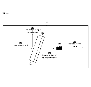
threshold angle shift and with greater than a threshold level of transmission.
100141 Figs. 1A-1C are diagrams of an overview of example implementations
100/100'/100" described herein. As shown in Fig. 1A, example implementation
100 includes a
sensor system 110. Sensor system 110 may be a portion of an optical system,
and may provide
an electrical output corresponding to a sensor determination. Sensor system
110 includes an
optical filter structure 120, which includes an optical filter 130, and an
optical sensor 140. For
example, optical filter structure 120 may include an optical filter 130 that
performs a passband
filtering functionality. In another example, an optical filter 130 may be
aligned to an array of
sensor elements of optical sensor 140.
100151 Although some implementations, described herein, may be described in
terms of an
optical filter in a sensor system, implementations described herein may be
used in another type
of system, may be used external to a sensor system, or the like.
100161 As further shown in Fig. 1A, and by reference number 150, an input
optical signal is
directed toward optical filter structure 120. The input optical signal may
include but is not
limited to light associated with a particular spectral range (e.g., a spectral
range centered at
approximately 1550 nm), such as a spectral range of 1500 nm to 1600 nm, a
spectral range of
1100 nm to 2000 nm, or the like. For example, an optical transmitter may
direct the light toward
optical sensor 140 to permit optical sensor 140 to perform a measurement of
the light. In another
example, the optical transmitter may direct another spectral range of light
for another
functionality, such as a testing functionality, a sensing functionality, a
communications
functionality, or the like.
CA 3010507 2018-07-05
[0017] As further shown in Fig. 1A, and by reference number 160, a first
portion of the
optical signal with a first spectral range is not passed through by optical
filter 130 and optical
filter structure 120. For example, dielectric filter stacks of dielectric thin
film layers, which may
include high index material layers and low index material layers of optical
filter 130, may cause
the first portion of light to be reflected in a first direction, to be
absorbed, or the like. In this
case, the first portion of light may be a threshold portion of light incident
on optical filter 130 not
included in a bandpass of optical filter 130, such as greater than 95% of
light not within a
particular spectral range centered at approximately 1550 nm. As shown by
reference number
170, a second portion of the optical signal is passed through by optical
filter 130 and optical filter
structure 120. For example, optical filter 130 may pass through the second
portion of light with
a second spectral range in a second direction toward optical sensor 140. In
this case, the second
portion of light may be a threshold portion of light incident on optical
filter 130 within a
bandpass of optical filter 130, such as greater than 50% of incident light in
a spectral range
centered at approximately 1550 nm.
[0018] As further shown in Fig. 1A, based on the second portion of the
optical signal being
passed to optical sensor 140, optical sensor 140 may provide an output
electrical signal 180 for
sensor system 110, such as for use in imaging, ambient light sensing,
detecting the presence of
an object, performing a measurement, facilitating communication, or the like.
In some
implementations, another arrangement of optical filter 130 and optical sensor
140 may be
utilized. For example, rather than passing the second portion of the optical
signal collinearly
with the input optical signal, optical filter 130 may direct the second
portion of the optical signal
in another direction toward a differently located optical sensor 140.
6
CA 3010507 2018-07-05
[0019] As shown in Fig. 1B, another example implementation 100' includes a
set of sensor
elements of a sensor element array forming optical sensor 140 and integrated
into a substrate of
optical filter structure 120. In this case, optical filter 130 is disposed
directly onto the substrate.
Input optical signals 150-1 and 150-2 are received at multiple different
angles and first portions
160-1 and 160-2 of input optical signals 150-1 and 150-2 are reflected at
multiple different
angles. In this case, second portions of input optical signals 150-1 and 150-2
are passed through
optical filter 130 to a sensor element array forming optical sensor 140, which
provides an output
electrical signal 180.
[0020] As shown in Fig. 1C, another example implementation 100" includes a
set of sensor
elements of a sensor element array forming optical sensor 140 and separated
from an optical
filter structure 120 (e.g., by free space in a free space optics type of
optical system). In this case,
optical filter 130 is disposed onto optical filter structure 120. Input
optical signals 150-1 and
150-2 are received at multiple different angles at optical filter 130. First
portions 160-1 and 160-
2 of the input optical signals 150-1 and 150-2 are reflected and second
portions 170-1 and 170-2
of the input optical signals 150-1 and 150-2 are passed by optical filter 130
and optical filter
structure 120. Based on receiving second portions 170-1 and 170-2, the sensor
element array
provides an output electrical signal 180.
[0021] As indicated above, Figs. 1A-1C are provided merely as examples.
Other examples
are possible and may differ from what was described with regard to Figs. 1A-
1C.
[0022] Fig. 2 is a diagram of an example optical filter 200. Fig. 2 shows
an example stackup
of an optical filter using hydrogenated germanium as a high index material. As
further shown in
Fig. 2, optical filter 200 includes an optical filter coating portion 210 and
a substrate 220.
7
CA 3010507 2018-07-05
[0023] Optical filter coating portion 210 includes a set of optical filter
layers. For example,
optical filter coating portion 210 includes a first set of layers 230-1
through 230-N (N?: 1) (e.g.,
high refractive index layers (H layers)) and a second set of layers 240-1
through 240-(N+1) (e.g.,
low refractive index layers (L layers)). In some implementations, layers 230
and 240 may be
arranged in a particular order, such as an (H-L),, (11 1?: 1) order, an (H-
L),,-H order, an (L-H)1n
order, an L-(H-L),, order, or the like. For example, as shown, layers 230 and
240 are positioned
in an (H-L),-H order with an H layer disposed at a surface of optical filter
200 and an H layer
contiguous to a surface of substrate 220. In some implementations, one or more
other layers may
be included in optical filter 200, such as one or more protective layers, one
or more layers to
provide one or more other filtering functionalities (e.g., a blocker, an anti-
reflection coating,
etc.), or the like.
[0024] Layers 230 may include a set of hydrogenated germanium layers. In
some
implementations, another material may be utilized for the H layers, such as
another material with
a refractive index greater than the refractive index of the L layers, a
refractive index greater than
2.0, a refractive index greater than 3.0, a refractive index greater than 4.0,
a refractive index
greater than 4.5, a refractive index greater the 4.6, or the like, over a
particular spectral range
(e.g., the spectral range of approximately 1100 nm to approximately 2000 nm,
the spectral range
of approximately 1400 nm to approximately 1600 nm, the wavelength of
approximately 1550
nm, or the like). In another example, layers 230 may be selected to include a
refractive index of
approximately 4.2 at a wavelength of approximately 1550 nm.
[0025] In some implementations, a particular hydrogenated germanium based
material may
be selected for the H layers 230, such as hydrogenated germanium, annealed
hydrogenated
germanium, or the like. In some implementations, layers 230 and/or 240 may be
associated with
8
CA 3010507 2018-07-05
1,
a particular extinction coefficient, such as an extinction coefficient, at
approximately 1550 nm,
of less than approximately 0.1, less than approximately 0.05, less than
approximately 0.01, less
than approximately 0.005, an extinction coefficient of less than approximately
0.001, an
extinction coefficient of less than approximately 0.0008, or the like over a
particular spectral
range (e.g., the spectral range of approximately 800 nm to approximately 2300
nm, the spectral
range of approximately 1100 nm to approximately 2000 nm, the wavelength of
approximately
1550 nm, or the like).
[0026] Layers 240 may include a set of layers silicon dioxide
(SiO2) layers. In some
implementations, another material may be utilized for the L layers. In some
implementations, a
particular material may be selected for L layers 240. For example, layers 240
may include a set
of silicon dioxide (SiO2) layers, a set of aluminum oxide (A1203) layers, a
set of titanium dioxide
(TiO2) layers, a set of niobium pentoxide (Nb2O5) layers, a set of tantalum
pentoxide (Ta205)
layers, a set of magnesium fluoride (MgF2) layers, or the like. In this case,
layers 240 may be
selected to include a refractive index lower than that of the layers 230 over,
for example, a
particular spectral range (e.g., the spectral range of approximately 1100 nm
to approximately
2000 nm, the spectral range of approximately 1400 nm to approximately 1600 nm,
the
wavelength of approximately 1550 nm, or the like). For example, layers 240 may
be selected to
be associated with a refractive index of less than 3 over a particular
spectral range (e.g., the
spectral range of approximately 1100 nm to approximately 2000 nm, the spectral
range of
approximately 1400 nm to approximately 1600 nm, a spectral range of
approximately 800 nm,
the wavelength of approximately 1550 nm, or the like).
[0027] In another example, layers 240 may be selected to be
associated with a refractive
index of less than 2.5 over a particular spectral range (e.g., the spectral
range of approximately
9
CA 3010507 2018-07-05
1100 nm to approximately 2000 nm, the spectral range of approximately 1400 nm
to
approximately 1600 nm, the wavelength of approximately 1550 nm, or the like).
In another
example, layers 240 may be selected to be associated with a refractive index
of less than 2 over a
particular spectral range (e.g., the spectral range of approximately 1100 nm
to approximately
2000 nm, the spectral range of approximately 1400 nm to approximately 1600 nm,
the -
wavelength of approximately 1550 nm, or the like). In another example, layers
240 may be
selected to be associated with a refractive index of less than 1.5 over a
particular spectral range
(e.g., the spectral range of approximately 1100 nm to approximately 2000 nm,
the spectral range
of approximately 1400 nm to approximately 1600 nm, the wavelength of
approximately 1550
nm, or the like). In some implementations, the particular material may be
selected for layers 240
based on a desired width of an out-of-band blocking spectral range, a desired
center-wavelength
shift associated with a change of angle of incidence, or the like.
[0028] In
some implementations, optical filter coating portion 210 may be associated
with a
particular quantity of layers, m. For example, a hydrogenated germanium based
optical filter
may include approximately 20 layers of alternating H layers and L layers. In
another example,
optical filter 200 may be associated with another quantity of layers, such as
a range of 2 layers to
1000 layers, a range of 4 to 50 layers, or the like. In some implementations,
each layer of optical
filter coating portion 210 may be associated with a particular thickness. For
example, layers 230
and 240 may each be associated with a thickness of between approximately 5 nm
and
approximately 2000 nm, resulting in optical filter coating portion 210 being
associated with a
thickness of between approximately 0.2 gm and 100 gm, a thickness of between
approximately
0.5 gm and 20 gm, or the like.
CA 3010507 2018-07-05
[0029] In some implementations, layers 230 and 240 may be associated with
multiple
thicknesses, such as a first thickness for layers 230 and a second thickness
for layers 240, a first
thickness for a first subset of layers 230 and a second thickness for a second
subset of layers 230,
a first thickness for a first subset of layers 240 and a second thickness for
a second subset of
layers 240, or the like. In this case, a layer thickness and/or a quantity of
layers may be selected
based on an intended set of optical characteristics, such as an intended
passband, an intended
transmissivity, or the like. For example, the layer thickness and/or the
quantity of layers may be
selected to permit optical filter 200 to be utilized for a spectral range of
approximately 1100 nm
to approximately 2000 nm, at a center wavelength of approximately 1550 nm, or
the like.
[0030] In some implementations, optical filter coating portion 210 may be
fabricated using a
sputtering procedure. For example, optical filter coating portion 210 may be
fabricated using a
pulsed-magnetron based sputtering procedure to sputter alternating layers 230
and 240 on a glass
substrate. In some implementations, optical filter coating portion 210 may be
associated with a
relatively low center-wavelength shift with change in angle of incidence. For
example, optical
filter coating portion 210 may cause a center-wavelength shift of less than
approximately 20 nm,
less than approximately 15 nm, less than approximately 10 nm, or the like in
magnitude with a
change in incidence angle from 0 degrees to 15 degrees; a center-wavelength
shift of less than
approximately 100 nm, less than approximately 50 nm, less than approximately
30 nm, or the
like with a change in incidence angle from 0 degrees to 30 degrees; a center-
wavelength shift of
less than approximately 200 nm, less than approximately 150 nm, less than
approximately 125
nm, less than approximately 100 nm, or the like with a change in incidence
angle from 0 degrees
to 45 degrees; or the like.
11
CA 3010507 2018-07-05
1,
[0031] In some implementations, optical filter coating portion 210
is attached to a substrate,
such as substrate 220. For example, optical filter coating portion 210 may be
attached to a glass
substrate. In some implementations, optical filter coating portion 210 may be
associated with an
incident medium, such as an air medium or glass medium. In some
implementations, optical
filter 200 may be disposed between a set of prisms.
[0032] In some implementations, an annealing procedure may be
utilized to fabricate optical
filter coating portion 210. For example, after sputter deposition of layers
230 and 240 on a
substrate, optical filter 200 may be annealed to improve one or more optical
characteristics of
optical filter 200, such as reducing an absorption coefficient of optical
filter 200 relative to
another optical filter for which an annealing procedure is not performed.
[0033] As indicated above, Fig. 2 is provided merely as an example.
Other examples are
possible and may differ from what was described with regard to Fig. 2.
[0034] Fig. 3 is diagram of an example 300 of a sputter deposition
system for manufacturing
a hydrogenated germanium based optical filter described herein.
[0035] As shown in Fig. 3, example 300 includes a vacuum chamber
310, a substrate 320, a
cathode 330, a target 331, a cathode power supply 340, an anode 350, a plasma
activation source
(PAS) 360, and a PAS power supply 370. Target 331 may include a germanium
material. PAS
power supply 370 may be utilized to power PAS 360 and may include a radio
frequency (RF)
power supply. Cathode power supply 340 may be utilized to power cathode 330
and may
include a pulsed direct current (DC) power supply.
[0036] With regard to Fig. 3, target 331 is sputtered in the
presence of hydrogen (H2), as well
as an inert gas, such as argon, to deposit a hydrogenated germanium material
as a layer on
substrate 320. The inert gas may be provided into the chamber via anode 350
and/or PAS 360.
12
CA 3010507 2018-07-05
Hydrogen is introduced into the vacuum chamber 310 through PAS 360, which
serves to activate
the hydrogen. Additionally, or alternatively, cathode 330 may cause hydrogen
activation (e.g., in
this case, hydrogen may be introduced from another part of vacuum chamber 310)
or anode 350
may cause hydrogen activation (e.g., in this case, hydrogen may be introduced
into vacuum
chamber 310 by anode 350). In some implementations, the hydrogen may take the
form of
hydrogen gas, a mixture of hydrogen gas and a noble gas (e.g., argon gas), or
the like. PAS 360
may be located within a threshold proximity of cathode 330, allowing plasma
from PAS 360 and
plasma from cathode 330 to overlap. The use of the PAS 360 allows the
hydrogenated
germanium layer to be deposited at a relatively high deposition rate. In some
implementations,
the hydrogenated germanium layer is deposited at a deposition rate of
approximately 0.05 nm/s
to approximately 2.0 nm/s, at a deposition rate of approximately 0.5 nm/s to
approximately 1.2
nm/s, at a deposition rate of approximately 0.8 nm/s, or the like.
[0037] Although the sputtering procedure is described, herein, in
terms of a particular
geometry and a particular implementation, other geometries and other
implementations are
possible. For example, hydrogen may be injected from another direction, from a
gas manifold in
a threshold proximity to cathode 330, or the like. Although, described,
herein, in terms of
different configurations of components, different relative concentrations of
germanium may also
be achieved using different materials, different manufacturing processes, or
the like.
[0038] As indicated above, Fig. 3 is provided merely as an example.
Other examples are
possible and may differ from what was described with regard to Fig. 3.
[0039] Figs. 4A-4D show examples relating to optical filters using
hydrogenated germanium
as a high index material. Figs. 4A-4D show characteristics relating to
hydrogenated germanium
based single layer films.
13
CA 3010507 2018-07-05
1,
[0040] As shown in Fig. 4A, and by chart 400, a filter response showing
transmissivity for a
set of films 410-1 through 410-5 is provided. Each film 410 may be an
approximately 2.5
micrometer single layer film. Film 410-1 is associated with a concentration of
hydrogen
associated with a flow rate of 0 standard cubic centimeters per minute (SCCM).
In other words,
film 410-1 uses non-hydrogenated germanium. Films 410-2, 410-3, 410-4, and 410-
5 are
associated with concentrations of hydrogen associated with flow rates of 20
SCCM, 100 SCCM,
160 SCCM, and 200 SCCM. In other words, films 410-2 through 410-5 use
hydrogenated
germanium with increasing concentrations of hydrogen. In this case, the
hydrogenated
germanium films, such as films 410-2 through 410-5, are associated with
increased
transmissivity relative to non-hydrogenated germanium film 410-1. In this way,
utilizing
hydrogenated germanium in an optical filter can provide improved
transmissivity. For example,
based on a concentration of hydrogen in a hydrogenated germanium film, a
hydrogenated
germanium film may be associated with as a transmissivity greater than 20%,
greater than 40%,
greater than 60%, greater than 80%, greater than 85%, greater than 90%, or the
like for a spectral
range of 1100 nm to 2000 nm, a spectral range of 1400 nm to 1600 nm, a
spectral range with a
wavelength of 1550 nm, or the like.
[0041] As shown in Fig. 4B, and by chart 420, an index of refraction and an
extinction
coefficient for the films 410 are provided. At a wavelength of 1400 nm, non-
hydrogenated
germanium film 410-1 is associated with an extinction coefficient of
approximately 0.1, which is
greater than the extinction coefficients for hydrogenated germanium films 410-
2, 410-3, and
410-5, which are approximately 0.05, approximately 0.005, and approximately
0.002,
respectively. Similarly, at a wavelength of 1400 nm, non-hydrogenated
germanium film 410-1 is
associated with a refractive index of 4.7, which compares with hydrogenated
germanium films
14
CA 3010507 2018-07-05
410-2, 410-3, and 410-5, which are associated with refractive indices of 4.6,
4.4 and 4.3,
respectively. In this case, hydrogenated-germanium films 410-2, 410-3, and 410-
5 are associated
with a reduced extinction coefficient while maintaining a threshold refractive
index (e.g., greater
than 4.0, greater than 4.2, greater than 4.4, greater than 4.5, etc.).
[0042] At a wavelength of 1550 nm, non-hydrogenated germanium film 410-1 is
associated
with an extinction coefficient of approximately 0.07, which is greater than
the extinction
coefficients for hydrogenated germanium films 410-2, 410-3, and 410-5, which
are
approximately 0.03, approximately 0.003, and approximately 0.001,
respectively. Similarly, at a
wavelength of 1550 nm, non-hydrogenated germanium film 410-1 is associated
with a refractive
index of 4.6, which compares with hydrogenated germanium films 410-2, 410-3,
and 410-5,
which are associated with refractive indices of 4.4, 4.3 and 4.2,
respectively. In this case,
hydrogenated-germanium films 410-2, 410-3, and 410-5 are associated with a
reduced extinction
coefficient while maintaining a threshold refractive index (e.g., greater than
4.0, greater than 4.2,
greater than 4.4, etc.).
[0043] At a wavelength of 2000 nm, non-hydrogenated germanium film 410-1 is
associated
with an extinction coefficient of approximately 0.05, which is greater than
the extinction
coefficients for hydrogenated germanium films 410-2, 410-3, and 410-5, which
are
approximately 0.005, approximately 0.0005, and approximately 0.000001,
respectively.
Similarly, at a wavelength of 1550 nm, non-hydrogenated germanium film 410-1
is associated
with a refractive index of 4.5, which compares with hydrogenated germanium
films 410-2, 410-
3, and 410-5, which are associated with refractive indices of 4.4, 4.2 and
4.1, respectively. In
this case, hydrogenated-germanium films 410-2, 410-3, and 410-5 are associated
with a reduced
CA 3010507 2018-07-05
extinction coefficient while maintaining a threshold refractive index (e.g.,
greater than 3.5,
greater than 3.75, greater than 4.0).
[0044] As shown in Fig. 4C, and by chart 430, an index of refraction for
hydrogenated
germanium film 410-5 and a hydrogenated silicon film 410-6 is provided. In
this case, the index
of refraction for hydrogenated germanium film 410-5 is each greater than an
index of refraction
for hydrogenated silicon film 410-6.
[0045] As shown in Fig. 4D, and by chart 440, an index of refraction and an
extinction
coefficient are provided for hydrogenated germanium film 410-5 and an annealed
hydrogenated
germanium film 410-5'. In this case, applying an annealing procedure, for
example, at
approximately 300 degrees Celsius for 60 minutes results in forming annealed
hydrogenated
germanium film 410-5', results in an increased index of refraction (e.g.,
increased to
approximately 4.3) and a reduced extinction coefficient (e.g., reduced to
approximately 0.0006)
at a spectral range with a center wavelength of approximately 1550 nm relative
to hydrogenated
germanium film 410-5, thereby reducing angle shift and improving
transmissivity.
[0046] As indicated above, Figs. 4A-4D are provided merely as examples.
Other examples
are possible and may differ from what was described with regard to Figs. 4A-
4D.
[0047] Figs. 5A-5C are diagrams of characteristics relating to an optical
filter. Figs. 5A-5C
show characteristics relating to bandpass filters.
[0048] As shown in Fig. 5A, and by chart 500, a filter response is provided
for a
hydrogenated germanium optical filter 510. Optical filter 510 may include
alternating layers of
hydrogenated germanium and silicon dioxide. In some implementations, optical
filter 510 may
be associated with a thickness of approximately 5.6 gm, and may be associated
with a bandpass
centered at approximately 1550 nm for an angle of incidence of 0 degrees.
Moreover, optical
16
CA 3010507 2018-07-05
filter 510 is associated with a transmissivity of greater than a threshold
amount (e.g., greater than
approximately 90%) for angles of incidence from 0 degrees to 40 degrees.
[0049] As shown in Fig. 5B, and by chart 520, a filter response is provided
for a
hydrogenated silicon based optical filter 530. Optical filter 530 may include
alternating layers of
hydrogenated silicon and silicon dioxide. In some implementations, optical
filter 530 may be
associated with a thickness of approximately 5.9 micrometers (vim) and may be
associated with a
bandpass centered at approximately 1550 nm for an angle of incidence of 0
degrees.
[0050] As shown in Fig. 5C, and by chart 540, relative to optical filter
510 (Si:Ge), optical
filter 530 (Si:H) is associated with a reduced angle shift for changes of
angles of incidence from
0 degrees to approximately 40 degrees. For example, optical filter 510 is
associated with a
change in center wavelength of, for example, less than approximately 5 nm at
an angle of
incidence of approximately 0-10 degrees, less than approximately 4 nm at an
angle of incidence
of approximately 0-10 degrees, less than approximately 3 nm at an angle of
incidence of
approximately 0-10 degrees, less than approximately 2 nm at an angle of
incidence of
approximately 0-10 degrees, or the like. Similarly, optical filter 510 is
associated with a change
in center wavelength of, for example, less than approximately 15 nm at an
angle of incidence of
10-20 degrees, less than approximately 10 nm at an angle of incidence of 10-20
degrees, less
than approximately 9 nm at an angle of incidence of 10-20 degrees, less than
approximately 8
nm at an angle of incidence of 10-20 degrees, or the like.
[0051] Similarly, optical filter 510 is associated with a change in center
wavelength of, for
example, less than approximately 8 nm at an angle of incidence of 20 degrees,
less than
approximately 9 nm at an angle of incidence of 20 degrees, less than
approximately 30 nm at an
angle of incidence of 20-30 degrees, less than approximately 20 nm at an angle
of incidence of
17
CA 3010507 2018-07-05
1,
20-30 degrees, less than approximately 15 nm at an angle of incidence of 20-30
degrees, less
than approximately 10 nm at an angle of incidence of 20-30 degrees, or the
like. Similarly,
optical filter 510 is associated with a change in center wavelength of, for
example, less than
approximately 40 nm at an angle of incidence of approximately 30-40 degrees,
less than
approximately 35 nm at an angle of incidence of approximately 30-40 degrees,
less than
approximately 30 nm at an angle of incidence of approximately 30-40 degrees,
less than
approximately 25 nm at an angle of incidence of approximately 30-40 degrees,
less than
approximately 20 nm at an angle of incidence of approximately 30-40 degrees,
or the like.
[0052] As indicated above, Figs. 5A-5C are provided merely as
examples. Other examples
are possible and may differ from what was described with regard to Figs. 5A-
5C.
[0053] In this way, a hydrogenated germanium optical filter, such
as an optical filter with
hydrogenated germanium as a high index layer and another material as a low
index layer, may
provide improved angel shift, improved transmissivity, and reduced physical
thickness relative to
other materials for an optical filter associated with a spectral range with a
center wavelength at
approximately 1550 nm.
[0054] The foregoing disclosure provides illustration and
description, but is not intended to
be exhaustive or to limit the implementations to the precise form disclosed.
Modifications and
variations are possible in light of the above disclosure or may be acquired
from practice of the
implementations.
[0055] Some implementations are described herein in connection with
thresholds. As used
herein, satisfying a threshold may refer to a value being greater than the
threshold, more than the
threshold, higher than the threshold, greater than or equal to the threshold,
less than the
18
CA 3010507 2018-07-05
threshold, fewer than the threshold, lower than the threshold, less than or
equal to the threshold,
equal to the threshold, etc.
[0056] Even though particular combinations of features are recited in the
claims and/or
disclosed in the specification, these combinations are not intended to limit
the disclosure of
possible implementations. In fact, many of these features may be combined in
ways not
specifically recited in the claims and/or disclosed in the specification.
Although each dependent
claim listed below may directly depend on only one claim, the disclosure of
possible
implementations includes each dependent claim in combination with every other
claim in the
claim set.
[0057] No element, act, or instruction used herein should be construed as
critical or essential
unless explicitly described as such. Also, as used herein, the articles "a"
and "an" are intended to
include one or more items, and may be used interchangeably with "one or more."
Furthermore,
as used herein, the term "set" is intended to include one or more items (e.g.,
related items,
unrelated items, a combination of related items, and unrelated items, etc.),
and may be used
interchangeably with "one or more." Where only one item is intended, the term
"one" or similar
language is used. Also, as used herein, the terms "has," "have," "having," or
the like are
intended to be open-ended terms. Further, the phrase "based on" is intended to
mean "based, at
least in part, on" unless explicitly stated otherwise.
19
CA 3010507 2018-07-05